STM8L151x4, STM8L151x6,
STM8L152x4, STM8L152x6
8-bit ultra-low-power MCU, up to 32 KB Flash, 1 KB Data EEPROM,
RTC, LCD, timers, USART, I2C, SPI, ADC, DAC, comparators
Datasheet - production data
Features
• Operating conditions
– Operating power supply range 1.8 V to
3.6 V (down to 1.65 V at power down)
– Temp. range: - 40 °C to 85, 105 or 125 °C
• Low power features
– 5 low power modes: Wait, Low power run
(5.1 µA), Low power wait (3 µA), Active-halt
with full RTC (1.3 µA), Halt (350 nA)
– Consumption: 195 µA/MHz + 440 µA
– Ultra-low leakage per I/0: 50 nA
– Fast wakeup from Halt: 4.7 µs
• Advanced STM8 core
– Harvard architecture and 3-stage pipeline
– Max freq. 16 MHz, 16 CISC MIPS peak
– Up to 40 external interrupt sources
• Reset and supply management
– Low power, ultra-safe BOR reset with 5
selectable thresholds
– Ultra-low-power POR/PDR
– Programmable voltage detector (PVD)
• Clock management
– 1 to 16 MHz crystal oscillator
– 32 kHz crystal oscillator
– Internal 16 MHz factory-trimmed RC
– Internal 38 kHz low consumption RC
– Clock security system
• Low power RTC
– BCD calendar with alarm interrupt
– Auto-wakeup from Halt w/ periodic interrupt
• LCD: up to 4x28 segments w/ step-up
converter
• Memories
– Up to 32 KB of Flash program memory and
1 Kbyte of data EEPROM with ECC, RWW
– Flexible write and read protection modes
– Up to 2 Kbyte of RAM
• DMA
– 4 channels; supported peripherals: ADC,
DAC, SPI, I2C, USART, timers
– 1 channel for memory-to-memory
April 2017
This is information on a product in full production.
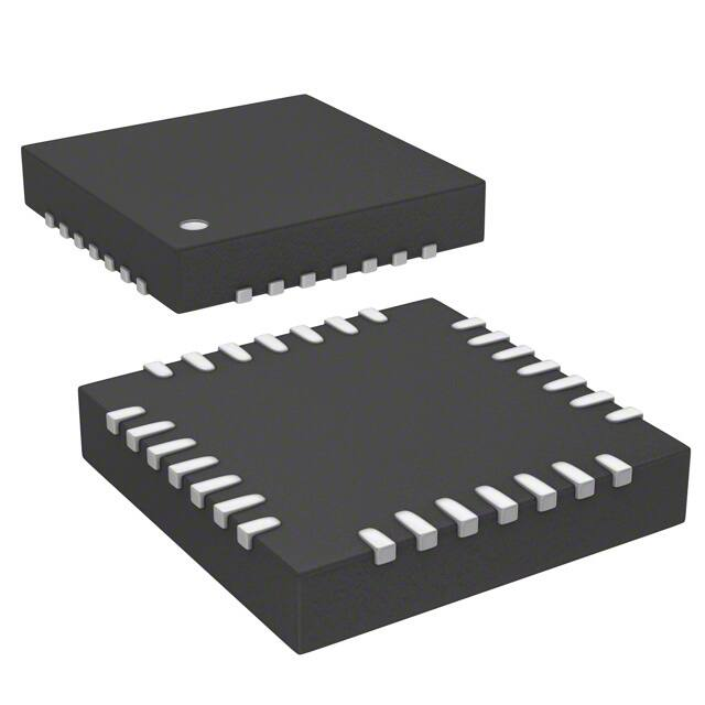
UFQFPN48
7x7 mm
LQFP48
7x7 mm
UFQFPN32 (5x5 mm)
LQFP32
7x7 mm
UFQFPN28 (4x4 mm)
#30
WLCSP28
• 12-bit DAC with output buffer
• 12-bit ADC up to 1 Msps/25 channels
– T. sensor and internal reference voltage
• 2 ultra-low-power comparators
– 1 with fixed threshold and 1 rail to rail
– Wakeup capability
• Timers
– Two 16-bit timers with 2 channels (used as
IC, OC, PWM), quadrature encoder
– One 16-bit advanced control timer with 3
channels, supporting motor control
– One 8-bit timer with 7-bit prescaler
– 2 watchdogs: 1 Window, 1 Independent
– Beeper timer with 1, 2 or 4 kHz frequencies
• Communication interfaces
– Synchronous serial interface (SPI)
– Fast I2C 400 kHz SMBus and PMBus
– USART (ISO 7816 interface and IrDA)
• Up to 41 I/Os, all mappable on interrupt vectors
• Up to 16 capacitive sensing channels
supporting touchkey, proximity, linear touch
and rotary touch sensors
• Development support
– Fast on-chip programming and non
intrusive debugging with SWIM
– Bootloader using USART
• 96-bit unique ID
Table 1. Device summary
Reference
Part number
STM8L151xx
(without LCD)
STM8L151C4, STM8L151C6, STM8L151K4,
STM8L151K6, STM8L151G4, STM8L151G6
STM8L152xx
(with LCD)
STM8L152C4, STM8L152C6, STM8L152K4,
STM8L152K6
DocID15962 Rev 15
1/142
www.st.com
�Contents
STM8L151x4/6, STM8L152x4/6
Contents
1
Introduction . . . . . . . . . . . . . . . . . . . . . . . . . . . . . . . . . . . . . . . . . . . . . . . . 9
2
Description . . . . . . . . . . . . . . . . . . . . . . . . . . . . . . . . . . . . . . . . . . . . . . . . 11
3
2.1
Device overview . . . . . . . . . . . . . . . . . . . . . . . . . . . . . . . . . . . . . . . . . . . . 12
2.2
Ultra-low-power continuum . . . . . . . . . . . . . . . . . . . . . . . . . . . . . . . . . . . . 13
Functional overview . . . . . . . . . . . . . . . . . . . . . . . . . . . . . . . . . . . . . . . . 14
3.1
Low-power modes . . . . . . . . . . . . . . . . . . . . . . . . . . . . . . . . . . . . . . . . . . 15
3.2
Central processing unit STM8 . . . . . . . . . . . . . . . . . . . . . . . . . . . . . . . . . 16
3.3
Advanced STM8 Core . . . . . . . . . . . . . . . . . . . . . . . . . . . . . . . . . . . . . . 16
3.2.2
Interrupt controller . . . . . . . . . . . . . . . . . . . . . . . . . . . . . . . . . . . . . . . . . 16
Reset and supply management . . . . . . . . . . . . . . . . . . . . . . . . . . . . . . . . 17
3.3.1
Power supply scheme . . . . . . . . . . . . . . . . . . . . . . . . . . . . . . . . . . . . . . 17
3.3.2
Power supply supervisor . . . . . . . . . . . . . . . . . . . . . . . . . . . . . . . . . . . . 17
3.3.3
Voltage regulator . . . . . . . . . . . . . . . . . . . . . . . . . . . . . . . . . . . . . . . . . . 17
3.4
Clock management . . . . . . . . . . . . . . . . . . . . . . . . . . . . . . . . . . . . . . . . . 18
3.5
Low power real-time clock . . . . . . . . . . . . . . . . . . . . . . . . . . . . . . . . . . . . 19
3.6
LCD (Liquid crystal display) . . . . . . . . . . . . . . . . . . . . . . . . . . . . . . . . . . . 20
3.7
Memories . . . . . . . . . . . . . . . . . . . . . . . . . . . . . . . . . . . . . . . . . . . . . . . . . 20
3.8
DMA . . . . . . . . . . . . . . . . . . . . . . . . . . . . . . . . . . . . . . . . . . . . . . . . . . . . . 20
3.9
Analog-to-digital converter . . . . . . . . . . . . . . . . . . . . . . . . . . . . . . . . . . . . 20
3.10
Digital-to-analog converter (DAC) . . . . . . . . . . . . . . . . . . . . . . . . . . . . . . 21
3.11
Ultra-low-power comparators . . . . . . . . . . . . . . . . . . . . . . . . . . . . . . . . . . 21
3.12
System configuration controller and routing interface . . . . . . . . . . . . . . . 21
3.13
Touch sensing . . . . . . . . . . . . . . . . . . . . . . . . . . . . . . . . . . . . . . . . . . . . . 21
3.14
Timers . . . . . . . . . . . . . . . . . . . . . . . . . . . . . . . . . . . . . . . . . . . . . . . . . . . 22
3.15
2/142
3.2.1
3.14.1
TIM1 - 16-bit advanced control timer . . . . . . . . . . . . . . . . . . . . . . . . . . . 22
3.14.2
16-bit general purpose timers . . . . . . . . . . . . . . . . . . . . . . . . . . . . . . . . 23
3.14.3
8-bit basic timer . . . . . . . . . . . . . . . . . . . . . . . . . . . . . . . . . . . . . . . . . . . 23
Watchdog timers . . . . . . . . . . . . . . . . . . . . . . . . . . . . . . . . . . . . . . . . . . . 23
3.15.1
Window watchdog timer . . . . . . . . . . . . . . . . . . . . . . . . . . . . . . . . . . . . . 23
3.15.2
Independent watchdog timer . . . . . . . . . . . . . . . . . . . . . . . . . . . . . . . . . 23
DocID15962 Rev 15
�STM8L151x4/6, STM8L152x4/6
4
3.16
Beeper . . . . . . . . . . . . . . . . . . . . . . . . . . . . . . . . . . . . . . . . . . . . . . . . . . . 23
3.17
Communication interfaces . . . . . . . . . . . . . . . . . . . . . . . . . . . . . . . . . . . . 24
3.17.1
SPI . . . . . . . . . . . . . . . . . . . . . . . . . . . . . . . . . . . . . . . . . . . . . . . . . . . . . 24
3.17.2
I²C . . . . . . . . . . . . . . . . . . . . . . . . . . . . . . . . . . . . . . . . . . . . . . . . . . . . . 24
3.17.3
USART . . . . . . . . . . . . . . . . . . . . . . . . . . . . . . . . . . . . . . . . . . . . . . . . . . 24
3.18
Infrared (IR) interface . . . . . . . . . . . . . . . . . . . . . . . . . . . . . . . . . . . . . . . . 24
3.19
Development support . . . . . . . . . . . . . . . . . . . . . . . . . . . . . . . . . . . . . . . . 25
Pinout and pin description . . . . . . . . . . . . . . . . . . . . . . . . . . . . . . . . . . . 26
4.1
5
Contents
System configuration options . . . . . . . . . . . . . . . . . . . . . . . . . . . . . . . . . . 37
Memory and register map . . . . . . . . . . . . . . . . . . . . . . . . . . . . . . . . . . . . 38
5.1
Memory mapping . . . . . . . . . . . . . . . . . . . . . . . . . . . . . . . . . . . . . . . . . . . 38
5.2
Register map . . . . . . . . . . . . . . . . . . . . . . . . . . . . . . . . . . . . . . . . . . . . . . 39
6
Interrupt vector mapping . . . . . . . . . . . . . . . . . . . . . . . . . . . . . . . . . . . . 57
7
Option bytes . . . . . . . . . . . . . . . . . . . . . . . . . . . . . . . . . . . . . . . . . . . . . . 59
8
Unique ID . . . . . . . . . . . . . . . . . . . . . . . . . . . . . . . . . . . . . . . . . . . . . . . . . 62
9
Electrical parameters . . . . . . . . . . . . . . . . . . . . . . . . . . . . . . . . . . . . . . . 63
9.1
Parameter conditions . . . . . . . . . . . . . . . . . . . . . . . . . . . . . . . . . . . . . . . . 63
9.1.1
Minimum and maximum values . . . . . . . . . . . . . . . . . . . . . . . . . . . . . . . 63
9.1.2
Typical values . . . . . . . . . . . . . . . . . . . . . . . . . . . . . . . . . . . . . . . . . . . . 63
9.1.3
Typical curves . . . . . . . . . . . . . . . . . . . . . . . . . . . . . . . . . . . . . . . . . . . . 63
9.1.4
Loading capacitor . . . . . . . . . . . . . . . . . . . . . . . . . . . . . . . . . . . . . . . . . 63
9.1.5
Pin input voltage . . . . . . . . . . . . . . . . . . . . . . . . . . . . . . . . . . . . . . . . . . 64
9.2
Absolute maximum ratings . . . . . . . . . . . . . . . . . . . . . . . . . . . . . . . . . . . . 64
9.3
Operating conditions . . . . . . . . . . . . . . . . . . . . . . . . . . . . . . . . . . . . . . . . 66
9.3.1
General operating conditions . . . . . . . . . . . . . . . . . . . . . . . . . . . . . . . . . 66
9.3.2
Embedded reset and power control block characteristics . . . . . . . . . . . 67
9.3.3
Supply current characteristics . . . . . . . . . . . . . . . . . . . . . . . . . . . . . . . . 68
9.3.4
Clock and timing characteristics . . . . . . . . . . . . . . . . . . . . . . . . . . . . . . 82
9.3.5
Memory characteristics . . . . . . . . . . . . . . . . . . . . . . . . . . . . . . . . . . . . . 88
9.3.6
I/O current injection characteristics . . . . . . . . . . . . . . . . . . . . . . . . . . . . 89
9.3.7
I/O port pin characteristics . . . . . . . . . . . . . . . . . . . . . . . . . . . . . . . . . . . 89
DocID15962 Rev 15
3/142
4
�Contents
10
STM8L151x4/6, STM8L152x4/6
9.3.8
Communication interfaces . . . . . . . . . . . . . . . . . . . . . . . . . . . . . . . . . . . 97
9.3.9
LCD controller (STM8L152xx only) . . . . . . . . . . . . . . . . . . . . . . . . . . . 102
9.3.10
Embedded reference voltage . . . . . . . . . . . . . . . . . . . . . . . . . . . . . . . . 103
9.3.11
Temperature sensor . . . . . . . . . . . . . . . . . . . . . . . . . . . . . . . . . . . . . . . 104
9.3.12
Comparator characteristics . . . . . . . . . . . . . . . . . . . . . . . . . . . . . . . . . 104
9.3.13
12-bit DAC characteristics . . . . . . . . . . . . . . . . . . . . . . . . . . . . . . . . . . 106
9.3.14
12-bit ADC1 characteristics . . . . . . . . . . . . . . . . . . . . . . . . . . . . . . . . . 108
9.3.15
EMC characteristics . . . . . . . . . . . . . . . . . . . . . . . . . . . . . . . . . . . . . . . 114
Package information . . . . . . . . . . . . . . . . . . . . . . . . . . . . . . . . . . . . . . . 116
10.1
ECOPACK . . . . . . . . . . . . . . . . . . . . . . . . . . . . . . . . . . . . . . . . . . . . . . . .116
10.2
LQFP48 package information . . . . . . . . . . . . . . . . . . . . . . . . . . . . . . . . . .116
10.3
UFQFPN48 package information . . . . . . . . . . . . . . . . . . . . . . . . . . . . . . 120
10.4
LQFP32 package information . . . . . . . . . . . . . . . . . . . . . . . . . . . . . . . . . 123
10.5
UFQFPN32 package information . . . . . . . . . . . . . . . . . . . . . . . . . . . . . . 126
10.6
UFQFPN28 package information . . . . . . . . . . . . . . . . . . . . . . . . . . . . . . 129
10.7
WLCSP28 package information . . . . . . . . . . . . . . . . . . . . . . . . . . . . . . . 132
10.8
Thermal characteristics . . . . . . . . . . . . . . . . . . . . . . . . . . . . . . . . . . . . . 135
11
Part numbering . . . . . . . . . . . . . . . . . . . . . . . . . . . . . . . . . . . . . . . . . . . 136
12
Revision history . . . . . . . . . . . . . . . . . . . . . . . . . . . . . . . . . . . . . . . . . . 137
4/142
DocID15962 Rev 15
�STM8L151x4/6, STM8L152x4/6
List of tables
List of tables
Table 1.
Table 2.
Table 3.
Table 4.
Table 5.
Table 6.
Table 7.
Table 8.
Table 9.
Table 10.
Table 11.
Table 12.
Table 13.
Table 14.
Table 15.
Table 16.
Table 17.
Table 18.
Table 19.
Table 20.
Table 21.
Table 22.
Table 23.
Table 24.
Table 25.
Table 26.
Table 27.
Table 28.
Table 29.
Table 30.
Table 31.
Table 32.
Table 33.
Table 34.
Table 35.
Table 36.
Table 37.
Table 38.
Table 39.
Table 40.
Table 41.
Table 42.
Table 43.
Table 44.
Table 45.
Table 46.
Device summary . . . . . . . . . . . . . . . . . . . . . . . . . . . . . . . . . . . . . . . . . . . . . . . . . . . . . . . . . . 1
Medium-density STM8L151x4/6 and STM8L152x4/6 low-power device features and
peripheral counts . . . . . . . . . . . . . . . . . . . . . . . . . . . . . . . . . . . . . . . . . . . . . . . . . . . . . . . . 12
Timer feature comparison . . . . . . . . . . . . . . . . . . . . . . . . . . . . . . . . . . . . . . . . . . . . . . . . . . 22
Legend/abbreviation for table 5 . . . . . . . . . . . . . . . . . . . . . . . . . . . . . . . . . . . . . . . . . . . . . 29
Medium-density STM8L151x4/6, STM8L152x4/6 pin description. . . . . . . . . . . . . . . . . . . . 29
Flash and RAM boundary addresses . . . . . . . . . . . . . . . . . . . . . . . . . . . . . . . . . . . . . . . . . 39
Factory conversion registers. . . . . . . . . . . . . . . . . . . . . . . . . . . . . . . . . . . . . . . . . . . . . . . . 39
I/O port hardware register map . . . . . . . . . . . . . . . . . . . . . . . . . . . . . . . . . . . . . . . . . . . . . . 39
General hardware register map . . . . . . . . . . . . . . . . . . . . . . . . . . . . . . . . . . . . . . . . . . . . . 40
CPU/SWIM/debug module/interrupt controller registers . . . . . . . . . . . . . . . . . . . . . . . . . . . 55
Interrupt mapping . . . . . . . . . . . . . . . . . . . . . . . . . . . . . . . . . . . . . . . . . . . . . . . . . . . . . . . . 57
Option byte addresses . . . . . . . . . . . . . . . . . . . . . . . . . . . . . . . . . . . . . . . . . . . . . . . . . . . . 59
Option byte description . . . . . . . . . . . . . . . . . . . . . . . . . . . . . . . . . . . . . . . . . . . . . . . . . . . . 60
Unique ID registers (96 bits) . . . . . . . . . . . . . . . . . . . . . . . . . . . . . . . . . . . . . . . . . . . . . . . . 62
Voltage characteristics . . . . . . . . . . . . . . . . . . . . . . . . . . . . . . . . . . . . . . . . . . . . . . . . . . . . 64
Current characteristics . . . . . . . . . . . . . . . . . . . . . . . . . . . . . . . . . . . . . . . . . . . . . . . . . . . . 65
Thermal characteristics. . . . . . . . . . . . . . . . . . . . . . . . . . . . . . . . . . . . . . . . . . . . . . . . . . . . 65
General operating conditions . . . . . . . . . . . . . . . . . . . . . . . . . . . . . . . . . . . . . . . . . . . . . . . 66
Embedded reset and power control block characteristics. . . . . . . . . . . . . . . . . . . . . . . . . . 67
Total current consumption in Run mode . . . . . . . . . . . . . . . . . . . . . . . . . . . . . . . . . . . . . . . 69
Total current consumption in Wait mode . . . . . . . . . . . . . . . . . . . . . . . . . . . . . . . . . . . . . . 71
Total current consumption and timing in Low power run mode
at VDD = 1.65 V to 3.6 V . . . . . . . . . . . . . . . . . . . . . . . . . . . . . . . . . . . . . . . . . . . . . . . . . . 74
Total current consumption in Low power wait mode at VDD = 1.65 V to 3.6 V . . . . . . . . . 76
Total current consumption and timing in Active-halt mode at VDD = 1.65 V to 3.6 V. . . . . 78
Typical current consumption in Active-halt mode, RTC clocked by LSE external crystal . . 80
Total current consumption and timing in Halt mode at VDD = 1.65 to 3.6 V . . . . . . . . . . . 80
Peripheral current consumption . . . . . . . . . . . . . . . . . . . . . . . . . . . . . . . . . . . . . . . . . . . . . 81
Current consumption under external reset . . . . . . . . . . . . . . . . . . . . . . . . . . . . . . . . . . . . . 82
HSE external clock characteristics . . . . . . . . . . . . . . . . . . . . . . . . . . . . . . . . . . . . . . . . . . . 82
LSE external clock characteristics . . . . . . . . . . . . . . . . . . . . . . . . . . . . . . . . . . . . . . . . . . . 82
HSE oscillator characteristics . . . . . . . . . . . . . . . . . . . . . . . . . . . . . . . . . . . . . . . . . . . . . . . 83
LSE oscillator characteristics . . . . . . . . . . . . . . . . . . . . . . . . . . . . . . . . . . . . . . . . . . . . . . . 84
HSI oscillator characteristics. . . . . . . . . . . . . . . . . . . . . . . . . . . . . . . . . . . . . . . . . . . . . . . . 85
LSI oscillator characteristics . . . . . . . . . . . . . . . . . . . . . . . . . . . . . . . . . . . . . . . . . . . . . . . . 86
RAM and hardware registers . . . . . . . . . . . . . . . . . . . . . . . . . . . . . . . . . . . . . . . . . . . . . . . 88
Flash program and data EEPROM memory . . . . . . . . . . . . . . . . . . . . . . . . . . . . . . . . . . . . 88
I/O current injection susceptibility . . . . . . . . . . . . . . . . . . . . . . . . . . . . . . . . . . . . . . . . . . . . 89
I/O static characteristics . . . . . . . . . . . . . . . . . . . . . . . . . . . . . . . . . . . . . . . . . . . . . . . . . . . 90
Output driving current (high sink ports). . . . . . . . . . . . . . . . . . . . . . . . . . . . . . . . . . . . . . . . 93
Output driving current (true open drain ports). . . . . . . . . . . . . . . . . . . . . . . . . . . . . . . . . . . 93
Output driving current (PA0 with high sink LED driver capability). . . . . . . . . . . . . . . . . . . . 93
NRST pin characteristics . . . . . . . . . . . . . . . . . . . . . . . . . . . . . . . . . . . . . . . . . . . . . . . . . . 95
SPI1 characteristics . . . . . . . . . . . . . . . . . . . . . . . . . . . . . . . . . . . . . . . . . . . . . . . . . . . . . . 97
I2C characteristics . . . . . . . . . . . . . . . . . . . . . . . . . . . . . . . . . . . . . . . . . . . . . . . . . . . . . . 100
LCD characteristics. . . . . . . . . . . . . . . . . . . . . . . . . . . . . . . . . . . . . . . . . . . . . . . . . . . . . . 102
Reference voltage characteristics. . . . . . . . . . . . . . . . . . . . . . . . . . . . . . . . . . . . . . . . . . . 103
DocID15962 Rev 15
5/142
6
�List of tables
Table 47.
Table 48.
Table 49.
Table 50.
Table 51.
Table 52.
Table 53.
Table 54.
Table 55.
Table 56.
Table 57.
Table 58.
Table 59.
Table 60.
Table 61.
Table 62.
Table 63.
Table 64.
Table 65.
Table 66.
Table 67.
Table 68.
Table 69.
6/142
STM8L151x4/6, STM8L152x4/6
TS characteristics . . . . . . . . . . . . . . . . . . . . . . . . . . . . . . . . . . . . . . . . . . . . . . . . . . . . . . . 104
Comparator 1 characteristics . . . . . . . . . . . . . . . . . . . . . . . . . . . . . . . . . . . . . . . . . . . . . . 104
Comparator 2 characteristics . . . . . . . . . . . . . . . . . . . . . . . . . . . . . . . . . . . . . . . . . . . . . . 105
DAC characteristics . . . . . . . . . . . . . . . . . . . . . . . . . . . . . . . . . . . . . . . . . . . . . . . . . . . . . 106
DAC accuracy . . . . . . . . . . . . . . . . . . . . . . . . . . . . . . . . . . . . . . . . . . . . . . . . . . . . . . . . . . 107
DAC output on PB4-PB5-PB6 . . . . . . . . . . . . . . . . . . . . . . . . . . . . . . . . . . . . . . . . . . . . . 107
ADC1 characteristics . . . . . . . . . . . . . . . . . . . . . . . . . . . . . . . . . . . . . . . . . . . . . . . . . . . . 108
ADC1 accuracy with VDDA = 3.3 V to 2.5 V. . . . . . . . . . . . . . . . . . . . . . . . . . . . . . . . . . . 110
ADC1 accuracy with VDDA = 2.4 V to 3.6 V. . . . . . . . . . . . . . . . . . . . . . . . . . . . . . . . . . . 110
ADC1 accuracy with VDDA = VREF+ = 1.8 V to 2.4 V. . . . . . . . . . . . . . . . . . . . . . . . . . . 110
RAIN max for fADC = 16 MHz . . . . . . . . . . . . . . . . . . . . . . . . . . . . . . . . . . . . . . . . . . . . . . . 112
EMS data . . . . . . . . . . . . . . . . . . . . . . . . . . . . . . . . . . . . . . . . . . . . . . . . . . . . . . . . . . . . . 114
EMI data . . . . . . . . . . . . . . . . . . . . . . . . . . . . . . . . . . . . . . . . . . . . . . . . . . . . . . . . . . . . . 115
ESD absolute maximum ratings . . . . . . . . . . . . . . . . . . . . . . . . . . . . . . . . . . . . . . . . . . . . 115
Electrical sensitivities . . . . . . . . . . . . . . . . . . . . . . . . . . . . . . . . . . . . . . . . . . . . . . . . . . . . 115
LQFP48 - 48-pin, 7 x 7 mm low-profile quad flat package
mechanical data . . . . . . . . . . . . . . . . . . . . . . . . . . . . . . . . . . . . . . . . . . . . . . . . . . . . . . . . 117
UFQFPN48 - 48-lead, 7 x 7 mm, 0.5 mm pitch, ultra thin fine pitch quad flat
package mechanical data . . . . . . . . . . . . . . . . . . . . . . . . . . . . . . . . . . . . . . . . . . . . . . . . . 121
LQFP32 - 32-pin, 7 x 7 mm low-profile quad flat package
mechanical data . . . . . . . . . . . . . . . . . . . . . . . . . . . . . . . . . . . . . . . . . . . . . . . . . . . . . . . . 124
UFQFPN32 - 32-pin, 5 x 5 mm, 0.5 mm pitch ultra thin fine pitch quad flat
package mechanical data . . . . . . . . . . . . . . . . . . . . . . . . . . . . . . . . . . . . . . . . . . . . . . . . . 127
UFQFPN28 - 28-lead, 4 x 4 mm, 0.5 mm pitch, ultra thin fine pitch quad flat
package mechanical data . . . . . . . . . . . . . . . . . . . . . . . . . . . . . . . . . . . . . . . . . . . . . . . . . 129
WLCSP28 - 28-pin, 1.703 x 2.841 mm, 0.4 mm pitch wafer level chip scale
package mechanical data . . . . . . . . . . . . . . . . . . . . . . . . . . . . . . . . . . . . . . . . . . . . . . . . . 133
Thermal characteristics. . . . . . . . . . . . . . . . . . . . . . . . . . . . . . . . . . . . . . . . . . . . . . . . . . . 135
Document revision history . . . . . . . . . . . . . . . . . . . . . . . . . . . . . . . . . . . . . . . . . . . . . . . . 137
DocID15962 Rev 15
�STM8L151x4/6, STM8L152x4/6
List of figures
List of figures
Figure 1.
Figure 2.
Figure 3.
Figure 4.
Figure 5.
Figure 6.
Figure 7.
Figure 8.
Figure 9.
Figure 10.
Figure 11.
Figure 12.
Figure 13.
Figure 14.
Figure 15.
Figure 16.
Figure 17.
Figure 18.
Figure 19.
Figure 20.
Figure 21.
Figure 22.
Figure 23.
Figure 24.
Figure 25.
Figure 26.
Figure 27.
Figure 28.
Figure 29.
Figure 30.
Figure 31.
Figure 32.
Figure 33.
Figure 34.
Figure 35.
Figure 36.
Figure 37.
Figure 38.
Figure 39.
Figure 40.
Figure 41.
Figure 42.
Figure 43.
Figure 44.
Figure 45.
Figure 46.
Medium-density STM8L151x4/6 and STM8L152x4/6 device block diagram . . . . . . . . . . . 14
Medium-density STM8L151x4/6 and STM8L152x4/6 clock tree diagram . . . . . . . . . . . . . 19
STM8L151C4, STM8L151C6 48-pin pinout (without LCD). . . . . . . . . . . . . . . . . . . . . . . . . 26
STM8L151K4, STM8L151K6 32-pin package pinout (without LCD). . . . . . . . . . . . . . . . . . 26
STM8L151Gx UFQFPN28 package pinout . . . . . . . . . . . . . . . . . . . . . . . . . . . . . . . . . . . . 26
STM8L151G4, STM8L151G6 WLCSP28 package pinout . . . . . . . . . . . . . . . . . . . . . . . . . 27
STM8L152C4, STM8L152C6 48-pin pinout (with LCD) . . . . . . . . . . . . . . . . . . . . . . . . . . . 27
STM8L152K4, STM8L152K6 32-pin package pinout (with LCD) . . . . . . . . . . . . . . . . . . . . 28
Memory map . . . . . . . . . . . . . . . . . . . . . . . . . . . . . . . . . . . . . . . . . . . . . . . . . . . . . . . . . . . 38
Pin loading conditions . . . . . . . . . . . . . . . . . . . . . . . . . . . . . . . . . . . . . . . . . . . . . . . . . . . . . 63
Pin input voltage . . . . . . . . . . . . . . . . . . . . . . . . . . . . . . . . . . . . . . . . . . . . . . . . . . . . . . . . . 64
POR/BOR thresholds . . . . . . . . . . . . . . . . . . . . . . . . . . . . . . . . . . . . . . . . . . . . . . . . . . . . . 68
Typ. IDD(RUN) vs. VDD, fCPU = 16 MHz . . . . . . . . . . . . . . . . . . . . . . . . . . . . . . . . . . . . . 70
Typ. IDD(Wait) vs. VDD, fCPU = 16 MHz 1). . . . . . . . . . . . . . . . . . . . . . . . . . . . . . . . . . . . 73
Typ. IDD(LPR) vs. VDD (LSI clock source) . . . . . . . . . . . . . . . . . . . . . . . . . . . . . . . . . . . . 75
Typ. IDD(LPW) vs. VDD (LSI clock source) . . . . . . . . . . . . . . . . . . . . . . . . . . . . . . . . . . . . 77
HSE oscillator circuit diagram . . . . . . . . . . . . . . . . . . . . . . . . . . . . . . . . . . . . . . . . . . . . . . . 83
LSE oscillator circuit diagram . . . . . . . . . . . . . . . . . . . . . . . . . . . . . . . . . . . . . . . . . . . . . . . 85
Typical HSI frequency vs VDD. . . . . . . . . . . . . . . . . . . . . . . . . . . . . . . . . . . . . . . . . . . . . . . 86
Typical LSI frequency vs. VDD . . . . . . . . . . . . . . . . . . . . . . . . . . . . . . . . . . . . . . . . . . . . . 87
Typical VIL and VIH vs VDD (high sink I/Os) . . . . . . . . . . . . . . . . . . . . . . . . . . . . . . . . . . . 91
Typical VIL and VIH vs VDD (true open drain I/Os) . . . . . . . . . . . . . . . . . . . . . . . . . . . . . . 91
Typical pull-up resistance RPU vs VDD with VIN=VSS . . . . . . . . . . . . . . . . . . . . . . . . . . . . 92
Typical pull-up current Ipu vs VDD with VIN=VSS . . . . . . . . . . . . . . . . . . . . . . . . . . . . . . . . 92
Typ. VOL @ VDD = 3.0 V (high sink ports) . . . . . . . . . . . . . . . . . . . . . . . . . . . . . . . . . . . . 94
Typ. VOL @ VDD = 1.8 V (high sink ports) . . . . . . . . . . . . . . . . . . . . . . . . . . . . . . . . . . . . 94
Typ. VOL @ VDD = 3.0 V (true open drain ports) . . . . . . . . . . . . . . . . . . . . . . . . . . . . . . . 94
Typ. VOL @ VDD = 1.8 V (true open drain ports) . . . . . . . . . . . . . . . . . . . . . . . . . . . . . . . 94
Typ. VDD - VOH @ VDD = 3.0 V (high sink ports) . . . . . . . . . . . . . . . . . . . . . . . . . . . . . . . 94
Typ. VDD - VOH @ VDD = 1.8 V (high sink ports) . . . . . . . . . . . . . . . . . . . . . . . . . . . . . . . 94
Typical NRST pull-up resistance RPU vs VDD . . . . . . . . . . . . . . . . . . . . . . . . . . . . . . . . . . 95
Typical NRST pull-up current Ipu vs VDD . . . . . . . . . . . . . . . . . . . . . . . . . . . . . . . . . . . . . . 96
Recommended NRST pin configuration . . . . . . . . . . . . . . . . . . . . . . . . . . . . . . . . . . . . . . . 96
SPI1 timing diagram - slave mode and CPHA=0 . . . . . . . . . . . . . . . . . . . . . . . . . . . . . . . . 98
SPI1 timing diagram - slave mode and CPHA=1(1) . . . . . . . . . . . . . . . . . . . . . . . . . . . . . . 98
SPI1 timing diagram - master mode(1) . . . . . . . . . . . . . . . . . . . . . . . . . . . . . . . . . . . . . . . . 99
Typical application with I2C bus and timing diagram 1) . . . . . . . . . . . . . . . . . . . . . . . . . . 101
ADC1 accuracy characteristics . . . . . . . . . . . . . . . . . . . . . . . . . . . . . . . . . . . . . . . . . . . . . 111
Typical connection diagram using the ADC . . . . . . . . . . . . . . . . . . . . . . . . . . . . . . . . . . . 111
Maximum dynamic current consumption on VREF+ supply pin during ADC
conversion . . . . . . . . . . . . . . . . . . . . . . . . . . . . . . . . . . . . . . . . . . . . . . . . . . . . . . . . . . . . 112
Power supply and reference decoupling (VREF+ not connected to VDDA). . . . . . . . . . . . . 113
Power supply and reference decoupling (VREF+ connected to VDDA) . . . . . . . . . . . . . . 113
LQFP48 - 48-pin, 7 x 7 mm low-profile quad flat package outline . . . . . . . . . . . . . . . . . . 116
LQFP48 - 48-pin, 7 x 7 mm low-profile quad flat package
recommended footprint . . . . . . . . . . . . . . . . . . . . . . . . . . . . . . . . . . . . . . . . . . . . . . . . . . . 118
LQFP48 marking example (package top view) . . . . . . . . . . . . . . . . . . . . . . . . . . . . . . . . . 119
UFQFPN48 - 48-lead, 7 x 7 mm, 0.5 mm pitch, ultra thin fine pitch quad flat
DocID15962 Rev 15
7/142
8
�List of figures
Figure 47.
Figure 48.
Figure 49.
Figure 50.
Figure 51.
Figure 52.
Figure 53.
Figure 54.
Figure 55.
Figure 56.
Figure 57.
Figure 58.
Figure 59.
Figure 60.
8/142
STM8L151x4/6, STM8L152x4/6
package outline. . . . . . . . . . . . . . . . . . . . . . . . . . . . . . . . . . . . . . . . . . . . . . . . . . . . . . . . . 120
UFQFPN48 - 48-lead, 7 x 7 mm, 0.5 mm pitch, ultra thin fine pitch quad flat
package recommended footprint . . . . . . . . . . . . . . . . . . . . . . . . . . . . . . . . . . . . . . . . . . . 121
UFQFPN48 marking example (package top view) . . . . . . . . . . . . . . . . . . . . . . . . . . . . . . 122
LQFP32 - 32-pin, 7 x 7 mm low-profile quad flat package outline . . . . . . . . . . . . . . . . . . 123
LQFP32 - 32-pin, 7 x 7 mm low-profile quad flat package
recommended footprint . . . . . . . . . . . . . . . . . . . . . . . . . . . . . . . . . . . . . . . . . . . . . . . . . . . 125
LQFP32 marking example (package top view) . . . . . . . . . . . . . . . . . . . . . . . . . . . . . . . . . 125
UFQFPN32 - 32-pin, 5 x 5 mm, 0.5 mm pitch ultra thin fine pitch quad flat
package outline. . . . . . . . . . . . . . . . . . . . . . . . . . . . . . . . . . . . . . . . . . . . . . . . . . . . . . . . . 126
UFQFPN32 - 32-pin, 5 x 5 mm, 0.5 mm pitch ultra thin fine pitch quad flat
package recommended footprint . . . . . . . . . . . . . . . . . . . . . . . . . . . . . . . . . . . . . . . . . . . 127
UFQFPN32 marking example (package top view) . . . . . . . . . . . . . . . . . . . . . . . . . . . . . . 128
UFQFPN28 - 28-lead, 4 x 4 mm, 0.5 mm pitch, ultra thin fine pitch quad flat
package outline. . . . . . . . . . . . . . . . . . . . . . . . . . . . . . . . . . . . . . . . . . . . . . . . . . . . . . . . . 129
UFQFPN28 - 28-lead, 4 x 4 mm, 0.5 mm pitch, ultra thin fine pitch quad flat
package recommended footprint . . . . . . . . . . . . . . . . . . . . . . . . . . . . . . . . . . . . . . . . . . . 130
UFQFPN28 marking example (package top view) . . . . . . . . . . . . . . . . . . . . . . . . . . . . . . 131
WLCSP28 - 28-pin, 1.703 x 2.841 mm, 0.4 mm pitch wafer level chip scale
package outline. . . . . . . . . . . . . . . . . . . . . . . . . . . . . . . . . . . . . . . . . . . . . . . . . . . . . . . . . 132
WLCSP28 marking example (package top view) . . . . . . . . . . . . . . . . . . . . . . . . . . . . . . . 134
Medium-density STM8L15x ordering information scheme . . . . . . . . . . . . . . . . . . . . . . . . 136
DocID15962 Rev 15
�STM8L151x4/6, STM8L152x4/6
1
Introduction
Introduction
This document describes the features, pinout, mechanical data and ordering information of
the medium-density STM8L151x4/6 and STM8L152x4/6 devices (STM8L151Cx/Kx/Gx,
STM8L152Cx/Kx microcontrollers with a 16-Kbyte or 32-Kbyte Flash memory density).
These devices are referred to as medium-density devices in the STM8L15x and STM8L16x
reference manual (RM0031) and in the STM8L Flash programming manual (PM0054).
For more details on the whole STMicroelectronics ultra-low-power family please refer to
Section 2.2: Ultra-low-power continuum on page 13.
For information on the debug module and SWIM (single wire interface module), refer to the
STM8 SWIM communication protocol and debug module user manual (UM0470).For
information on the STM8 core, please refer to the STM8 CPU programming manual
(PM0044).
The medium-density devices provide the following benefits:
•
Integrated system
–
Up to 32 Kbyte of medium-density embedded Flash program memory
–
1 Kbyte of data EEPROM
–
Internal high speed and low-power low speed RC
–
Embedded reset
•
Ultra-low power consumption
–
195 µA/MHz + 440 µA (consumption)
–
0.9 µA with LSI in Active-halt mode
–
Clock gated system and optimized power management
–
Capability to execute from RAM for Low power wait mode and Low power run
mode
•
Advanced features
–
Up to 16 MIPS at 16 MHz CPU clock frequency
–
Direct memory access (DMA) for memory-to-memory or peripheral-to-memory
access
•
Short development cycles
–
Application scalability across a common family product architecture with
compatible pinout, memory map and modular peripherals
–
Wide choice of development tools
All devices offer 12-bit ADC, DAC, two comparators, Real-time clock three 16-bit timers, one
8-bit timer as well as standard communication interface such as SPI, I2C and USART. A
4x28-segment LCD is available on the medium-density STM8L152xx line. Table 2: Mediumdensity STM8L151x4/6 and STM8L152x4/6 low-power device features and peripheral
counts and Section 3: Functional overview give an overview of the complete range of
peripherals proposed in this family.
Figure 1 on page 14 shows the general block diagram of the device family.
DocID15962 Rev 15
9/142
58
�Introduction
STM8L151x4/6, STM8L152x4/6
The medium-density STM8L15x microcontroller family is suitable for a wide range of
applications:
•
Medical and hand-held equipment
•
Application control and user interface
•
PC peripherals, gaming, GPS and sport equipment
•
Alarm systems, wired and wireless sensors
10/142
DocID15962 Rev 15
�STM8L151x4/6, STM8L152x4/6
2
Description
Description
The medium-density STM8L151x4/6 and STM8L152x4/6 devices are members of the
STM8L ultra-low-power 8-bit family. The medium-density STM8L15x family operates from
1.8 V to 3.6 V (down to 1.65 V at power down) and is available in the -40 to +85 °C and -40
to +125 °C temperature ranges.
The medium-density STM8L15x ultra-low-power family features the enhanced STM8 CPU
core providing increased processing power (up to 16 MIPS at 16 MHz) while maintaining the
advantages of a CISC architecture with improved code density, a 24-bit linear addressing
space and an optimized architecture for low power operations.
The family includes an integrated debug module with a hardware interface (SWIM) which
allows non-intrusive In-Application debugging and ultra-fast Flash programming.
All medium-density STM8L15x microcontrollers feature embedded data EEPROM and lowpower, low-voltage, single-supply program Flash memory.
They incorporate an extensive range of enhanced I/Os and peripherals.
The modular design of the peripheral set allows the same peripherals to be found in
different ST microcontroller families including 32-bit families. This makes any transition to a
different family very easy, and simplified even more by the use of a common set of
development tools.
Six different packages are proposed from 28 to 48 pins. Depending on the device chosen,
different sets of peripherals are included.
All STM8L ultra-low-power products are based on the same architecture with the same
memory mapping and a coherent pinout.
DocID15962 Rev 15
11/142
58
�Description
2.1
STM8L151x4/6, STM8L152x4/6
Device overview
Table 2. Medium-density STM8L151x4/6 and STM8L152x4/6 low-power device features and
peripheral counts
Features
Flash (Kbyte)
STM8L151Gx
16
32
STM8L15xKx
16
32
Data EEPROM (Kbyte)
1
RAM (Kbyte)
2
LCD
Timers
4x17 (1)
No
Basic
1
(8-bit)
General purpose
2
(16-bit)
Advanced control
1
(16-bit)
SPI
Communication
I2C
interfaces
USART
STM8L15xCx
16
32
4x28 (1)
1
1
1
GPIOs
26(3)
30 (2)(3) or 29 (1)(3)
41(3)
12-bit synchronized ADC
(number of channels)
1
(18)
1
(22 (2) or 21 (1))
1
(25)
12-Bit DAC
(number of channels)
1
(1)
Comparators COMP1/COMP2
Others
2
RTC, window watchdog, independent watchdog,
16-MHz and 38-kHz internal RC, 1- to 16-MHz and 32-kHz external oscillator
CPU frequency
16 MHz
Operating voltage
1.8 V to 3.6 V (down to 1.65 V at power down)
Operating temperature
-40 to +85 °C/ -40 to +105 °C / -40 to +125 °C
Packages
UFQFPN28 (4x4;
0.6 mm thickness)
WLCSP28
LQFP32(7x7)
UFQFPN32 (5x5;
0.6 mm thickness)
LQFP48
UFQFPN48 (4x4;
0.6 mm thickness)
1. STM8L152xx versions only
2. STM8L151xx versions only
3. The number of GPIOs given in this table includes the NRST/PA1 pin but the application can use the NRST/PA1 pin as
general purpose output only (PA1).
12/142
DocID15962 Rev 15
�STM8L151x4/6, STM8L152x4/6
2.2
Description
Ultra-low-power continuum
The ultra-low-power medium-densitySTM8L151x4/6 and STM8L152x4/6 devices are fully
pin-to-pin, software and feature compatible. Besides the full compatibility within the family,
the devices are part of STMicroelectronics microcontrollers ultra-low-power strategy which
also includes STM8L101xx and STM8L15xxx. The STM8L and STM32L families allow a
continuum of performance, peripherals, system architecture, and features.
They are all based on STMicroelectronics 0.13 µm ultra-low leakage process.
Note:
1
The STM8L151xx and STM8L152xx are pin-to-pin compatible with STM8L101xx devices.
2
The STM32L family is pin-to-pin compatible with the general purpose STM32F family.
Please refer to STM32L15x documentation for more information on these devices.
Performance
All families incorporate highly energy-efficient cores with both Harvard architecture and
pipelined execution: advanced STM8 core for STM8L families and ARM® Cortex®-M3 core
for STM32L family. In addition specific care for the design architecture has been taken to
optimize the mA/DMIPS and mA/MHz ratios.
This allows the ultra-low-power performance to range from 5 up to 33.3 DMIPs.
Shared peripherals
STM8L151xx/152xx and STM8L15xxx share identical peripherals which ensure a very easy
migration from one family to another:
•
Analog peripherals: ADC1, DAC, and comparators COMP1/COMP2
•
Digital peripherals: RTC and some communication interfaces
Common system strategy
To offer flexibility and optimize performance, the STM8L151xx/152xx and STM8L15xxx
devices use a common architecture:
•
Same power supply range from 1.8 to 3.6 V, down to 1.65 V at power down
•
Architecture optimized to reach ultra-low consumption both in low power modes and
Run mode
•
Fast startup strategy from low power modes
•
Flexible system clock
•
Ultra-safe reset: same reset strategy for both STM8L15x and STM32L15xxx including
power-on reset, power-down reset, brownout reset and programmable voltage
detector.
Features
ST ultra-low-power continuum also lies in feature compatibility:
•
More than 10 packages with pin count from 20 to 100 pins and size down to 3 x 3 mm
•
Memory density ranging from 4 to 128 Kbyte
DocID15962 Rev 15
13/142
58
�Functional overview
3
STM8L151x4/6, STM8L152x4/6
Functional overview
Figure 1. Medium-density STM8L151x4/6 and STM8L152x4/6 device block diagram
26&B,1�
26&B287
�����0+]�RVFLOODWRU
���0+]�LQWHUQDO�5&��
26&��B,1�
26&��B287
���N+]�RVFLOODWRU
#9''
&ORFN
FRQWUROOHU
DQG
&66
���N+]�LQWHUQDO�5&��
9''��
&ORFNV
WR�FRUH�DQG
SHULSKHUDOV
,QWHUUXSW�FRQWUROOHU
3RZHU
92/7��5(*�
5(6(7
670��&RUH
325�3'5
6:,0
'HEXJ�PRGXOH
�6:,0�
%25
��FKDQQHOV
���ELW�7LPHU����
��FKDQQHOV
���ELW�7LPHU����
��FKDQQHOV
���ELW�7LPHU����
39'
'0$�
���FKDQQHOV�
6&/�6'$�60%�
3RUW�%
3%>���@
3RUW�&
3&>���@
3RUW�'
3'>���@
3RUW�(
3(>���@
���ELW�$'&�
3RUW�)
3)�
7HPS�VHQVRU
%HHSHU
%((3
,ð&�
5;��7;��&.
86$57�
#�9''$�966$
95(),17�RXW
,QWHUQDO�UHIHUHQFH
YROWDJH
&203�B,13
&203�B,13
&203�B,10
&203��
9/&'� �����9
WR����9
��.E\WH�5$0
3$>���@
63,�
'$&B287
95()�
39'B,1
3RUW�$
026,��0,62���
6&.��166
9''$
966$
$'&�B,1[
95()�
95()�
$GGUHVV��FRQWURO�DQG�GDWD�EXVHV
,QIUDUHG�LQWHUIDFH
1567
���.E\WH
SURJUDP�PHPRU\
��.E\WH
GDWD�((3520
��ELW�7LPHU��
,5B7,0
9''�� �����9
WR����9
966�
57&
$/$50��&$/,%
,:'*��
����N+]�FORFN�
::'*��
&203��
���ELW�'$&
���ELW�'$&
/&'�GULYHU
�[��
6(*[��&20[
/&'�ERRVWHU
06�����9�
1. Legend:
ADC: Analog-to-digital converter
BOR: Brownout reset
DMA: Direct memory access
DAC: Digital-to-analog converter
I²C: Inter-integrated circuit multi master interface
14/142
DocID15962 Rev 15
�STM8L151x4/6, STM8L152x4/6
Functional overview
IWDG: Independent watchdog
LCD: Liquid crystal display
POR/PDR: Power on reset / power down reset
RTC: Real-time clock
SPI: Serial peripheral interface
SWIM: Single wire interface module
USART: Universal synchronous asynchronous receiver transmitter
WWDG: Window watchdog
3.1
Low-power modes
The medium-density STM8L151x4/6 and STM8L152x4/6 devices support five low power
modes to achieve the best compromise between low power consumption, short startup time
and available wakeup sources:
•
Wait mode: The CPU clock is stopped, but selected peripherals keep running. An
internal or external interrupt, event or a Reset can be used to exit the microcontroller
from Wait mode (WFE or WFI mode). Wait consumption: refer to Table 21.
•
Low power run mode: The CPU and the selected peripherals are running. Execution
is done from RAM with a low speed oscillator (LSI or LSE). Flash and data EEPROM
are stopped and the voltage regulator is configured in ultra-low-power mode. The
microcontroller enters Low power run mode by software and can exit from this mode by
software or by a reset.
All interrupts must be masked. They cannot be used to exit the microcontroller from this
mode. Low power run mode consumption: refer to Table 22.
•
Low power wait mode: This mode is entered when executing a Wait for event in Low
power run mode. It is similar to Low power run mode except that the CPU clock is
stopped. The wakeup from this mode is triggered by a Reset or by an internal or
external event (peripheral event generated by the timers, serial interfaces, DMA
controller (DMA1), comparators and I/O ports). When the wakeup is triggered by an
event, the system goes back to Low power run mode.
All interrupts must be masked. They cannot be used to exit the microcontroller from this
mode. Low power wait mode consumption: refer to Table 23.
•
Active-halt mode: CPU and peripheral clocks are stopped, except RTC. The wakeup
can be triggered by RTC interrupts, external interrupts or reset. Active-halt
consumption: refer to Table 24 and Table 25.
•
Halt mode: CPU and peripheral clocks are stopped, the device remains powered on.
The RAM content is preserved. The wakeup is triggered by an external interrupt or
reset. A few peripherals have also a wakeup from Halt capability. Switching off the
internal reference voltage reduces power consumption. Through software configuration
it is also possible to wake up the device without waiting for the internal reference
voltage wakeup time to have a fast wakeup time of 5 µs. Halt consumption: refer to
Table 26.
DocID15962 Rev 15
15/142
58
�Functional overview
STM8L151x4/6, STM8L152x4/6
3.2
Central processing unit STM8
3.2.1
Advanced STM8 Core
The 8-bit STM8 core is designed for code efficiency and performance with an Harvard
architecture and a 3-stage pipeline.
It contains 6 internal registers which are directly addressable in each execution context, 20
addressing modes including indexed indirect and relative addressing, and 80 instructions.
Architecture and registers
•
Harvard architecture
•
3-stage pipeline
•
32-bit wide program memory bus - single cycle fetching most instructions
•
X and Y 16-bit index registers - enabling indexed addressing modes with or without
offset and read-modify-write type data manipulations
•
8-bit accumulator
•
24-bit program counter - 16 Mbyte linear memory space
•
16-bit stack pointer - access to a 64 Kbyte level stack
•
8-bit condition code register - 7 condition flags for the result of the last instruction
Addressing
•
20 addressing modes
•
Indexed indirect addressing mode for lookup tables located anywhere in the address
space
•
Stack pointer relative addressing mode for local variables and parameter passing
Instruction set
3.2.2
•
80 instructions with 2-byte average instruction size
•
Standard data movement and logic/arithmetic functions
•
8-bit by 8-bit multiplication
•
16-bit by 8-bit and 16-bit by 16-bit division
•
Bit manipulation
•
Data transfer between stack and accumulator (push/pop) with direct stack access
•
Data transfer using the X and Y registers or direct memory-to-memory transfers
Interrupt controller
The medium-density STM8L151x4/6 and STM8L152x4/6 feature a nested vectored
interrupt controller:
16/142
•
Nested interrupts with 3 software priority levels
•
32 interrupt vectors with hardware priority
•
Up to 40 external interrupt sources on 11 vectors
•
Trap and reset interrupts
DocID15962 Rev 15
�STM8L151x4/6, STM8L152x4/6
Functional overview
3.3
Reset and supply management
3.3.1
Power supply scheme
The device requires a 1.65 V to 3.6 V operating supply voltage (VDD). The external power
supply pins must be connected as follows:
•
VSS1; VDD1 = 1.8 to 3.6 V, down to 1.65 V at power down: external power supply for
I/Os and for the internal regulator. Provided externally through VDD1 pins, the
corresponding ground pin is VSS1.
•
VSSA; VDDA = 1.8 to 3.6 V, down to 1.65 V at power down: external power supplies for
analog peripherals (minimum voltage to be applied to VDDA is 1.8 V when the ADC1 is
used). VDDA and VSSA must be connected to VDD1 and VSS1, respectively.
•
VSS2; VDD2 = 1.8 to 3.6 V, down to 1.65 V at power down: external power supplies for
I/Os. VDD2 and VSS2 must be connected to VDD1 and VSS1, respectively.
•
VREF+; VREF- (for ADC1): external reference voltage for ADC1. Must be provided
externally through VREF+ and VREF- pin.
•
VREF+ (for DAC): external voltage reference for DAC must be provided externally
through VREF+.
3.3.2
Power supply supervisor
The device has an integrated ZEROPOWER power-on reset (POR)/power-down reset
(PDR), coupled with a brownout reset (BOR) circuitry. At power-on, BOR is always active,
and ensures proper operation starting from 1.8 V. After the 1.8 V BOR threshold is reached,
the option byte loading process starts, either to confirm or modify default thresholds, or to
disable BOR permanently (in which case, the VDD min value at power down is 1.65 V).
Five BOR thresholds are available through option bytes, starting from 1.8 V to 3 V. To
reduce the power consumption in Halt mode, it is possible to automatically switch off the
internal reference voltage (and consequently the BOR) in Halt mode. The device remains
under reset when VDD is below a specified threshold, VPOR/PDR or VBOR, without the need
for any external reset circuit.
The device features an embedded programmable voltage detector (PVD) that monitors the
VDD/VDDA power supply and compares it to the VPVD threshold. This PVD offers 7 different
levels between 1.85 V and 3.05 V, chosen by software, with a step around 200 mV. An
interrupt can be generated when VDD/VDDA drops below the VPVD threshold and/or when
VDD/VDDA is higher than the VPVD threshold. The interrupt service routine can then generate
a warning message and/or put the MCU into a safe state. The PVD is enabled by software.
3.3.3
Voltage regulator
The medium-density STM8L151x4/6 and STM8L152x4/6 embeds an internal voltage
regulator for generating the 1.8 V power supply for the core and peripherals.
This regulator has two different modes:
•
Main voltage regulator mode (MVR) for Run, Wait for interrupt (WFI) and Wait for event
(WFE) modes.
•
Low power voltage regulator mode (LPVR) for Halt, Active-halt, Low power run and
Low power wait modes.
When entering Halt or Active-halt modes, the system automatically switches from the MVR
to the LPVR in order to reduce current consumption.
DocID15962 Rev 15
17/142
58
�Functional overview
3.4
STM8L151x4/6, STM8L152x4/6
Clock management
The clock controller distributes the system clock (SYSCLK) coming from different oscillators
to the core and the peripherals. It also manages clock gating for low power modes and
ensures clock robustness.
Features
18/142
•
Clock prescaler: to get the best compromise between speed and current consumption
the clock frequency to the CPU and peripherals can be adjusted by a programmable
prescaler
•
Safe clock switching: Clock sources can be changed safely on the fly in run mode
through a configuration register.
•
Clock management: To reduce power consumption, the clock controller can stop the
clock to the core, individual peripherals or memory.
•
System clock sources: 4 different clock sources can be used to drive the system
clock:
–
1-16 MHz High speed external crystal (HSE)
–
16 MHz High speed internal RC oscillator (HSI)
–
32.768 kHz Low speed external crystal (LSE)
–
38 kHz Low speed internal RC (LSI)
•
RTC and LCD clock sources: the above four sources can be chosen to clock the RTC
and the LCD, whatever the system clock.
•
Startup clock: After reset, the microcontroller restarts by default with an internal
2 MHz clock (HSI/8). The prescaler ratio and clock source can be changed by the
application program as soon as the code execution starts.
•
Clock security system (CSS): This feature can be enabled by software. If a HSE
clock failure occurs, the system clock is automatically switched to HSI.
•
Configurable main clock output (CCO): This outputs an external clock for use by the
application.
DocID15962 Rev 15
�STM8L151x4/6, STM8L152x4/6
Functional overview
Figure 2. Medium-density STM8L151x4/6 and STM8L152x4/6 clock tree diagram
&66
26&B,1
+6(� ���
+6(�26&
�
�������0+]
26&B287
�
+6,
+6,�5&
�
���0+]
69@
DL�����E
1. Typical current consumption measured with code executed from RAM
70/142
DocID15962 Rev 15
�STM8L151x4/6, STM8L152x4/6
Electrical parameters
In the following table, data is based on characterization results, unless otherwise specified.
Table 21. Total current consumption in Wait mode
Max
Symbol Parameter
Conditions(1)
HSI
CPU not
clocked,
all peripherals
OFF,
Supply
code executed
IDD(Wait) current in from RAM
Wait mode with Flash in
IDDQ mode(5),
VDD from
1.65 V to 3.6 V
Typ
55°C
85 105 °C 125 °C Unit
(3)
(4)
°C(2)
fCPU = 125 kHz 0.33
0.39
0.41
0.43
0.45
fCPU = 1 MHz
0.35
0.41
0.44
0.45
0.48
fCPU = 4 MHz
0.42
0.51
0.52
0.54
0.58
fCPU = 8 MHz
0.52
0.57
0.58
0.59
0.62
fCPU = 16 MHz
0.68
0.76
0.79
0.82
0.85
fCPU = 125 kHz 0.032 0.056 0.068 0.072
0.093
f
= 1 MHz
HSE external CPU
clock
fCPU = 4 MHz
(fCPU=fHSE)
fCPU = 8 MHz
(6)
(7)
(7)
0.078 0.121 0.144 0.163
0.197
0.218 0.26
0.30
0.36
0.40
0.40
0.52
0.57
0.62
0.66
fCPU = 16 MHz 0.760 1.01
1.05
1.09
1.16
(7)
(7)
LSI
fCPU = fLSI
0.035 0.044 0.046 0.049
0.054
LSE(8)
external
clock
(32.768
kHz)
fCPU = fLSE
0.032 0.036 0.038 0.044
0.051
DocID15962 Rev 15
mA
71/142
115
�Electrical parameters
STM8L151x4/6, STM8L152x4/6
Table 21. Total current consumption in Wait mode (continued)
Max
Conditions(1)
Symbol Parameter
55°C
85 105 °C 125 °C Unit
(3)
(4)
°C(2)
fCPU = 125 kHz 0.38
0.48
0.49
0.50
0.56
fCPU = 1 MHz
0.41
0.49
0.51
0.53
0.59
fCPU = 4 MHz
0.50
0.57
0.58
0.62
0.66
fCPU = 8 MHz
0.60
0.66
0.68
0.72
0.74
fCPU = 16 MHz
0.79
0.84
0.86
0.87
0.90
fCPU = 125 kHz 0.06
0.08
0.09
0.10
0.12
fCPU = 1 MHz
0.10
0.17
0.18
0.19
0.22
fCPU = 4 MHz
0.24
0.36
0.39
0.41
0.44
fCPU = 8 MHz
0.50
0.58
0.61
0.62
0.64
fCPU = 16 MHz
1.00
1.08
1.14
1.16
1.18
LSI
fCPU = fLSI
0.055 0.058 0.065 0.073
0.080
LSE(8)
external
clock
(32.768 kHz)
fCPU = fLSE
0.051 0.056 0.060 0.065
0.073
HSI
Supply
current in
IDD(Wait) Wait
mode
CPU not
clocked,
all peripherals
OFF,
code executed
from Flash,
VDD from
1.65 V to 3.6 V
HSE(6)
external
clock
(fCPU=HSE)
Typ
1. All peripherals OFF, VDD from 1.65 V to 3.6 V, HSI internal RC osc., fCPU = fSYSCLK
2.
3.
4.
5.
6.
For temperature range 6.
For temperature range 7.
For temperature range 3.
Flash is configured in IDDQ mode in Wait mode by setting the EPM or WAITM bit in the Flash_CR1 register.
Oscillator bypassed (HSEBYP = 1 in CLK_ECKCR). When configured for external crystal, the HSE consumption
(IDD HSE) must be added. Refer to Table 31.
7. Tested in production.
8. Oscillator bypassed (LSEBYP = 1 in CLK_ECKCR). When configured for external crystal, the LSE consumption
(IDD HSE) must be added. Refer to Table 32.
72/142
DocID15962 Rev 15
mA
�STM8L151x4/6, STM8L152x4/6
Electrical parameters
Figure 14. Typ. IDD(Wait) vs. VDD, fCPU = 16 MHz 1)
����
���
,''�:$,7�+6, >$@
�
���
���
���
���
���
���&
���
��&
���
��&
���
���
���
���
���
���
9''�>9@
���
DL�����E
1. Typical current consumption measured with code executed from Flash memory.
DocID15962 Rev 15
73/142
115
�Electrical parameters
STM8L151x4/6, STM8L152x4/6
In the following table, data is based on characterization results, unless otherwise specified.
Table 22. Total current consumption and timing in Low power run mode
at VDD = 1.65 V to 3.6 V
Symbol
Conditions(1)
Parameter
all peripherals OFF
LSI RC osc.
(at 38 kHz)
with TIM2 active(2)
IDD(LPR)
Supply current in Low
power run mode
all peripherals OFF
(3) external
LSE
clock
(32.768 kHz)
with TIM2 active (2)
Typ
Max
TA = -40 °C
to 25 °C
5.1
5.4
TA = 55 °C
5.7
6
TA = 85 °C
6.8
7.5
TA = 105 °C
9.2
10.4
TA = 125 °C
13.4
16.6
TA = -40 °C
to 25 °C
5.4
5.7
TA = 55 °C
6.0
6.3
TA = 85 °C
7.2
7.8
TA = 105 °C
9.4
10.7
TA = 125 °C
13.8
17
TA = -40 °C
to 25 °C
5.25
5.6
TA = 55 °C
5.67
6.1
TA = 85 °C
5.85
6.3
TA = 105 °C
7.11
7.6
TA = 125 °C
9.84
12
TA = -40 °C
to 25 °C
5.59
6
TA = 55 °C
6.10
6.4
TA = 85 °C
6.30
7
TA = 105 °C
7.55
8.4
TA = 125 °C
10.1
15
1. No floating I/Os
2. Timer 2 clock enabled and counter running
3. Oscillator bypassed (LSEBYP = 1 in CLK_ECKCR). When configured for external crystal, the LSE consumption
(IDD LSE) must be added. Refer to Table 32
74/142
DocID15962 Rev 15
Unit
μA
�STM8L151x4/6, STM8L152x4/6
Electrical parameters
Figure 15. Typ. IDD(LPR) vs. VDD (LSI clock source)
��
��
����&
,''�/35�/6,��>$@
��
���&
��
���&
��
�
�
�
�
�
���
���
���
���
���
9''�>9@
DL�����E
DocID15962 Rev 15
75/142
115
�Electrical parameters
STM8L151x4/6, STM8L152x4/6
In the following table, data is based on characterization results, unless otherwise specified.
Table 23. Total current consumption in Low power wait mode at VDD = 1.65 V to 3.6 V
Symbol
Conditions(1)
Parameter
Typ Max Unit
TA = -40 °C to 25 °C
all peripherals OFF
LSI RC osc.
(at 38 kHz)
with TIM2 active(2)
IDD(LPW)
Supply current in
Low power wait
mode
all peripherals OFF
LSE external
clock(3)
(32.768 kHz)
with TIM2 active
(2)
3
3.3
TA = 55 °C
3.3
3.6
TA = 85 °C
4.4
5
TA = 105 °C
6.7
8
TA = 125 °C
11
14
TA = -40 °C to 25 °C
3.4
3.7
TA = 55 °C
3.7
4
TA = 85 °C
4.8
5.4
TA = 105 °C
7
8.3
TA = 125 °C
11.3 14.5
TA = -40 °C to 25 °C
2.35
TA = 55 °C
2.42 2.82
TA = 85 °C
3.10 3.71
TA = 105 °C
4.36
5.7
TA = 125 °C
7.20
11
TA = -40 °C to 25 °C
2.46 2.75
TA = 55 °C
2.50 2.81
TA = 85 °C
3.16 3.82
TA = 105 °C
4.51
5.9
TA = 125 °C
7.28
11
1. No floating I/Os.
2. Timer 2 clock enabled and counter is running.
3. Oscillator bypassed (LSEBYP = 1 in CLK_ECKCR). When configured for external crystal, the LSE consumption
(IDD LSE) must be added. Refer to Table 32.
76/142
DocID15962 Rev 15
2.7
μA
�STM8L151x4/6, STM8L152x4/6
Electrical parameters
Figure 16. Typ. IDD(LPW) vs. VDD (LSI clock source)
�����
�����
���&
,''�/3:��/ 6,�>$@
�����
��&
�����
��&
����
����
����
����
����
���
���
���
���
���
9''�>9@
DL�����E
DocID15962 Rev 15
77/142
115
�Electrical parameters
STM8L151x4/6, STM8L152x4/6
In the following table, data is based on characterization results, unless otherwise specified.
Table 24. Total current consumption and timing in Active-halt mode at VDD = 1.65 V to 3.6 V
Symbol
Conditions (1)
Parameter
Typ
Max
TA = -40 °C to 25 °C
0.9
2.1
TA = 55 °C
1.2
3
TA = 85 °C
1.5
3.4
TA = 105 °C
2.6
6.6
TA = 125 °C
5.1
12
TA = -40 °C to 25 °C
1.4
3.1
TA = 55 °C
1.5
3.3
TA = 85 °C
1.9
4.3
TA = 105 °C
2.9
6.8
LSI RC
TA = 125 °C
5.5
13
(at 38 kHz)
TA = -40 °C to 25 °C
1.9
4.3
TA = 55 °C
1.95
4.4
TA = 85 °C
2.4
5.4
TA = 105 °C
3.4
7.6
TA = 125 °C
6.0
15
TA = -40 °C to 25 °C
3.9
8.75
TA = 55 °C
4.15
9.3
TA = 85 °C
4.5
10.2
TA = 105 °C
5.6
13.5
TA = 125 °C
6.8
16.3
LCD OFF
(2)
LCD ON
(static duty/
external
VLCD) (3)
IDD(AH)
Supply current in
Active-halt mode
LCD ON
(1/4 duty/
external
VLCD) (4)
LCD ON
(1/4 duty/
internal
VLCD) (5)
78/142
DocID15962 Rev 15
Unit
μA
�STM8L151x4/6, STM8L152x4/6
Electrical parameters
Table 24. Total current consumption and timing in Active-halt mode at VDD = 1.65 V to 3.6 V
Symbol
Conditions (1)
Parameter
Typ
Max
TA = -40 °C to 25 °C
0.5
1.2
TA = 55 °C
0.62
1.4
TA = 85 °C
0.88
2.1
TA = 105 °C
2.1
4.85
TA = 125 °C
4.8
11
TA = -40 °C to 25 °C
0.85
1.9
TA = 55 °C
0.95
2.2
TA = 85 °C
1.3
3.2
TA = 105 °C
2.3
5.3
TA = 125 °C
5.0
12
TA = -40 °C to 25 °C
1.5
2.5
TA = 55 °C
1.6
3.8
TA = 85 °C
1.8
4.2
TA = 105 °C
2.9
7.0
TA = 125 °C
5.7
14
TA = -40 °C to 25 °C
3.4
7.6
TA = 55 °C
3.7
8.3
TA = 85 °C
3.9
9.2
TA = 105 °C
5.0
14.5
TA = 125 °C
6.3
15.2
-
-
2.4
-
mA
Wakeup time from
tWU_HSI(AH)(8)(9) Active-halt mode to
Run mode (using HSI)
-
-
4.7
7
μs
Wakeup time from
Active-halt mode to
Run mode (using LSI)
-
-
150
-
μs
LCD
IDD(AH)
Supply current in
Active-halt mode
OFF(7)
LCD ON
(static duty/
external
VLCD) (3)
LSE external
clock
(32.768 kHz)
(6)
LCD ON
(1/4 duty/
external
VLCD) (4)
LCD ON
(1/4 duty/
internal
VLCD) (5)
IDD(WUFAH)
tWU_LSI(AH)(8)
(9)
Supply current during
wakeup time from
Active-halt mode
(using HSI)
Unit
μA
1. No floating I/O, unless otherwise specified.
2. RTC enabled. Clock source = LSI
3. RTC enabled, LCD enabled with external VLCD = 3 V, static duty, division ratio = 256, all pixels active, no LCD connected.
4. RTC enabled, LCD enabled with external VLCD, 1/4 duty, 1/3 bias, division ratio = 64, all pixels active, no LCD connected.
5. LCD enabled with internal LCD booster VLCD = 3 V, 1/4 duty, 1/3 bias, division ratio = 64, all pixels active, no LCD
connected.
6. Oscillator bypassed (LSEBYP = 1 in CLK_ECKCR). When configured for external crystal, the LSE consumption
(IDD LSE) must be added. Refer to Table 32.
7. RTC enabled. Clock source = LSE.
8. Wakeup time until start of interrupt vector fetch.
The first word of interrupt routine is fetched 4 CPU cycles after tWU.
9. ULP=0 or ULP=1 and FWU=1 in the PWR_CSR2 register.
DocID15962 Rev 15
79/142
115
�Electrical parameters
STM8L151x4/6, STM8L152x4/6
Table 25. Typical current consumption in Active-halt mode, RTC clocked by LSE
external crystal
Symbol
Condition(1)
Parameter
VDD = 1.8 V
IDD(AH) (2)
Supply current in Active-halt
mode
VDD = 3 V
VDD = 3.6 V
Typ
LSE
Unit
1.15
(3)
LSE/32
1.05
LSE
1.30
LSE/32(3)
1.20
LSE
1.45
(3)
µA
1.35
LSE/32
1. No floating I/O, unless otherwise specified.
2. Based on measurements on bench with 32.768 kHz external crystal oscillator.
3. RTC clock is LSE divided by 32.
In the following table, data is based on characterization results, unless otherwise specified.
Table 26. Total current consumption and timing in Halt mode at VDD = 1.65 to 3.6 V
Symbol
Condition(1)
Parameter
Typ
Max
350
1400(2)
580
2000
1160
2800(2)
2560
6700(2)
TA = 125 °C
4.4
13(2)
µA
TA = -40 °C to 25 °C
IDD(Halt)
TA = 55 °C
Supply current in Halt mode
(Ultra-low-power ULP bit =1 in TA = 85 °C
the PWR_CSR2 register)
TA = 105 °C
Unit
nA
IDD(WUHalt)
Supply current during wakeup
time from Halt mode (using
HSI)
-
2.4
-
mA
tWU_HSI(Halt)(3)(4)
Wakeup time from Halt to Run
mode (using HSI)
-
4.7
7
µs
tWU_LSI(Halt) (3)(4)
Wakeup time from Halt mode
to Run mode (using LSI)
-
150
-
µs
1. TA = -40 to 125 °C, no floating I/O, unless otherwise specified.
2. Tested in production.
3. ULP=0 or ULP=1 and FWU=1 in the PWR_CSR2 register.
4. Wakeup time until start of interrupt vector fetch.
The first word of interrupt routine is fetched 4 CPU cycles after tWU.
80/142
DocID15962 Rev 15
�STM8L151x4/6, STM8L152x4/6
Electrical parameters
Current consumption of on-chip peripherals
Table 27. Peripheral current consumption
Symbol
Typ.
Parameter
VDD = 3.0 V
Unit
IDD(TIM1)
TIM1 supply current(1)
13
IDD(TIM2)
TIM2 supply current (1)
8
IDD(TIM3)
TIM3 supply current (1)
8
IDD(TIM4)
TIM4 timer supply current (1)
3
USART1 supply current (2)
6
IDD(SPI1)
SPI1 supply current (2)
3
IDD(I2C1)
I2C1 supply current (2)
5
IDD(DMA1)
DMA1 supply current(2)
3
IDD(WWDG)
WWDG supply current(2)
2
Peripherals ON(3)
44
µA/MHz
IDD(USART1)
IDD(ALL)
µA/MHz
IDD(ADC1)
ADC1 supply current(4)
1500
µA
IDD(DAC)
DAC supply current(5)
370
µA
IDD(COMP1)
Comparator 1 supply current(6)
IDD(COMP2)
Comparator 2 supply current(6)
IDD(PVD/BOR)
IDD(BOR)
IDD(IDWDG)
0.160
Slow mode
2
Fast mode
5
Power voltage detector and brownout Reset unit supply
current (7)
2.6
Brownout Reset unit supply current (7)
2.4
Independent watchdog supply current
µA
including LSI supply
current
0.45
excluding LSI
supply current
0.05
1. Data based on a differential IDD measurement between all peripherals OFF and a timer counter running at 16 MHz. The
CPU is in Wait mode in both cases. No IC/OC programmed, no I/O pins toggling. Not tested in production.
2. Data based on a differential IDD measurement between the on-chip peripheral in reset configuration and not clocked and
the on-chip peripheral when clocked and not kept under reset. The CPU is in Wait mode in both cases. No I/O pins toggling.
Not tested in production.
3. Peripherals listed above the IDD(ALL) parameter ON: TIM1, TIM2, TIM3, TIM4, USART1, SPI1, I2C1, DMA1, WWDG.
4. Data based on a differential IDD measurement between ADC in reset configuration and continuous ADC conversion.
5. Data based on a differential IDD measurement between DAC in reset configuration and continuous DAC conversion of
VDD /2. Floating DAC output.
6. Data based on a differential IDD measurement between COMP1 or COMP2 in reset configuration and COMP1 or COMP2
enabled with static inputs. Supply current of internal reference voltage excluded.
7. Including supply current of internal reference voltage.
DocID15962 Rev 15
81/142
115
�Electrical parameters
STM8L151x4/6, STM8L152x4/6
Table 28. Current consumption under external reset
Symbol
IDD(RST)
Parameter
Conditions
Supply current under
external reset (1)
All pins are externally
tied to VDD
Typ
VDD = 1.8 V
48
VDD = 3 V
76
VDD = 3.6 V
91
Unit
µA
1. All pins except PA0, PB0 and PB4 are floating under reset. PA0, PB0 and PB4 are configured with pull-up under reset.
9.3.4
Clock and timing characteristics
HSE external clock (HSEBYP = 1 in CLK_ECKCR)
Subject to general operating conditions for VDD and TA.
Table 29. HSE external clock characteristics
Symbol
Parameter
Conditions
fHSE_ext
External clock source
frequency(1)
VHSEH
OSC_IN input pin high level
voltage
VHSEL
OSC_IN input pin low level
voltage
Cin(HSE)
ILEAK_HSE
-
Typ
Max
Unit
1
-
16
MHz
0.7 x VDD
-
VDD
V
VSS
-
0.3 x VDD
-
-
2.6
-
pF
VSS < VIN < VDD
-
-
±1
µA
OSC_IN input
capacitance(1)
OSC_IN input leakage
current
Min
1. Data guaranteed by design.
LSE external clock (LSEBYP=1 in CLK_ECKCR)
Subject to general operating conditions for VDD and TA.
Table 30. LSE external clock characteristics
Symbol
Parameter
Min
Typ
Max
Unit
-
32.768
-
kHz
fLSE_ext
External clock source frequency(1)
VLSEH(2)
OSC32_IN input pin high level voltage
0.7 x VDD
-
VDD
VLSEL(2)
OSC32_IN input pin low level voltage
VSS
-
0.3 x VDD
Cin(LSE)
OSC32_IN input capacitance(1)
-
0.6
-
pF
OSC32_IN input leakage current
-
-
±1
µA
ILEAK_LSE
1. Data guaranteed by design.
2. Data based on characterization results.
82/142
DocID15962 Rev 15
V
�STM8L151x4/6, STM8L152x4/6
Electrical parameters
HSE crystal/ceramic resonator oscillator
The HSE clock can be supplied with a 1 to 16 MHz crystal/ceramic resonator oscillator. All
the information given in this paragraph is based on characterization results with specified
typical external components. In the application, the resonator and the load capacitors have
to be placed as close as possible to the oscillator pins in order to minimize output distortion
and startup stabilization time. Refer to the crystal resonator manufacturer for more details
(frequency, package, accuracy...).
Table 31. HSE oscillator characteristics
Symbol
Conditions
Min
Typ
Max
Unit
High speed external oscillator
frequency
-
1
-
16
MHz
RF
Feedback resistor
-
-
200
-
kΩ
C(1)
Recommended load capacitance (2)
-
-
20
-
pF
C = 20 pF,
fOSC = 16 MHz
-
-
2.5 (startup)
0.7 (stabilized)(3)
fHSE
IDD(HSE)
gm
Parameter
HSE oscillator power consumption
-
-
2.5 (startup)
0.46 (stabilized)(3)
-
3.5(3)
-
-
mA/V
VDD is stabilized
-
1
-
ms
Oscillator transconductance
tSU(HSE)(4) Startup time
mA
C = 10 pF,
fOSC =16 MHz
1. C=CL1=CL2 is approximately equivalent to 2 x crystal CLOAD.
2. The oscillator selection can be optimized in terms of supply current using a high quality resonator with small Rm value.
Refer to crystal manufacturer for more details
3. Data guaranteed by design.
4. tSU(HSE) is the startup time measured from the moment it is enabled (by software) to a stabilized 16 MHz oscillation. This
value is measured for a standard crystal resonator and it can vary significantly with the crystal manufacturer.
Figure 17. HSE oscillator circuit diagram
5P
/P
I+6(�WR��FRUH
&2
&P
5)
&/�
26&,1
JP
5HVRQDWRU
5HVRQDWRU
&/�
&RQVXPSWLRQ
FRQWURO
26&287
670�
06�����9�
DocID15962 Rev 15
83/142
115
�Electrical parameters
STM8L151x4/6, STM8L152x4/6
HSE oscillator critical gm formula
g mcrit = ( 2 × Π × f HSE ) 2 × R m ( 2Co + C )
2
Rm: Motional resistance (see crystal specification), Lm: Motional inductance (see crystal specification),
Cm: Motional capacitance (see crystal specification), Co: Shunt capacitance (see crystal specification),
CL1=CL2=C: Grounded external capacitance
gm >> gmcrit
LSE crystal/ceramic resonator oscillator
The LSE clock can be supplied with a 32.768 kHz crystal/ceramic resonator oscillator. All
the information given in this paragraph is based on characterization results with specified
typical external components. In the application, the resonator and the load capacitors have
to be placed as close as possible to the oscillator pins in order to minimize output distortion
and startup stabilization time. Refer to the crystal resonator manufacturer for more details
(frequency, package, accuracy...).
Table 32. LSE oscillator characteristics
Symbol
Parameter
fLSE
Low speed external oscillator
frequency
RF
Feedback resistor
C(1)
Recommended load capacitance (2)
IDD(LSE)
gm
LSE oscillator power consumption
Conditions
Min
Typ
Max
Unit
-
-
32.768
-
kHz
ΔV = 200 mV
-
1.2
-
MΩ
-
-
8
-
pF
-
-
-
1.4(3)
µA
VDD = 1.8 V
-
450
-
VDD = 3 V
-
600
-
VDD = 3.6 V
-
750
-
-
3(3)
-
-
µA/V
VDD is stabilized
-
1
-
s
Oscillator transconductance
tSU(LSE)(4) Startup time
nA
1. C=CL1=CL2 is approximately equivalent to 2 x crystal CLOAD.
2. The oscillator selection can be optimized in terms of supply current using a high quality resonator with a
small Rm value. Refer to crystal manufacturer for more details.
3. Data guaranteed by design.
4.
84/142
tSU(LSE) is the startup time measured from the moment it is enabled (by software) to a stabilized
32.768 kHz oscillation. This value is measured for a standard crystal resonator and it can vary significantly
with the crystal manufacturer.
DocID15962 Rev 15
�STM8L151x4/6, STM8L152x4/6
Electrical parameters
Figure 18. LSE oscillator circuit diagram
5P
/P
I/6(
&2
5)
&/�
&P
26&,1
JP
5HVRQDWRU
&RQVXPSWLRQ
FRQWURO
5HVRQDWRU
26&287
&/�
670�
06Y�����9�
Internal clock sources
Subject to general operating conditions for VDD, and TA.
High speed internal RC oscillator (HSI)
In the following table, data is based on characterization results, not tested in production,
unless otherwise specified.
Table 33. HSI oscillator characteristics
Symbol
fHSI
ACCHSI
Conditions(1)
Parameter
Frequency
Accuracy of HSI
oscillator (factory
calibrated)
Min
Typ
-
VDD = 3.0 V
Max
Unit
16
-
MHz
VDD = 3.0 V, TA = 25 °C
-1
(2)
-
1(2)
%
VDD = 3.0 V, 0 °C ≤TA ≤ 55 °C
-1.5
-
1.5
%
VDD = 3.0 V, -10 °C ≤TA ≤ 70 °C
-2
-
2
%
VDD = 3.0 V, -10 °C ≤TA ≤ 85 °C
-2.5
-
2
%
VDD = 3.0 V, -10 °C ≤TA ≤ 125 °C
-4.5
-
2
%
1.65 V ≤VDD ≤ 3.6 V,
-40 °C ≤TA ≤ 125 °C
-4.5
-
3
%
Trimming code ≠ multiple of 16
-
0.4
0.7
%
± 1.5
%
TRIM
HSI user trimming
step(3)
Trimming code = multiple of 16
-
tsu(HSI)
HSI oscillator setup
time (wakeup time)
-
-
3.7
6(4)
µs
IDD(HSI)
HSI oscillator power
consumption
-
-
100
140(4)
µA
1. VDD = 3.0 V, TA = -40 to 125 °C unless otherwise specified.
2. Tested in production.
3. The trimming step differs depending on the trimming code. It is usually negative on the codes which are multiples of 16
(0x00, 0x10, 0x20, 0x30...0xE0). Refer to the AN3101 “STM8L15x internal RC oscillator calibration” application note for
more details.
4. Guaranteed by design.
DocID15962 Rev 15
85/142
115
�Electrical parameters
STM8L151x4/6, STM8L152x4/6
Figure 19. Typical HSI frequency vs VDD
����
����
+6,�IUHTXHQF\�>0+]@
����
����
����
����
����
���&
����
��&
����
��&
����
����
��� ����
���
����
���
����
���
����
�
����
��� ����
���
9''�>9@
DL�����F
Low speed internal RC oscillator (LSI)
In the following table, data is based on characterization results, not tested in production.
Table 34. LSI oscillator characteristics
Symbol
fLSI
Parameter (1)
Frequency
tsu(LSI)
LSI oscillator wakeup time
IDD(LSI)
LSI oscillator frequency
drift(3)
Conditions(1)
Min
Typ
Max
Unit
-
26
38
56
kHz
-
-
200(2)
µs
-12
-
11
%
0 °C ≤TA ≤ 85 °C
1. VDD = 1.65 V to 3.6 V, TA = -40 to 125 °C unless otherwise specified.
2. Guaranteed by design.
3. This is a deviation for an individual part, once the initial frequency has been measured.
86/142
DocID15962 Rev 15
�STM8L151x4/6, STM8L152x4/6
Electrical parameters
Figure 20. Typical LSI frequency vs. VDD
��
/6,�IUHTXHQF\�>N+]@
��
��
��
��
��
��
���&
��
��&
��&
��
��
��
���
���
���
���
���
9''�>9@
DL�����E
DocID15962 Rev 15
87/142
115
�Electrical parameters
9.3.5
STM8L151x4/6, STM8L152x4/6
Memory characteristics
TA = -40 to 125 °C unless otherwise specified.
Table 35. RAM and hardware registers
Symbol
Parameter
Conditions
Min
Typ
Max
Unit
VRM
Data retention mode (1)
Halt mode (or Reset)
1.65
-
-
V
1. Minimum supply voltage without losing data stored in RAM (in Halt mode or under Reset) or in hardware
registers (only in Halt mode). Guaranteed by characterization, not tested in production.
Flash memory
Table 36. Flash program and data EEPROM memory
Symbol
VDD
tprog
Iprog
tRET(2)
Parameter
Conditions
Min
Typ
fSYSCLK = 16 MHz
1.65
Programming time for 1 or 64 bytes (block)
erase/write cycles (on programmed byte)
-
Programming time for 1 to 64 bytes (block)
write cycles (on erased byte)
(1)
Unit
-
3.6
V
-
6
-
ms
-
-
3
-
ms
TA=+25 °C, VDD = 3.0 V
-
0.7
-
TA=+25 °C, VDD = 1.8 V
-
0.7
-
Data retention (program memory) after 10000
erase/write cycles at TA= –40 to +85 °C
(6 suffix)
TRET = +85 °C
30(1)
-
-
Data retention (program memory) after 10000
erase/write cycles at TA= –40 to +125 °C
(3 suffix)
TRET = +125 °C
5(1)
-
-
Data retention (data memory) after 300000
erase/write cycles at TA= –40 to +85 °C
(6 suffix)
TRET = +85 °C
30(1)
-
-
Data retention (data memory) after 300000
erase/write cycles at TA= –40 to +125 °C
(3 suffix)
TRET = +125 °C
5(1)
-
-
TA = –40 to +85 °C
(6 suffix),
TA = –40 to +125 °C
(3 suffix)
10(1)
-
-
-
-
Operating voltage
(all modes, read/write/erase)
Programming/ erasing consumption
Erase/write cycles (program memory)
NRW (3)
Max
Erase/write cycles (data memory)
mA
years
300(1)
(4)
kcycles
1. Data based on characterization results.
2. Conforming to JEDEC JESD22a117
3. The physical granularity of the memory is 4 bytes, so cycling is performed on 4 bytes even when a write/erase operation
addresses a single byte.
4. Data based on characterization performed on the whole data memory.
88/142
DocID15962 Rev 15
�STM8L151x4/6, STM8L152x4/6
9.3.6
Electrical parameters
I/O current injection characteristics
As a general rule, current injection to the I/O pins, due to external voltage below VSS or
above VDD (for standard pins) should be avoided during normal product operation.
However, in order to give an indication of the robustness of the microcontroller in cases
when abnormal injection accidentally happens, susceptibility tests are performed on a
sample basis during device characterization.
Functional susceptibility to I/O current injection
While a simple application is executed on the device, the device is stressed by injecting
current into the I/O pins programmed in floating input mode. While current is injected into
the I/O pin, one at a time, the device is checked for functional failures.
The failure is indicated by an out of range parameter: ADC error, out of spec current
injection on adjacent pins or other functional failure (for example reset, oscillator frequency
deviation, LCD levels, etc.).
The test results are given in the following table.
Table 37. I/O current injection susceptibility
Functional susceptibility
Symbol
IINJ
9.3.7
Description
Negative
injection
Positive
injection
Injected current on true open-drain pins (PC0 and
PC1)
-5
+0
Injected current on all five-volt tolerant (FT) pins
-5
+0
Injected current on all 3.6 V tolerant (TT) pins
-5
+0
Injected current on any other pin
-5
+5
Unit
mA
I/O port pin characteristics
General characteristics
Subject to general operating conditions for VDD and TA unless otherwise specified. All
unused pins must be kept at a fixed voltage: using the output mode of the I/O for example or
an external pull-up or pull-down resistor.
DocID15962 Rev 15
89/142
115
�Electrical parameters
STM8L151x4/6, STM8L152x4/6
Table 38. I/O static characteristics
Symbol
VIL
Conditions(1)
Min
Typ
Max
Input voltage on true open-drain
pins (PC0 and PC1)
VSS-0.3
-
0.3 x VDD
Input voltage on five-volt
tolerant (FT) pins (PA7 and
PE0)
VSS-0.3
-
0.3 x VDD
Input voltage on 3.6 V tolerant
(TT) pins
VSS-0.3
-
0.3 x VDD
Input voltage on any other pin
VSS-0.3
-
0.3 x VDD
-
5.2
-
5.5
-
5.2
-
5.5
-
3.6
0.70 x VDD
-
VDD+0.3
I/Os
-
200
-
True open drain I/Os
-
200
-
VSS≤VIN≤VDD
High sink I/Os
-
-
50 (5)
VSS≤VIN≤VDD
True open drain I/Os
-
-
200(5)
VSS≤VIN≤VDD
PA0 with high sink LED driver
capability
-
-
200(5)
30
45
60
kΩ
-
5
-
pF
Parameter
Input low level voltage(2)
Input voltage on true open-drain
pins (PC0 and PC1)
with VDD < 2 V
Input voltage on true open-drain
pins (PC0 and PC1)
with VDD ≥ 2 V
VIH
Input high level voltage (2)
Vhys
Ilkg
Schmitt trigger voltage
hysteresis (3)
Input leakage current (4)
RPU
Weak pull-up equivalent
resistor(2)(6)
CIO
I/O pin capacitance
VIN=VSS
-
1. VDD = 3.0 V, TA = -40 to 125 °C unless otherwise specified.
2. Data based on characterization results.
3. Hysteresis voltage between Schmitt trigger switching levels. Based on characterization results, not tested.
4. The max. value may be exceeded if negative current is injected on adjacent pins.
5. Not tested in production.
90/142
DocID15962 Rev 15
V
0.70 x VDD
Input voltage on 3.6 V tolerant
(TT) pins
Input voltage on any other pin
V
0.70 x VDD
Input voltage on five-volt
tolerant (FT) pins (PA7 and
PE0)
with VDD < 2 V
Input voltage on five-volt
tolerant (FT) pins (PA7 and
PE0)
with VDD ≥ 2 V
Unit
mV
nA
�STM8L151x4/6, STM8L152x4/6
Electrical parameters
6. RPU pull-up equivalent resistor based on a resistive transistor (corresponding IPU current characteristics described in
Figure 24).
Figure 21. Typical VIL and VIH vs VDD (high sink I/Os)
�
���&
��&
���
9,/�DQG�9,+�>9@
��&
�
���
�
���
�
���
���
���
���
���
9''�>9@
DL�����F
Figure 22. Typical VIL and VIH vs VDD (true open drain I/Os)
�
���&
��&
���
9,/�DQG�9,+�>9@
��&
�
���
�
���
�
���
���
���
9''�>9@
���
���
DL�����E
DocID15962 Rev 15
91/142
115
�Electrical parameters
STM8L151x4/6, STM8L152x4/6
Figure 23. Typical pull-up resistance RPU vs VDD with VIN=VSS
��
���&
�
3XOO�XS�UHVLVWDQFH�>N@
��
��&
��&
��
��
��
��
��
���
�
���
���
���
���
�
���
���
���
9''�>9@
DL�����E
Figure 24. Typical pull-up current Ipu vs VDD with VIN=VSS
���
���&
��&
���
3XOO�XS�FXUUHQW�>$@
��&
��
��
��
��
�
���
���� ���
���� ���
���� ���
����
�
���� ���
���� ���
9''�>9@
DL�����E
92/142
DocID15962 Rev 15
�STM8L151x4/6, STM8L152x4/6
Electrical parameters
Output driving current
Subject to general operating conditions for VDD and TA unless otherwise specified.
Table 39. Output driving current (high sink ports)
I/O
Symbol
Type
Output low level voltage for an I/O pin
High sink
VOL (1)
Parameter
VOH (2) Output high level voltage for an I/O pin
Conditions
Min
Max
Unit
IIO = +2 mA,
VDD = 3.0 V
-
0.45
V
IIO = +2 mA,
VDD = 1.8 V
-
0.45
V
IIO = +10 mA,
VDD = 3.0 V
-
0.7
V
IIO = -2 mA,
VDD = 3.0 V
VDD-0.45
-
V
IIO = -1 mA,
VDD = 1.8 V
VDD-0.45
-
V
IIO = -10 mA,
VDD = 3.0 V
VDD-0.7
-
V
1. The IIO current sunk must always respect the absolute maximum rating specified in Table 16 and the sum
of IIO (I/O ports and control pins) must not exceed IVSS.
2. The IIO current sourced must always respect the absolute maximum rating specified in Table 16 and the
sum of IIO (I/O ports and control pins) must not exceed IVDD.
Table 40. Output driving current (true open drain ports)
Open drain
I/O
Symbol
Type
VOL (1)
Parameter
Output low level voltage for an I/O pin
Conditions
Min
Max
IIO = +3 mA,
VDD = 3.0 V
-
0.45
IIO = +1 mA,
VDD = 1.8 V
-
Unit
V
0.45
1. The IIO current sunk must always respect the absolute maximum rating specified in Table 16 and the sum
of IIO (I/O ports and control pins) must not exceed IVSS.
Table 41. Output driving current (PA0 with high sink LED driver capability)
IR
I/O
Symbol
Type
VOL (1)
Parameter
Output low level voltage for an I/O pin
Conditions
Min
Max
Unit
IIO = +20 mA,
VDD = 2.0 V
-
0.45
V
1. The IIO current sunk must always respect the absolute maximum rating specified in Table 16 and the sum
of IIO (I/O ports and control pins) must not exceed IVSS.
DocID15962 Rev 15
93/142
115
�Electrical parameters
STM8L151x4/6, STM8L152x4/6
Figure 25. Typ. VOL @ VDD = 3.0 V (high sink
ports)
Figure 26. Typ. VOL @ VDD = 1.8 V (high sink
ports)
�
���
�� #
�� #
�� #
��� #
���
���
�� #
�� #
�� #
��� #
���
���
6/, ;6=
6/, ;6=
����
���
����
���
���
�
�
�
�
�
�
��
��
��
��
��
��
�
)/, ;M!=
�
�
�
�
�
�
�
�
�
)/,;M!=
AI�����
Figure 27. Typ. VOL @ VDD = 3.0 V (true open
drain ports)
AI�����
Figure 28. Typ. VOL @ VDD = 1.8 V (true open
drain ports)
���
���
�� #
�� #
�� #
��� #
���
���
�� #
�� #
�� #
��� #
���
6/, ;6=
6/, ;6=
���
���
���
���
���
�
�
�
�
�
�
�
�
�
�
�
�
�
�
)/, ;M!=
�
�
�
�
)/, ;M!=
BJ�����
AI�����
Figure 29. Typ. VDD - VOH @ VDD = 3.0 V (high
sink ports)
Figure 30. Typ. VDD - VOH @ VDD = 1.8 V (high
sink ports)
�
���
����
�� #
�� #
�� #
��� #
����
�� #
�� #
�� #
��� #
���
6$$
6/( ;6=
6$$
6/( ;6=
���
�
����
���
���
���
����
���
�
�
�
�
�
�
��
��
��
��
��
��
)/( ;M!=
�
�
�
�
�
�
�
�
�
) /( ;M!=
AI�����
94/142
DocID15962 Rev 15
BJ�����
�STM8L151x4/6, STM8L152x4/6
Electrical parameters
NRST pin
Subject to general operating conditions for VDD and TA unless otherwise specified.
Table 42. NRST pin characteristics
Symbol
Parameter
Conditions
Min
Typ
Max
VIL(NRST)
NRST input low level voltage (1)
-
VSS
-
0.8
VIH(NRST)
NRST input high level voltage (1)
-
1.4
-
VDD
IOL = 2 mA
for 2.7 V ≤VDD ≤ 3.6
V
-
-
IOL = 1.5 mA
for VDD < 2.7 V
-
VOL(NRST)
VHYST
RPU(NRST)
NRST output low level voltage (1)
NRST input hysteresis(3)
(1)
V
0.4
-
10%VDD
-
NRST pull-up equivalent resistor
Unit
(2)
-
-
mV
-
30
45
60
kΩ
VF(NRST)
NRST input filtered pulse (3)
-
-
-
50
VNF(NRST)
NRST input not filtered pulse (3)
-
300
-
-
ns
1. Data based on characterization results.
2. 200 mV min.
3. Data guaranteed by design.
Figure 31. Typical NRST pull-up resistance RPU vs VDD
��
���&
3XOO�XS�UHVLVWDQFH�>N@
��
��&
��&
��
��
��
��
��
���
�
���
���
���
���
9''�>9@
�
���
���
���
DL�����E
DocID15962 Rev 15
95/142
115
�Electrical parameters
STM8L151x4/6, STM8L152x4/6
Figure 32. Typical NRST pull-up current Ipu vs VDD
���
���&
���
��&
3XOO�XS�FXUUHQW�>$@
��&
��
��
��
��
�
���
���� ���
���� ���
���� ���
�
����
�
���� ���
���� ���
9''�>9@
DL�����E
The reset network shown in Figure 33 protects the device against parasitic resets. The user
must ensure that the level on the NRST pin can go below the VIL(NRST) max. level specified
in Table 42. Otherwise the reset is not taken into account internally.
For power consumption sensitive applications, the external reset capacitor value can be
reduced to limit the charge/discharge current. If the NRST signal is used to reset the
external circuitry, attention must be paid to the charge/discharge time of the external
capacitor to fulfill the external devices reset timing conditions. The minimum recommended
capacity is 10 nF.
Figure 33. Recommended NRST pin configuration
9''
538
([WHUQDO
UHVHW
FLUFXLW
�2SWLRQDO�
1 567
)LOWHU
,QWHUQDO�UHVHW
670�
����X)
06�����9�
96/142
DocID15962 Rev 15
�STM8L151x4/6, STM8L152x4/6
9.3.8
Electrical parameters
Communication interfaces
SPI1 - Serial peripheral interface
Unless otherwise specified, the parameters given in Table 43 are derived from tests
performed under ambient temperature, fSYSCLK frequency and VDD supply voltage
conditions summarized in Section 9.3.1. Refer to I/O port characteristics for more details on
the input/output alternate function characteristics (NSS, SCK, MOSI, MISO).
Table 43. SPI1 characteristics
Symbol
Conditions(1)
Min
Max
Master mode
0
8
Slave mode
0
8
SPI1 clock rise and fall
time
Capacitive load: C = 30 pF
-
30
tsu(NSS)(2)
NSS setup time
Slave mode
4 x 1/fSYSCLK
-
th(NSS)(2)
NSS hold time
Slave mode
80
-
SCK high and low time
Master mode,
fMASTER = 8 MHz, fSCK= 4 MHz
105
145
Master mode
30
-
Slave mode
3
-
Master mode
15
-
Slave mode
0
-
fSCK
1/tc(SCK)
tr(SCK)
tf(SCK)
(2)
tw(SCKH)
tw(SCKL)(2)
Parameter
SPI1 clock frequency
tsu(MI) (2)
tsu(SI)(2)
Data input setup time
th(MI) (2)
th(SI)(2)
Data input hold time
ta(SO)(2)(3)
Data output access time
Slave mode
-
3x 1/fSYSCLK
tdis(SO)(2)(4)
30
-
Data output disable time
Slave mode
(2)
Data output valid time
Slave mode (after enable edge)
-
60
tv(MO)(2)
Data output valid time
Master mode (after enable
edge)
-
20
Slave mode (after enable edge)
15
-
Master mode (after enable
edge)
1
-
tv(SO)
th(SO)(2)
th(MO)(2)
Data output hold time
Unit
MHz
ns
1. Parameters are given by selecting 10 MHz I/O output frequency.
2. Values based on design simulation and/or characterization results.
3. Min time is for the minimum time to drive the output and max time is for the maximum time to validate the data.
4. Min time is for the minimum time to invalidate the output and max time is for the maximum time to put the data in Hi-Z.
DocID15962 Rev 15
97/142
115
�Electrical parameters
STM8L151x4/6, STM8L152x4/6
Figure 34. SPI1 timing diagram - slave mode and CPHA=0
166�LQSXW
6&.�,QSXW
W68�166�
&3+$ �
&32/ �
WK�166�
WF�6&.�
WZ�6&.+�
WZ�6&./�
&3+$ �
&32/ �
W9�62�
WD�62�
0,62
287387
WU�6&.�
WI�6&.�
WK�62�
06%�287
%,7��287
06%�,1
%,7��,1
WGLV�62�
/6%�287
WVX�6,�
026,
,1387
/6%�,1
WK�6,�
DL�����F
Figure 35. SPI1 timing diagram - slave mode and CPHA=1(1)
166�LQSXW
6&.�,QSXW
W68�166�
&3+$ �
&32/ �
&3+$ �
&32/ �
WF�6&.�
WZ�6&.+�
WZ�6&./�
WY�62�
WD�62�
0,62
287 3 87
06 % 2 87
WVX�6,�
026,
, 1387
WK�166�
WK�62�
%, 7� 287
WU�6&.�
WI�6&.�
WGLV�62�
/6% 287
WK�6,�
0 6% ,1
% , 7� ,1
/6% ,1
DL�����
1. Measurement points are done at CMOS levels: 0.3VDD and 0.7VDD.
98/142
DocID15962 Rev 15
�STM8L151x4/6, STM8L152x4/6
Electrical parameters
Figure 36. SPI1 timing diagram - master mode(1)
(IGH
.33INPUT
3#+/UTPUT
#0(!� �
#0/,��
3#+/UTPUT
TC�3#+
#0(!��
#0/,��
#0(!� �
#0/,��
#0(!��
#0/,��
TSU�-)
-)3/
).0 54
TW�3#+(
TW�3#+,
TR�3#+
TF�3#+
-3 ").
") 4�).
,3").
TH�-)
-/3)
/54054
- 3"/54
" ) 4�/54
TV�-/
,3"/54
TH�-/
AI�����6�
1. Measurement points are done at CMOS levels: 0.3VDD and 0.7VDD.
DocID15962 Rev 15
99/142
115
�Electrical parameters
STM8L151x4/6, STM8L152x4/6
I2C - Inter IC control interface
Subject to general operating conditions for VDD, fSYSCLK, and TA unless otherwise specified.
The STM8L I2C interface (I2C1) meets the requirements of the Standard I2C communication
protocol described in the following table with the restriction mentioned below:
Refer to I/O port characteristics for more details on the input/output alternate function
characteristics (SDA and SCL).
Table 44. I2C characteristics
Symbol
Parameter
Standard mode
I2C
Fast mode I2C(1)
Min(2)
Max (2)
Min (2)
Max (2)
Unit
tw(SCLL)
SCL clock low time
4.7
-
1.3
-
tw(SCLH)
SCL clock high time
4.0
-
0.6
-
tsu(SDA)
SDA setup time
250
-
100
-
th(SDA)
SDA data hold time
0
-
0
900
tr(SDA)
tr(SCL)
SDA and SCL rise time
-
1000
-
300
tf(SDA)
tf(SCL)
SDA and SCL fall time
-
300
-
300
th(STA)
START condition hold time
4.0
-
0.6
-
tsu(STA)
Repeated START condition setup
time
4.7
-
0.6
-
tsu(STO)
STOP condition setup time
4.0
-
0.6
-
μs
STOP to START condition time (bus
free)
4.7
-
1.3
-
μs
-
400
400
pF
tw(STO:STA)
Cb
Capacitive load for each bus line
1. fSYSCLK must be at least equal to 8 MHz to achieve max fast I2C speed (400 kHz).
2. Data based on standard I2C protocol requirement, not tested in production.
Note:
100/142
For speeds around 200 kHz, the achieved speed can have a± 5% tolerance
For other speed ranges, the achieved speed can have a± 2% tolerance
The above variations depend on the accuracy of the external components used.
DocID15962 Rev 15
μs
ns
μs
�STM8L151x4/6, STM8L152x4/6
Electrical parameters
Figure 37. Typical application with I2C bus and timing diagram 1)
9''
9''
���N
���N
,�&�%86
���
���
6'$
6&/
670�/
5HSHDWHG�VWDUW
6WDUW
WVX�67$�
WZ�672�67$�
6WDUW
6'$
WI�6'$�
WU�6'$�
6WRS
WVX�6'$� WK�6'$�
6&/
WK�67$� WZ�6&/+� WZ�6&//�
WU�6&/�
WI�6&/�
WVX�672�
06�����9�
1. Measurement points are done at CMOS levels: 0.3 x VDD and 0.7 x VDD
DocID15962 Rev 15
101/142
115
�Electrical parameters
9.3.9
STM8L151x4/6, STM8L152x4/6
LCD controller (STM8L152xx only)
In the following table, data is guaranteed by design. Not tested in production.
Table 45. LCD characteristics
Symbol
Parameter
Min
Typ
Max.
Unit
VLCD
LCD external voltage
-
-
3.6
V
VLCD0
LCD internal reference voltage 0
-
2.6
-
V
VLCD1
LCD internal reference voltage 1
-
2.7
-
V
VLCD2
LCD internal reference voltage 2
-
2.8
-
V
VLCD3
LCD internal reference voltage 3
-
2.9
-
V
VLCD4
LCD internal reference voltage 4
-
3.0
-
V
VLCD5
LCD internal reference voltage 5
-
3.1
-
V
VLCD6
LCD internal reference voltage 6
-
3.2
-
V
VLCD7
LCD internal reference voltage 7
-
3.3
-
V
CEXT
VLCD external capacitance
0.1
-
2
µF
-
3
-
µA
-
3
-
µA
IDD
Supply
current(1)
at VDD = 1.8 V
(1)
Supply current
at VDD = 3 V
RHN (2)
High value resistive network (low drive)
-
6.6
-
MΩ
(3)
Low value resistive network (high drive)
-
360
-
kΩ
V33
Segment/Common higher level voltage
-
-
VLCDx
V
V23
Segment/Common 2/3 level voltage
-
2/3VLCDx
-
V
V12
Segment/Common 1/2 level voltage
-
1/2VLCDx
-
V
V13
Segment/Common 1/3 level voltage
-
1/3VLCDx
-
V
V0
Segment/Common lowest level voltage
0
-
-
V
RLN
1. LCD enabled with 3 V internal booster (LCD_CR1 = 0x08), 1/4 duty, 1/3 bias, division ratio= 64, all pixels
active, no LCD connected.
2. RHN is the total high value resistive network.
3. RLN is the total low value resistive network.
VLCD external capacitor (STM8L152xx only)
The application can achieve a stabilized LCD reference voltage by connecting an external
capacitor CEXT to the VLCD pin. CEXT is specified in Table 45.
102/142
DocID15962 Rev 15
�STM8L151x4/6, STM8L152x4/6
9.3.10
Electrical parameters
Embedded reference voltage
In the following table, data is based on characterization results, not tested in production,
unless otherwise specified.
Table 46. Reference voltage characteristics
Symbol
Conditions
Min
Typ
Max.
Unit
Internal reference voltage
consumption
-
-
1.4
-
µA
ADC sampling time when reading
the internal reference voltage
-
-
5
10
µs
Internal reference voltage buffer
consumption (used for ADC)
-
-
13.5
25
µA
Reference voltage output
-
1.202(3)
1.224
1.242(3)
V
Internal reference voltage low
power buffer consumption (used
for comparators or output)
-
-
730
1200
nA
IREFOUT(2)
Buffer output current(4)
-
-
-
1
µA
CREFOUT
Reference voltage output load
-
-
-
50
pF
tVREFINT
Internal reference voltage startup
time
-
-
2
3
ms
tBUFEN(2)
Internal reference voltage buffer
startup time once enabled (1)
-
-
-
10
µs
Accuracy of VREFINT stored in the
VREFINT_Factory_CONV byte(5)
-
-
-
±5
mV
Stability of VREFINT over
temperature
-40 °C ≤TA ≤ 125 °C
-
20
50
ppm/°C
Stability of VREFINT over
temperature
0 °C ≤TA ≤ 50 °C
-
-
20
ppm/°C
-
-
-
TBD
ppm
IREFINT
TS_VREFINT(1)(2)
IBUF(2)
VREFINT out
ILPBUF(2)
ACCVREFINT
STABVREFINT
STABVREFINT
Parameter
Stability of VREFINT after 1000
hours
1. Defined when ADC output reaches its final value ±1/2LSB
2. Data guaranteed by design.
3. Tested in production at VDD = 3 V ±10 mV.
4. To guaranty less than 1% VREFOUT deviation.
5. Measured at VDD = 3 V ±10 mV. This value takes into account VDD accuracy and ADC conversion accuracy.
DocID15962 Rev 15
103/142
115
�Electrical parameters
9.3.11
STM8L151x4/6, STM8L152x4/6
Temperature sensor
In the following table, data is based on characterization results, not tested in production,
unless otherwise specified.
Table 47. TS characteristics
Symbol
Parameter
Min
Typ
Max.
Unit
V90(1)
Sensor reference voltage at 90°C ±5 °C,
0.580
0.597
0.614
V
-
±1
±2
°C
TL
VSENSOR linearity with temperature
(2)
Average slope
1.59
1.62
1.65
mV/°C
IDD(TEMP)(2)
Consumption
-
3.4
6
µA
TSTART(2)(3)
Temperature sensor startup time
-
-
10
µs
TS_TEMP(2)
ADC sampling time when reading the
temperature sensor
10
-
-
µs
Avg_slope
1. Tested in production at VDD = 3 V ±10 mV. The 8 LSB of the V90 ADC conversion result are stored in the
TS_Factory_CONV_V90 byte.
2. Data guaranteed by design.
3. Defined for ADC output reaching its final value ±1/2LSB.
9.3.12
Comparator characteristics
In the following table, data is guaranteed by design, not tested in production, unless
otherwise specified.
Table 48. Comparator 1 characteristics
Min
Typ
Max(1)
Unit
Analog supply voltage
1.65
-
3.6
V
Temperature range
-40
-
125
°C
R400K
R400K value
300
400
500
R10K
R10K value
7.5
10
12.5
Comparator 1 input voltage range
0.6
-
VDDA
1.202
1.224
1.242
Comparator startup time
-
7
10
Propagation delay(3)
-
3
10
Voffset
Comparator offset error
-
±3
±10
mV
ICOMP1
consumption(4)
-
160
260
nA
Symbol
VDDA
TA
VIN
VREFINT
tSTART
td
Parameter
Internal reference voltage(2)
Current
1. Based on characterization.
2. Tested in production at VDD = 3 V ±10 mV.
3. The delay is characterized for 100 mV input step with 10 mV overdrive on the inverting input, the noninverting input set to the reference.
4. Comparator consumption only. Internal reference voltage not included.
104/142
DocID15962 Rev 15
kΩ
V
µs
�STM8L151x4/6, STM8L152x4/6
Electrical parameters
In the following table, data is guaranteed by design, not tested in production.
Table 49. Comparator 2 characteristics
Conditions
Min
Typ
Max(1)
Unit
Analog supply voltage
-
1.65
-
3.6
V
TA
Temperature range
-
-40
-
125
°C
VIN
Comparator 2 input voltage range
-
0
-
VDDA
V
Fast mode
-
15
20
Slow mode
-
20
25
1.65 V ≤VDDA ≤2.7 V
-
1.8
3.5
2.7 V ≤VDDA ≤3.6 V
-
2.5
6
1.65 V ≤VDDA ≤2.7 V
-
0.8
2
2.7 V ≤VDDA ≤3.6 V
-
1.2
4
-
-
±4
±20
Fast mode
-
3.5
5
Slow mode
-
0.5
2
Symbol
VDDA
Parameter
tSTART
Comparator startup time
td slow
Propagation delay in slow
mode(2)
td fast
Propagation delay in fast mode(2)
Voffset
Comparator offset error
ICOMP2
Current consumption(3)
µs
mV
µA
1. Based on characterization.
2. The delay is characterized for 100 mV input step with 10 mV overdrive on the inverting input, the noninverting input set to the reference.
3. Comparator consumption only. Internal reference voltage not included.
DocID15962 Rev 15
105/142
115
�Electrical parameters
9.3.13
STM8L151x4/6, STM8L152x4/6
12-bit DAC characteristics
In the following table, data is guaranteed by design, not tested in production.
Table 50. DAC characteristics
Symbol
Parameter
Conditions
Min
Typ
Max
Unit
V
VDDA
Analog supply voltage
-
1.8
-
3.6
VREF+
Reference supply voltage
-
1.8
-
VDDA
VREF+ = 3.3 V, no
load, middle code
(0x800)
-
130
220
VREF+ = 3.3 V, no
load, worst code
(0x000)
-
220
350
VDDA = 3.3 V, no load,
middle code (0x800)
-
210
320
VDDA = 3.3 V, no load,
worst code (0x000)
-
320
520
IVREF
IVDDA
Current consumption on VREF+
supply
Current consumption on VDDA
supply
µA
TA
Temperature range
-
-40
-
125
°C
RL
Resistive
load(1) (2)
DACOUT buffer ON
5
-
-
kΩ
RO
Output impedance
DACOUT buffer OFF
-
8
10
kΩ
CL
Capacitive load(3)
-
-
-
50
pF
DACOUT buffer ON
0.2
-
VDDA-0.2
V
DACOUT buffer OFF
0
-
VREF+ -1 LSB
V
Settling time (full scale: for a 12bit input code transition between
the lowest and the highest input
codes when DAC_OUT reaches
the final value ±1LSB)
RL ≥5 kΩ, CL≤ 50 pF
-
7
12
µs
Max frequency for a correct
DAC_OUT (@95%) change
Update rate
when small variation of the input
code (from code i to i+1LSB).
RL ≥ 5 kΩ, CL ≤50 pF
-
1
Msps
DAC_OUT DAC_OUT voltage(4)
tsettling
tWAKEUP
Wakeup time from OFF state.
Input code between lowest and
highest possible codes.
RL ≥5 kΩ, CL≤50 pF
-
9
15
µs
PSRR+
Power supply rejection ratio (to
VDDA) (static DC measurement)
RL≥ 5 kΩ, CL≤50 pF
-
-60
-35
dB
1. Resistive load between DACOUT and GNDA.
2. Output on PF0 (48-pin package only).
3. Capacitive load at DACOUT pin.
4. It gives the output excursion of the DAC.
106/142
DocID15962 Rev 15
�STM8L151x4/6, STM8L152x4/6
Electrical parameters
In the following table, data is based on characterization results, not tested in production.
Table 51. DAC accuracy
Symbol
Parameter
Conditions
RL ≥5 kΩ, CL≤50 pF
DNL
Differential non linearity
DACOUT buffer ON(2)
(1)
No load
DACOUT buffer OFF
RL ≥5 kΩ, CL≤ 50 pF
INL
DACOUT buffer ON(2)
Integral non linearity(3)
No load
DACOUT buffer OFF
Offset1
Offset error at Code 1 (5)
Gain error
Gain error
3
2
4
No load
DACOUT buffer OFF
±5
±8
DACOUT buffer OFF
±1.5
±5
+0.1/-0.2
+0.2/-0.5
+0/-0.2
+0/-0.4
12
30
8
12
DACOUT buffer ON(2)
No load
DACOUT buffer OFF
DACOUT buffer ON(2)
Total unadjusted error
1.5
±25
RL ≥5 kΩ, CL≤ 50 pF
TUE
3
±10
RL ≥5 kΩ, CL≤ 50 pF
(6)
1.5
4
DACOUT buffer ON(2)
Offset error(4)
Max
2
RL ≥5 kΩ, CL≤ 50 pF
Offset
Typ
No load
DACOUT buffer OFF
Unit
12-bit
LSB
%
12-bit
LSB
1. Difference between two consecutive codes - 1 LSB.
2. For 48-pin packages only. For 28-pin and 32-pin packages, DAC output buffer must be kept off and no load must be
applied.
3. Difference between measured value at Code i and the value at Code i on a line drawn between Code 0 and last Code 1023.
4. Difference between the value measured at Code (0x800) and the ideal value = VREF+/2.
5. Difference between the value measured at Code (0x001) and the ideal value.
6. Difference between the ideal slope of the transfer function and the measured slope computed from Code 0x000 and 0xFFF
when buffer is ON, and from Code giving 0.2 V and (VDDA -0.2) V when buffer is OFF.
In the following table, data is guaranteed by design, not tested in production.
Table 52. DAC output on PB4-PB5-PB6(1)
Symbol
Rint
Parameter
Internal resistance
between DAC output and
PB4-PB5-PB6 output
Conditions
Max
2.7 V < VDD < 3.6 V
1.4
2.4 V < VDD < 3.6 V
1.6
2.0 V < VDD < 3.6 V
3.2
1.8 V < VDD < 3.6 V
8.2
Unit
kΩ
1. 32 or 28-pin packages only. The DAC channel can be routed either on PB4, PB5 or PB6 using the routing
interface I/O switch registers.
DocID15962 Rev 15
107/142
115
�Electrical parameters
9.3.14
STM8L151x4/6, STM8L152x4/6
12-bit ADC1 characteristics
In the following table, data is guaranteed by design, not tested in production.
Table 53. ADC1 characteristics
Symbol
Parameter
VDDA
Analog supply voltage
VREF+
Reference supply
voltage
VREF-
Conditions
Min
Typ
Max
Unit
-
1.8
-
3.6
V
2.4 V ≤VDDA≤ 3.6 V
2.4
-
VDDA
V
1.8 V ≤VDDA≤ 2.4 V
VDDA
V
Lower reference voltage
-
VSSA
V
IVDDA
Current on the VDDA
input pin
-
-
-
-
IVREF+
Current on the VREF+
input pin
1000
400
-
-
1450
µA
700
(peak)(1)
µA
450
(average)(1)
µA
VAIN
Conversion voltage
range
-
0(2)
-
VREF+
V
TA
Temperature range
-
-40
-
125
°C
on PF0 fast channel
-
-
on all other channels
-
-
50(3)
kΩ
on PF0 fast channel
-
on all other channels
-
2.4 V≤VDDA≤3.6 V
without zooming
0.320
-
16
MHz
1.8 V≤VDDA≤2.4 V
with zooming
0.320
-
8
MHz
VAIN on PF0 fast
channel
-
-
1(4)(5)
MHz
VAIN on all other
channels
-
-
760(4)(5)
kHz
RAIN
External resistance on
VAIN
CADC
Internal sample and hold
capacitor
fADC
fCONV
ADC sampling clock
frequency
12-bit conversion rate
16
-
pF
fTRIG
External trigger
frequency
-
-
-
tconv
1/fADC
tLAT
External trigger latency
-
-
-
3.5
1/fSYSCLK
108/142
DocID15962 Rev 15
�STM8L151x4/6, STM8L152x4/6
Electrical parameters
Table 53. ADC1 characteristics (continued)
Symbol
tS
Parameter
Sampling time
tconv
12-bit conversion time
tWKUP
Wakeup time from OFF
state
tIDLE(6)
tVREFINT
Time before a new
conversion
Internal reference
voltage startup time
Conditions
Min
Typ
Max
Unit
VAIN on PF0 fast
channel
VDDA < 2.4 V
0.43(4)(5)
-
-
µs
VAIN on PF0 fast
channel
2.4 V ≤VDDA≤ 3.6 V
0.22(4)(5)
-
-
µs
VAIN on slow channels
VDDA < 2.4 V
0.86(4)(5)
-
-
µs
VAIN on slow channels
2.4 V ≤VDDA≤ 3.6 V
0.41(4)(5)
-
-
µs
-
12 + tS
1/fADC
16 MHz
1(4)
µs
-
-
-
3
µs
TA = +25 °C
-
-
1(7)
s
TA = +70 °C
-
-
20(7)
ms
ms
ms
TA = +125 °C
-
-
2(7)
-
-
-
refer to
Table 46
1. The current consumption through VREF is composed of two parameters:
- one constant (max 300 µA)
- one variable (max 400 µA), only during sampling time + 2 first conversion pulses.
So, peak consumption is 300+400 = 700 µA and average consumption is 300 + [(4 sampling + 2) /16] x 400 = 450 µA at
1Msps
2. VREF- or VDDA must be tied to ground.
3. Guaranteed by design.
4. Minimum sampling and conversion time is reached for maximum Rext = 0.5 kΩ.
5. Value obtained for continuous conversion on fast channel.
6. The time between 2 conversions, or between ADC ON and the first conversion must be lower than tIDLE.
7. The tIDLE maximum value is ∞ on the “Z” revision code of the device.
DocID15962 Rev 15
109/142
115
�Electrical parameters
STM8L151x4/6, STM8L152x4/6
In the following three tables, data is guaranteed by characterization result, not tested in
production.
Table 54. ADC1 accuracy with VDDA = 3.3 V to 2.5 V
Symbol
Parameter
Conditions
Typ
Max
1
1.6
Differential non linearity fADC = 8 MHz
1
1.6
fADC = 4 MHz
1
1.5
fADC = 16 MHz
1.2
2
fADC = 8 MHz
1.2
1.8
fADC = 4 MHz
1.2
1.7
fADC = 16 MHz
2.2
3.0
fADC = 8 MHz
1.8
2.5
fADC = 4 MHz
1.8
2.3
fADC = 16 MHz
1.5
2
fADC = 8 MHz
1
1.5
fADC = 4 MHz
0.7
1.2
1
1.5
fADC = 16 MHz
DNL
INL
Integral non linearity
TUE
Total unadjusted error
Offset
Offset error
fADC = 16 MHz
Gain
Gain error
fADC = 8 MHz
Unit
LSB
LSB
fADC = 4 MHz
Table 55. ADC1 accuracy with VDDA = 2.4 V to 3.6 V
Symbol
Parameter
Typ
Max
Unit
1
2
LSB
1.7
3
LSB
DNL
Differential non linearity
INL
Integral non linearity
TUE
Total unadjusted error
2
4
LSB
Offset
Offset error
1
2
LSB
Gain
Gain error
1.5
3
LSB
Table 56. ADC1 accuracy with VDDA = VREF+ = 1.8 V to 2.4 V
Symbol
110/142
Parameter
Typ
Max
Unit
DNL
Differential non linearity
1
2
LSB
INL
Integral non linearity
2
3
LSB
TUE
Total unadjusted error
3
5
LSB
Offset
Offset error
2
3
LSB
Gain
Gain error
2
3
LSB
DocID15962 Rev 15
�STM8L151x4/6, STM8L152x4/6
Electrical parameters
Figure 38. ADC1 accuracy characteristics
V
V
[1LSBIDEAL = REF+ (or DDA depending on package)]
4096
4096
EG
(1) Example of an actual transfer curve
(2) The ideal transfer curve
(3) End point correlation line
4095
4094
4093
(2)
ET
7
(1)
6
5
4
ET=Total Unadjusted Error: maximum deviation
between the actual and the ideal transfer curves.
EO=Offset Error: deviation between the first actual
transition and the first ideal one.
EG=Gain Error: deviation between the last ideal
transition and the last actual one.
ED=Differential Linearity Error: maximum deviation
between actual steps and the ideal one.
EL=Integral Linearity Error: maximum deviation
between any actual transition and the end point
correlation line.
(3)
EO
EL
3
ED
2
1 LSBIDEAL
1
0
1
VSSA
2
3
4
5
6
7
4093 4094 4095 4096
VDDA
ai14395b
Figure 39. Typical connection diagram using the ADC
670�
9''
6DPSOH�DQG�KROG�$'&�
FRQYHUWHU
97
���9
���
5$,1
9$,1
5$'&
$,1[
&SDUDVLWLF����
97
���9
���ELW
FRQYHUWHU
&$'&���
, / ��Q$
DL�����I
1. Refer to Table 53 for the values of RAIN and CADC.
2. Cparasitic represents the capacitance of the PCB (dependent on soldering and PCB layout quality) plus the
pad capacitance (roughly 7 pF). A high Cparasitic value will downgrade conversion accuracy. To remedy
this, fADC should be reduced.
DocID15962 Rev 15
111/142
115
�Electrical parameters
STM8L151x4/6, STM8L152x4/6
Figure 40. Maximum dynamic current consumption on VREF+ supply pin during ADC
conversion
Sampling (n cycles)
Conversion (12 cycles)
ADC clock
Iref+
700µA
300µA
Table 57. RAIN max for fADC = 16 MHz(1)
RAIN max (kohm)
Ts
(cycles)
Ts
(µs)
Slow channels
Fast channels
2.4 V < VDDA < 3.6 V 1.8 V < VDDA < 2.4 V 2.4 V < VDDA < 3.3 V
1.8 V < VDDA < 2.4 V
4
0.25
Not allowed
Not allowed
0.7
Not allowed
9
0.5625
0.8
Not allowed
2.0
1.0
16
1
2.0
0.8
4.0
3.0
24
1.5
3.0
1.8
6.0
4.5
48
3
6.8
4.0
15.0
10.0
96
6
15.0
10.0
30.0
20.0
192
12
32.0
25.0
50.0
40.0
384
24
50.0
50.0
50.0
50.0
1. Guaranteed by design.
General PCB design guidelines
Power supply decoupling should be performed as shown in Figure 41 or Figure 42,
depending on whether VREF+ is connected to VDDA or not. Good quality ceramic 10 nF
capacitors should be used. They should be placed as close as possible to the chip.
112/142
DocID15962 Rev 15
�STM8L151x4/6, STM8L152x4/6
Electrical parameters
Figure 41. Power supply and reference decoupling (VREF+ not connected to VDDA)
670�/
95()�
([WHUQDO
UHIHUHQFH
��)�������Q)
6XSSO\
9''$
��)�������Q)
966$�95()�
DL�����F
Figure 42. Power supply and reference decoupling (VREF+ connected to VDDA)
670�/
95()��9''$
6XSSO\
��)�������Q)
95()��9''$
DL�����F
DocID15962 Rev 15
113/142
115
�Electrical parameters
9.3.15
STM8L151x4/6, STM8L152x4/6
EMC characteristics
Susceptibility tests are performed on a sample basis during product characterization.
Functional EMS (electromagnetic susceptibility)
Based on a simple running application on the product (toggling 2 LEDs through I/O ports),
the product is stressed by two electromagnetic events until a failure occurs (indicated by the
LEDs).
•
ESD: Electrostatic discharge (positive and negative) is applied on all pins of the device
until a functional disturbance occurs. This test conforms with the IEC 61000 standard.
•
FTB: A burst of fast transient voltage (positive and negative) is applied to VDD and VSS
through a 100 pF capacitor, until a functional disturbance occurs. This test conforms
with the IEC 61000 standard.
A device reset allows normal operations to be resumed. The test results are given in the
table below based on the EMS levels and classes defined in application note AN1709.
Designing hardened software to avoid noise problems
EMC characterization and optimization are performed at component level with a typical
application environment and simplified MCU software. It should be noted that good EMC
performance is highly dependent on the user application and the software in particular.
Therefore it is recommended that the user applies EMC software optimization and
prequalification tests in relation with the EMC level requested for his application.
Prequalification trials
Most of the common failures (unexpected reset and program counter corruption) can be
reproduced by manually forcing a low state on the NRST pin or the Oscillator pins for 1
second.
To complete these trials, ESD stress can be applied directly on the device, over the range of
specification values. When unexpected behavior is detected, the software can be hardened
to prevent unrecoverable errors occurring (see application note AN1015).
Table 58. EMS data
Symbol
Parameter
Conditions
VFESD
VDD = 3.3 V, TA = +25 °C,
Voltage limits to be applied on
any I/O pin to induce a functional fCPU= 16 MHz,
disturbance
conforms to IEC 61000
VEFTB
Fast transient voltage burst limits
VDD = 3.3 V, TA = +25 °C,
to be applied through 100 pF on
Using HSI
fCPU = 16 MHz,
VDD and VSS pins to induce a
conforms to IEC 61000
Using HSE
functional disturbance
Level/
Class
3B
4A
2B
Electromagnetic interference (EMI)
Based on a simple application running on the product (toggling 2 LEDs through the I/O
ports), the product is monitored in terms of emission. This emission test is in line with the
norm IEC61967-2 which specifies the board and the loading of each pin.
114/142
DocID15962 Rev 15
�STM8L151x4/6, STM8L152x4/6
Electrical parameters
Table 59. EMI data (1)
Symbol
Parameter
SEMI
VDD = 3.6 V,
TA = +25 °C,
LQFP32
conforming to
IEC61967-2
Peak level
Monitored
frequency band
Conditions
Max vs.
Unit
16 MHz
0.1 MHz to 30 MHz
-3
30 MHz to 130 MHz
9
130 MHz to 1 GHz
4
SAE EMI Level
2
dBμV
-
1. Not tested in production.
Absolute maximum ratings (electrical sensitivity)
Based on two different tests (ESD and LU) using specific measurement methods, the
product is stressed in order to determine its performance in terms of electrical sensitivity.
For more details, refer to the application note AN1181.
Electrostatic discharge (ESD)
Electrostatic discharges (a positive then a negative pulse separated by 1 second) are
applied to the pins of each sample according to each pin combination. The sample size
depends on the number of supply pins in the device (3 parts*(n+1) supply pin). Two models
can be simulated: human body model and charge device model. This test conforms to the
JESD22-A114A/A115A standard.
Table 60. ESD absolute maximum ratings
Symbol
Ratings
Conditions
VESD(HBM)
Electrostatic discharge voltage
(human body model)
VESD(CDM)
Electrostatic discharge voltage
(charge device model)
Maximum
value (1)
Unit
2000
TA = +25 °C
V
500
1. Data based on characterization results.
Static latch-up
•
LU: 3 complementary static tests are required on 6 parts to assess the latch-up
performance. A supply overvoltage (applied to each power supply pin) and a current
injection (applied to each input, output and configurable I/O pin) are performed on each
sample. This test conforms to the EIA/JESD 78 IC latch-up standard. For more details,
refer to the application note AN1181.
Table 61. Electrical sensitivities
Symbol
LU
Parameter
Static latch-up class
DocID15962 Rev 15
Class
II
115/142
115
�Package information
STM8L151x4/6, STM8L152x4/6
10
Package information
10.1
ECOPACK
In order to meet environmental requirements, ST offers these devices in different grades of
ECOPACK® packages, depending on their level of environmental compliance. ECOPACK®
specifications, grade definitions and product status are available at: www.st.com.
ECOPACK® is an ST trademark.
10.2
LQFP48 package information
Figure 43. LQFP48 - 48-pin, 7 x 7 mm low-profile quad flat package outline
C
!�
!
!�
3%!4).'
0,!.%
#
����MM
'!5'%0,!.%
CCC #
+
!�
$
$�
,
,�
$�
��
��
��
��
��
0).�
)$%.4)&)#!4)/.
%
��
�
��
E
1. Drawing is not to scale.
116/142
%�
%�
B
DocID15962 Rev 15
�"?-%?6�
�STM8L151x4/6, STM8L152x4/6
Package information
Table 62. LQFP48 - 48-pin, 7 x 7 mm low-profile quad flat package
mechanical data
inches(1)
millimeters
Symbol
Min
Typ
Max
Min
Typ
Max
A
-
-
1.600
-
-
0.0630
A1
0.050
-
0.150
0.0020
-
0.0059
A2
1.350
1.400
1.450
0.0531
0.0551
0.0571
b
0.170
0.220
0.270
0.0067
0.0087
0.0106
c
0.090
-
0.200
0.0035
-
0.0079
D
8.800
9.000
9.200
0.3465
0.3543
0.3622
D1
6.800
7.000
7.200
0.2677
0.2756
0.2835
D3
-
5.500
-
-
0.2165
-
E
8.800
9.000
9.200
0.3465
0.3543
0.3622
E1
6.800
7.000
7.200
0.2677
0.2756
0.2835
E3
-
5.500
-
-
0.2165
-
e
-
0.500
-
-
0.0197
-
L
0.450
0.600
0.750
0.0177
0.0236
0.0295
L1
-
1.000
-
-
0.0394
-
k
0°
3.5°
7°
0°
3.5°
7°
ccc
-
-
0.080
-
-
0.0031
1. Values in inches are converted from mm and rounded to 4 decimal digits.
DocID15962 Rev 15
117/142
136
�Package information
STM8L151x4/6, STM8L152x4/6
Figure 44. LQFP48 - 48-pin, 7 x 7 mm low-profile quad flat package
recommended footprint
����
����
��
����
����
��
��
��
����
����
����
����
��
��
��
�
����
����
����
AI�����D
1. Dimensions are expressed in millimeters.
118/142
DocID15962 Rev 15
�STM8L151x4/6, STM8L152x4/6
Package information
Device marking
The following figure gives an example of topside marking orientation versus pin 1 identifier
location. Other optional marking or inset/upset marks, which depend on supply chain
operations, are not indicated below.
Figure 45. LQFP48 marking example (package top view)
3URGXFW�
���
LGHQWLILFDWLRQ
45.�-���
$�5�
'DWH�FRGH
6WDQGDUG�67�ORJR
:
88
5HYLVLRQ�FRGH
3LQ���LGHQWLILHU
3
06�����9�
1. Parts marked as “ES”, “E” or accompanied by an Engineering Sample notification letter, are not yet
qualified and therefore not yet ready to be used in production and any consequences deriving from such
usage will not be at ST charge. In no event, ST will be liable for any customer usage of these engineering
samples in production. ST Quality has to be contacted prior to any decision to use these Engineering
Samples to run qualification activity.
DocID15962 Rev 15
119/142
136
�Package information
10.3
STM8L151x4/6, STM8L152x4/6
UFQFPN48 package information
Figure 46. UFQFPN48 - 48-lead, 7 x 7 mm, 0.5 mm pitch, ultra thin fine pitch quad flat
package outline
3LQ���LGHQWLILHU
ODVHU�PDUNLQJ�DUHD
'
$
(
(
7
GGG
$�
6HDWLQJ�
SODQH
E
H
'HWDLO�<
'
([SRVHG�SDG�
DUHD
<
'�
�
/
��
&������[��
SLQ��FRUQHU
(�
5�������W\S�
'HWDLO�=
�
=
��
$�%�B0(B9�
1. Drawing is not to scale.
2. All leads/pads should also be soldered to the PCB to improve the lead/pad solder joint life.
3. There is an exposed die pad on the underside of the UFQFPN package. It is recommended to connect and
solder this back-side pad to PCB ground.
120/142
DocID15962 Rev 15
�STM8L151x4/6, STM8L152x4/6
Package information
Table 63. UFQFPN48 - 48-lead, 7 x 7 mm, 0.5 mm pitch, ultra thin fine pitch quad flat
package mechanical data
inches(1)
millimeters
Symbol
Min
Typ
Max
Min
Typ
Max
A
0.500
0.550
0.600
0.0197
0.0217
0.0236
A1
0.000
0.020
0.050
0.0000
0.0008
0.0020
D
6.900
7.000
7.100
0.2717
0.2756
0.2795
E
6.900
7.000
7.100
0.2717
0.2756
0.2795
D2
5.500
5.600
5.700
0.2165
0.2205
0.2244
E2
5.500
5.600
5.700
0.2165
0.2205
0.2244
L
0.300
0.400
0.500
0.0118
0.0157
0.0197
T
-
0.152
-
-
0.0060
-
b
0.200
0.250
0.300
0.0079
0.0098
0.0118
e
-
0.500
-
-
0.0197
-
ddd
-
-
0.080
-
-
0.0031
1. Values in inches are converted from mm and rounded to 4 decimal digits.
Figure 47. UFQFPN48 - 48-lead, 7 x 7 mm, 0.5 mm pitch, ultra thin fine pitch quad flat
package recommended footprint
����
����
��
��
�
��
����
����
����
����
����
����
����
��
��
��
��
����
����
����
����
!�"�?&0?6�
1. Dimensions are expressed in millimeters.
DocID15962 Rev 15
121/142
136
�Package information
STM8L151x4/6, STM8L152x4/6
Device marking
The following figure gives an example of topside marking orientation versus pin 1 identifier
location. Other optional marking or inset/upset marks, which depend on supply chain
operations, are not indicated below.
Figure 48. UFQFPN48 marking example (package top view)
3URGXFW�
���
LGHQWLILFDWLRQ
�-���
$�6�
'DWH�FRGH
6WDQGDUG�67�ORJR
:
88
5HYLVLRQ�FRGH
3LQ���LGHQWLILHU
3
06�����9�
1. Parts marked as “ES”, “E” or accompanied by an Engineering Sample notification letter, are not yet
qualified and therefore not yet ready to be used in production and any consequences deriving from such
usage will not be at ST charge. In no event, ST will be liable for any customer usage of these engineering
samples in production. ST Quality has to be contacted prior to any decision to use these Engineering
Samples to run qualification activity.
122/142
DocID15962 Rev 15
�STM8L151x4/6, STM8L152x4/6
LQFP32 package information
Figure 49. LQFP32 - 32-pin, 7 x 7 mm low-profile quad flat package outline
C
!�
!�
!
3%!4).'
0,!.%
#
����MM
CCC
'!5'%0,!.%
#
+
$
!�
,
$�
,�
$�
��
��
��
��
��
�
0).�
)$%.4)&)#!4)/.
�
%
%�
%�
B
10.4
Package information
�
E
�7@.&@7�
1. Drawing is not to scale.
DocID15962 Rev 15
123/142
136
�Package information
STM8L151x4/6, STM8L152x4/6
Table 64. LQFP32 - 32-pin, 7 x 7 mm low-profile quad flat package
mechanical data
inches(1)
millimeters
Symbol
Min
Typ
Max
Min
Typ
Max
A
-
-
1.600
-
-
0.0630
A1
0.050
-
0.150
0.0020
-
0.0059
A2
1.350
1.400
1.450
0.0531
0.0551
0.0571
b
0.300
0.370
0.450
0.0118
0.0146
0.0177
c
0.090
-
0.200
0.0035
-
0.0079
D
8.800
9.000
9.200
0.3465
0.3543
0.3622
D1
6.800
7.000
7.200
0.2677
0.2756
0.2835
D3
-
5.600
-
-
0.2205
-
E
8.800
9.000
9.200
0.3465
0.3543
0.3622
E1
6.800
7.000
7.200
0.2677
0.2756
0.2835
E3
-
5.600
-
-
0.2205
-
e
-
0.800
-
-
0.0315
-
L
0.450
0.600
0.750
0.0177
0.0236
0.0295
L1
-
1.000
-
-
0.0394
-
k
0°
3.5°
7°
0°
3.5°
7°
ccc
-
-
0.100
-
-
0.0039
1. Values in inches are converted from mm and rounded to 4 decimal digits.
124/142
DocID15962 Rev 15
�STM8L151x4/6, STM8L152x4/6
Package information
Figure 50. LQFP32 - 32-pin, 7 x 7 mm low-profile quad flat package
recommended footprint
����
����
��
��
��
��
����
����
����
����
����
����
��
�
�
�
����
����
����
�6?&0?6�
1. Dimensions are expressed in millimeters.
Device marking
The following figure gives an example of topside marking orientation versus pin 1 identifier
location. Other optional marking or inset/upset marks, which depend on supply chain
operations, are not indicated below.
Figure 51. LQFP32 marking example (package top view)
3URGXFW�
���
LGHQWLILFDWLRQ
45.����,�5�
'DWH�FRGH
6WDQGDUG�67�ORJR
:
88
5HYLVLRQ�FRGH
3LQ���LGHQWLILHU
3
06�����9�
1. Parts marked as “ES”, “E” or accompanied by an Engineering Sample notification letter, are not yet
qualified and therefore not yet ready to be used in production and any consequences deriving from such
usage will not be at ST charge. In no event, ST will be liable for any customer usage of these engineering
samples in production. ST Quality has to be contacted prior to any decision to use these Engineering
DocID15962 Rev 15
125/142
136
�Package information
STM8L151x4/6, STM8L152x4/6
Samples to run qualification activity.
10.5
UFQFPN32 package information
Figure 52. UFQFPN32 - 32-pin, 5 x 5 mm, 0.5 mm pitch ultra thin fine pitch quad flat
package outline
'
$
H
'�
$�
$�
GGG &
&
6($7,1*
3/$1(
E
H
(�
E
(� (
�
/
��
3,1���,GHQWLILHU
'�
/
!�"�?-%?6�
1. Drawing is not to scale.
126/142
DocID15962 Rev 15
�STM8L151x4/6, STM8L152x4/6
Package information
Table 65. UFQFPN32 - 32-pin, 5 x 5 mm, 0.5 mm pitch ultra thin fine pitch quad flat
package mechanical data
inches(1)
millimeters
Symbol
Min
Typ
Max
Min
Typ
Max
A
0.500
0.550
0.600
0.0197
0.0217
0.0236
A1
0.000
0.020
0.050
0.0000
0.0008
0.0020
A3
-
0.152
-
-
0.0060
-
b
0.180
0.230
0.280
0.0071
0.0091
0.0110
D
4.900
5.000
5.100
0.1929
0.1969
0.2008
D1
3.400
3.500
3.600
0.1339
0.1378
0.1417
D2
3.400
3.500
3.600
0.1339
0.1378
0.1417
E
4.900
5.000
5.100
0.1929
0.1969
0.2008
E1
3.400
3.500
3.600
0.1339
0.1378
0.1417
E2
3.400
3.500
3.600
0.1339
0.1378
0.1417
e
-
0.500
-
-
0.0197
-
L
0.300
0.400
0.500
0.0118
0.0157
0.0197
ddd
-
-
0.080
-
-
0.0031
1. Values in inches are converted from mm and rounded to 4 decimal digits.
Figure 53. UFQFPN32 - 32-pin, 5 x 5 mm, 0.5 mm pitch ultra thin fine pitch quad flat
package recommended footprint
����
����
��
��
�
����
��
����
����
����
����
����
����
�
��
��
�
����
����
$�%�B)3B9�
1. Dimensions are expressed in millimeters.
DocID15962 Rev 15
127/142
136
�Package information
STM8L151x4/6, STM8L152x4/6
Device marking
The following figure gives an example of topside marking orientation versus pin 1 identifier
location. Other optional marking or inset/upset marks, which depend on supply chain
operations, are not indicated below.
Figure 54. UFQFPN32 marking example (package top view)
3URGXFW�
���
LGHQWLILFDWLRQ
-���,�
'DWH�FRGH
6WDQGDUG�67�ORJR
:
88
5HYLVLRQ�FRGH
3
'RW��SLQ���
06�����9�
1. Parts marked as “ES”, “E” or accompanied by an Engineering Sample notification letter, are not yet
qualified and therefore not yet ready to be used in production and any consequences deriving from such
usage will not be at ST charge. In no event, ST will be liable for any customer usage of these engineering
samples in production. ST Quality has to be contacted prior to any decision to use these Engineering
Samples to run qualification activity.
128/142
DocID15962 Rev 15
�STM8L151x4/6, STM8L152x4/6
10.6
Package information
UFQFPN28 package information
Figure 55. UFQFPN28 - 28-lead, 4 x 4 mm, 0.5 mm pitch, ultra thin fine pitch quad flat
package outline
'HWDLO�<
'
(
'
'�
(�
'HWDLO�=
!�"�?-%?6�
1. Drawing is not to scale.
Table 66. UFQFPN28 - 28-lead, 4 x 4 mm, 0.5 mm pitch, ultra thin fine pitch quad flat
package mechanical data(1)
millimeters
inches
Symbol
Min
Typ
Max
Min
Typ
Max
A
0.500
0.550
0.600
0.0197
0.0217
0.0236
A1
-
0.000
0.050
-
0.0000
0.0020
D
3.900
4.000
4.100
0.1535
0.1575
0.1614
D1
2.900
3.000
3.100
0.1142
0.1181
0.1220
E
3.900
4.000
4.100
0.1535
0.1575
0.1614
E1
2.900
3.000
3.100
0.1142
0.1181
0.1220
L
0.300
0.400
0.500
0.0118
0.0157
0.0197
L1
0.250
0.350
0.450
0.0098
0.0138
0.0177
T
-
0.152
-
-
0.0060
-
b
0.200
0.250
0.300
0.0079
0.0098
0.0118
e
-
0.500
-
-
0.0197
-
DocID15962 Rev 15
129/142
136
�Package information
STM8L151x4/6, STM8L152x4/6
1. Values in inches are converted from mm and rounded to 4 decimal digits.
Figure 56. UFQFPN28 - 28-lead, 4 x 4 mm, 0.5 mm pitch, ultra thin fine pitch quad flat
package recommended footprint
����
����
����
����
����
����
����
����
����
����
1. Dimensions are expressed in millimeters.
130/142
DocID15962 Rev 15
!�"�?&0?6�
�STM8L151x4/6, STM8L152x4/6
Package information
Device marking
The following figure gives an example of topside marking orientation versus pin 1 identifier
location. Other optional marking or inset/upset marks, which depend on supply chain
operations, are not indicated below.
Figure 57. UFQFPN28 marking example (package top view)
3URGXFW�
���
LGHQWLILFDWLRQ
���(��
5HYLVLRQ�FRGH
'DWH�FRGH
'RW��SLQ���
:
88
3
06�����9�
1. Parts marked as “ES”, “E” or accompanied by an Engineering Sample notification letter, are not yet
qualified and therefore not yet ready to be used in production and any consequences deriving from such
usage will not be at ST charge. In no event, ST will be liable for any customer usage of these engineering
samples in production. ST Quality has to be contacted prior to any decision to use these Engineering
Samples to run qualification activity.
DocID15962 Rev 15
131/142
136
�Package information
10.7
STM8L151x4/6, STM8L152x4/6
WLCSP28 package information
Figure 58. WLCSP28 - 28-pin, 1.703 x 2.841 mm, 0.4 mm pitch wafer level chip scale
package outline
EEE =
H�
$��EDOO�
ORFDWLRQ
H
'
; <
H
'HWDLO�$
H�
(
1RWFK
*
)
%XPS�VLGH
'LH�,'
DDD
��;�
$�
$
:DIHU�EDFN�VLGH
6LGH�YLHZ
$�
$
%XPS
)URQW�YLHZ
$�
HHH�=
=
FFF = ; < E���[�
GGG =
6HDWLQJ�SODQH
'HWDLO�$
URWDWHG�E\���
$�$0B0(B9�
1. Drawing is not to scale.
132/142
DocID15962 Rev 15
�STM8L151x4/6, STM8L152x4/6
Package information
Table 67. WLCSP28 - 28-pin, 1.703 x 2.841 mm, 0.4 mm pitch wafer level chip scale
package mechanical data
inches(1)
millimeters
Symbol
Min
Typ
Max
Min
Typ
Max
A
0.540
0.570
0.600
0.0213
0.0224
0.0236
A1
-
0.190
-
-
0.0075
-
A2
-
0.380
-
-
0.0150
-
(2)
0.240
0.270
0.300
0.0094
0.0106
0.0118
D
1.668
1.703
1.738
0.0657
0.0670
0.0684
E
2.806
2.841
2.876
0.1105
0.1119
0.1132
e
-
0.400
-
-
0.0157
-
e1
-
1.200
-
-
0.0472
-
e2
-
2.400
-
-
0.0945
-
F
-
0.251
-
-
0.0099
-
G
-
0.222
-
-
0.0087
-
aaa
-
-
0.100
-
-
0.0039
bbb
-
-
0.100
-
-
0.0039
ccc
-
-
0.100
-
-
0.0039
ddd
-
-
0.050
-
-
0.0020
eee
-
-
0.050
-
-
0.0020
b
1. Values in inches are converted from mm and rounded to 4 decimal digits.
2. Dimension is measured at the maximum bump diameter parallel to primary datum Z.
Device marking
The following figure gives an example of topside marking orientation versus ball A1 identifier
location. Other optional marking or inset/upset marks, which depend on supply chain
operations, are not indicated below.
DocID15962 Rev 15
133/142
136
�Package information
STM8L151x4/6, STM8L152x4/6
Figure 59. WLCSP28 marking example (package top view)
'RW��EDOO���
3URGXFW
���
LGHQWLILFDWLRQ
�-��
'DWH�FRGH
5HYLVLRQ�FRGH
:
88
3
06�����9�
1. Parts marked as “ES”, “E” or accompanied by an Engineering Sample notification letter, are not yet
qualified and therefore not yet ready to be used in production and any consequences deriving from such
usage will not be at ST charge. In no event, ST will be liable for any customer usage of these engineering
samples in production. ST Quality has to be contacted prior to any decision to use these Engineering
Samples to run qualification activity.
134/142
DocID15962 Rev 15
�STM8L151x4/6, STM8L152x4/6
10.8
Package information
Thermal characteristics
The maximum chip junction temperature (TJmax) must never exceed the values given in
Table 18: General operating conditions on page 66.
The maximum chip-junction temperature, TJmax, in degree Celsius, may be calculated using
the following equation:
TJmax = TAmax + (PDmax x ΘJA)
Where:
•
TAmax is the maximum ambient temperature in ° C
•
ΘJA is the package junction-to-ambient thermal resistance in ° C/W
•
PDmax is the sum of PINTmax and PI/Omax (PDmax = PINTmax + PI/Omax)
•
PINTmax is the product of IDD and VDD, expressed in Watts. This is the maximum chip
internal power.
•
PI/Omax represents the maximum power dissipation on output pins
Where:
PI/Omax = Σ (VOL*IOL) + Σ((VDD-VOH)*I OH),
taking into account the actual VOL/IOL and VOH/IOH of the I/Os at low and high level in
the application.
Table 68. Thermal characteristics(1)
Symbol
Parameter
Value
Unit
ΘJA
Thermal resistance junction-ambient
LQFP 48- 7 x 7 mm
65
°C/W
ΘJA
Thermal resistance junction-ambient
UFQFPN 48- 7 x 7mm
32
°C/W
ΘJA
Thermal resistance junction-ambient
LQFP 32 - 7 x 7 mm
59
°C/W
ΘJA
Thermal resistance junction-ambient
UFQFPN 32 - 5 x 5 mm
38
°C/W
ΘJA
Thermal resistance junction-ambient
UFQFPN28 - 4 x 4 mm
118
°C/W
ΘJA
Thermal resistance junction-ambient
WLCSP28
70
°C/W
1. Thermal resistances are based on JEDEC JESD51-2 with 4-layer PCB in a natural convection
environment.
DocID15962 Rev 15
135/142
136
�Part numbering
11
STM8L151x4/6, STM8L152x4/6
Part numbering
For a list of available options (memory, package, and so on) or for further information on any
aspect of this device, please contact your nearest ST sales office.
Figure 60. Medium-density STM8L15x ordering information scheme
Example:
STM8
L
151
C
4
U
6
TR
Product class
STM8 microcontroller
Family type
L = Low power
Sub-family type
151 = Ultra-low-power
152 = Ultra-low-power with LCD
Pin count
C = 48 pins
K = 32 pins
G = 28 pins
Program memory size
4 = 16 Kbyte
6 = 32 Kbyte
Package
U = UFQFPN
T = LQFP
Y = WLCSP
Temperature range
3 = - 40 °C to 125 °C
7 = - 40 °C to 105 °C
6 = - 40 °C to 85 °C
Delivery
TR = Tape & Reel
1. For a list of available options (e.g. memory size, package) and orderable part numbers or for further
information on any aspect of this device, please contact the ST sales office nearest to you.
136/142
DocID15962 Rev 15
�STM8L151x4/6, STM8L152x4/6
12
Revision history
Revision history
Table 69. Document revision history
Date
Revision
06-Aug-2009
1
Initial release
2
Updated peripheral naming throughout document.
Added Figure: STM8L151Cx 48-pin pinout (without
LCD).
Added capacitive sensing channels in Features.
Updated PA7, PC0 and PC1 in Table: Medium density
STM8L15x pin description.
Changed CLK and REMAP register names.
Changed description of WDGHALT.
Added typical power consumption values in Table 18 to
Table 26.
Corrected VIH max value.
3
Added WLCSP28 package
Modified Figure: Memory map and added 2 notes.
Modified Low power run mode in Section: Low power
modes.
Added Section: Unique ID.
Modified Table: Interrupt mapping (added reserved area
at address 0x00 8008)
Modified OPT4 option bits in Table: Option byte
addresses.
Table: Option byte description: modified OPT0
description (“disable” instead of “enable”) and OPT1
description
Added OPTBL option bytes
Modified Section: Electrical parameters.
4
Changed title of the document (STM8L151x4,
STM8L151x6, STM8L152x4, STM8L152x6)
Changed pinout (VSS1, VDD1, VSS2, VDD 2 instead of
VSS, VDD, VSSIO, VDDIO
Changed packages
Changed first page
Modified note 1 in Table: Medium density STM8L15x pin
description.
Added note to PA7, PC0, PC1 and PE0 in Table:
Medium density STM8L15x pin description.
Modified Figure: Memory map.
Modified Table: WLCSP28 – 28-pin wafer level chip
scale package, package mechanical data (min and max
columns swapped)
Modified Figure: WLCSP28 – 28-pin wafer level chip
scale package, package outline (A1 ball location)
Renamed Rm, Lm and Cm
EXTI_CONF replaced with EXTI_CONF1 in Table:
General hardware register map.
Updated Section: Electrical parameters.
10-Sep-2009
11-Dec-2009
02-Apr-2010
Changes
DocID15962 Rev 15
137/142
141
�Revision history
STM8L151x4/6, STM8L152x4/6
Table 69. Document revision history (continued)
Date
23-Jul-2010
11-Mar-2011
138/142
Revision
Changes
5
Modified Introduction and Description.
Modified Table: Legend/abbreviation for table 5 and
Table: Medium density STM8L15x pin description (for
PA0, PA1, PB0 and PB4 and for reset states in the
floating input column)
Modified Figure: Low density STM8L151xx device block
diagram, Figure: Low density STM8L15x clock tree
diagram, Figure: Low power modes and Figure : Low
power real-time clock.
Modified CLK_PCKENR2 and CLK_HSICALR reset
values in Table: General hardware register map.
Modified notes below Figure: Memory map.
Modified PA_CR1 reset value.
Modified reset values for Px_IDR registers.
Modified Table: Voltage characteristics and Table:
Current characteristics.
Modified VIH in Table: I/O static characteristics.
Modified Table: Total current consumption in Wait mode.
Modified Figure Typical application with I2C bus and
timing diagram 1).
Modified IL value in Figure: Typical connection diagram
using the ADC1.
Modified RH and RL in Table: LCD characteristics.
Added graphs in Section: Electrical parameters.
Modified note 3 below Table: Reference voltage
characteristics.
Modified note 1 below Table: TS characteristics.
Changed VESD(CDM) value in Table: ESD absolute
maximum ratings.
Updated notes for UFQFPN32 and UFQFPN48
packages.
6
Modified note on true open drain I/Os and I/O level
columns in Table: Medium density STM8L15x pin
description.
Remapping option removed for USART1_TX,
USART1_RX, and USART1_CK on PC2, PC3 and PC4
in Table: Medium density STM8L15x pin description.
Modified IDWDG_KR reset value in Table: General
hardware register map.
Replaced VREF_OUT with VREFINT and TIMx_TRIG
with TIMx_ETR.
Added Table: Factory conversion registers. Modified
reset values for TIM1_DCR1, IWDG_KR, RTC_DR1,
RTC_DR2, RTC_SPRERH, RTC_SPRERL,
RTC_APRER, RTC_WUTRH, and RTC_WUTRL in
Table: General hardware register map.
Added notes to certain values in Section: Embedded
reference voltage and Section: Temperature sensor.
DocID15962 Rev 15
�STM8L151x4/6, STM8L152x4/6
Revision history
Table 69. Document revision history (continued)
Date
11-Mar-2011
06-Sep-2011
Revision
Changes
6 cont’d
Modified OPT1 and OPT4 description in Table: Option
byte description.
Updated Section: Electrical parameters “standard I/Os”
replaced with “high sink I//Os”.
Updated RHN and RHN descriptions in Table: LCD
characteristics.
Added Tape & Reel option to Figure: Medium density
STM8L15x ordering information scheme.
7
Features: updated bullet point concerning capacitive
sensing channels.
Section: Low power modes: updated Wait mode and
Halt mode definitions.
Section: Clock management: added ‘kHz’ to 32.768 in
the ‘System clock sources bullet point’.
Section: System configuration controller and routing
interface: replaced last sentence concerning
management of charge transfer acquisition sequence.
Added Section: Touchsensing
Section Development support: updated the Bootloader.
Table: Medium density STM8L15x pin description:
added LQFP32 to second column (same pinout as
UFQFPN32); “Timer X - trigger” replaced by “Timer X external trigger”; added note at the end of this table
concerning the slope control of all GPIO pins.
Table: Interrupt mapping: merged footnotes 1 and 2;
updated some of the source blocks and descriptions.
Section: Option bytes: replaced PM0051 by PM0054
and UM0320 by UM0470.
Table: Option byte description: replaced the factory
default setting (0xAA) for OPT0.
NRST pin: updated text above the Figure; updated
Figure: Recommended NRST pin configuration.
Table: TS characteristics: removed typ and max values
for the parameter TS_TEMP; added min value for same.
Table: Comparator 1 characteristics: added typ value for
‘Comparator offset error’; added footnote 1.
Table: Comparator 2 characteristics: updated tSTART,
tdslow, tdfast, Voffset, ICOMP2; added footnotes 1. and 3.
Table: DAC characteristics: updated max value for
DAC_OUT voltage (DACOUT buffer ON).
Section: 12-bit ADC1 characteristics: updated.
Replaced Figure: UFQFPN48 7 x 7 mm, 0.5 mm pitch,
package outline and Figure: UFQFPN48 7 x 7 mm
recommended footprint (dimensions in mm).
Figure: Medium density STM8L15x ordering information
scheme: removed ‘TR = Tape & Reel”.
DocID15962 Rev 15
139/142
141
�Revision history
STM8L151x4/6, STM8L152x4/6
Table 69. Document revision history (continued)
Date
Revision
Changes
8
Features: replaced “’Dynamic consumption’ with
‘Consumption’.
Table: Medium density STM8L15x pin description:
updated OD column of NRST/PA1 pin.
Table: Interrupt mapping: removed tamper 1, tamper 2
and tamper 3.
Figure: UFQFPN48 package outline: replaced.
Table: UFQFPN48 package mechanical data: updated
title.
Figure: UFQFPN32 - 32-lead ultra thin fine pitch quad
flat no-lead package outline (5 x 5): removed the line
over A1.
Figure: UFQFPN28 package outline: replaced to
improve readability of UFQFPN28 package dimensions
A, L, and L1.
Figure: Recommended UFQFPN28 footprint
(dimensions in mm): updated title.
Figure: WLCSP28 package outline: updated title.
Table: WLCSP28 package mechanical data: updated
title.
9
Updated Table: UFQFPN48 package mechanical data.
Updated Figure: UFQFPN28 package outline, Figure:
Recommended UFQFPN28 footprint (dimensions in
mm) and Table: UFQFPN28 package mechanical data.
Table: WLCSP28 package mechanical data: Min and
Max values removed for e1, e2, e3, e4, F and G
dimensions.
30-Mar-2012
10
Figure: SPI1 timing diagram - master mode(1): changed
SCK signals to ‘output’ instead of ‘input’.
Figure: Medium density STM8L15x ordering information
scheme: added ‘Tape & reel’ to package section.
26-Apr-2012
11
Updated Table: WLCSP28 package mechanical data.
12
Updated Table: WLCSP28 package mechanical data.
Updated Table: Medium-density STM8L15x pin
description.
Updated Table 2: Medium density STM8L15x low power
device features and peripheral counts.
Added Figure: Recommended LQFP48 footprint and
Figure: Recommended LQFP32 footprint.
13
Changed the default setting value of OPT5 to 0x00 in
Table: Option byte addresses.
Added tTEMP ‘BOR detector enabled’ and ‘disabled’
characteristics in Table: Embedded reset and power
control block characteristics.
Updated E2, D2 and ddd in Table: UFQFPN48 package
mechanical data
10-Feb-2012
02-Mar-2012
12-Nov-2013
12-Aug-2013
140/142
DocID15962 Rev 15
�STM8L151x4/6, STM8L152x4/6
Revision history
Table 69. Document revision history (continued)
Date
21-Apr-2015
07-Apr-2017
Revision
Changes
14
Added:
– Figure 45: LQFP48 marking example (package top
view),
– Figure 48: UFQFPN48 marking example (package top
view),
– Figure 51: LQFP32 marking example (package top
view),
– Figure 54: UFQFPN32 marking example (package top
view),
– Figure 57: UFQFPN28 marking example (package top
view),
– Figure 59: WLCSP28 marking example (package top
view).
15
Changed symbol V125 to V90 in Table 47: TS
characteristics and updated related Min/Typ/Max values.
Updated Section 9.2: Absolute maximum ratings.
Updated table notes for Table 30, Table 31, Table 32,
Table 33, Table 34, Table 36, Table 38, Table 42,
Table 43, Table 46, Table 47, Table 48, Table 49,
Table 53, Table 57, and Table 60. Updated device
marking paragraphs in Section 10.2, Section 10.3,
Section 10.4, Section 10.5, Section 10.6, and
Section 10.7.
DocID15962 Rev 15
141/142
141
�STM8L151x4/6, STM8L152x4/6
IMPORTANT NOTICE – PLEASE READ CAREFULLY
STMicroelectronics NV and its subsidiaries (“ST”) reserve the right to make changes, corrections, enhancements, modifications, and
improvements to ST products and/or to this document at any time without notice. Purchasers should obtain the latest relevant information on
ST products before placing orders. ST products are sold pursuant to ST’s terms and conditions of sale in place at the time of order
acknowledgement.
Purchasers are solely responsible for the choice, selection, and use of ST products and ST assumes no liability for application assistance or
the design of Purchasers’ products.
No license, express or implied, to any intellectual property right is granted by ST herein.
Resale of ST products with provisions different from the information set forth herein shall void any warranty granted by ST for such product.
ST and the ST logo are trademarks of ST. All other product or service names are the property of their respective owners.
Information in this document supersedes and replaces information previously supplied in any prior versions of this document.
© 2017 STMicroelectronics – All rights reserved
142/142
DocID15962 Rev 15
�