STMAV335
Low ON Resistance Triple, SP3T, Wide-Bandwidth Video Switch
Features
■
Bi-directional operation
■
3x3 input/3output channels analog video
switch
■
Wide bandwidth 300MHz
■
Low 4Ω switch resistance between two ports
■
Excellent RON matching between channels
■
Minimal propagation delay through the switch
■
Low quiescent current consumption
■
V CC Operating Range: 4.0V to 5.5V
■
Zero bounce in flow-through mode
■
Control inputs compatible with TTL level
High ESD rating: > 2kV HBM
■
–40°C to 85°C operating temperature range
■
Suitable for both RGB and Component-Video
Switching
■
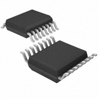
Available in a small TSSOP16 package
s
(
t
c
u
d
o
Pr
Advanced TVs
s
b
O
■
Front projectors
■
LCD Monitors
■
Notebook PCs
■
DVD Players
o
s
b
The STMAV335 is a bi-directional triple (3
channel) Single Pole/Triple Throw (SP3T) highspeed, low-power CMOS TTL-compatible analog
video switch designed for advanced video
applications which demand
superior image
quality. The low ON Resistance (R ON) of the
switch allows inputs to be connected to outputs
without adding propagation delay or generating
additional ground bounce noise.
O
)
■
e
t
e
ol
o
r
P
TSSOP16
e
t
le
Data and control inputs provide the undershoot
clamp diode
■
c
u
d
Description
■
Applications
)
s
t(
STMAV335 is designed for very low cross-talk,
low bit-to-bit skew, high channel-to-channel noise
isolation and low I/O capacitance. The switch
offers very little or practically no attenuation of the
high-speed signals at the outputs, thus preserving
the signal integrity to pass stringent requirements.
Moreover the device reduces the overall BOM
costs by eliminating the need for more costly multi
input-output controllers.
Order Codes
Part Number
Temperature Range
Package
Comments
STMAV335
–40°C to +85°C
TSSOP16
STMAV335TTR
January 2006
Rev. 1
1/21
www.st.com
21
�STMAV335
Contents
1
Summary Description . . . . . . . . . . . . . . . . . . . . . . . . . . . . . . . . . . . . . . . . . . 3
1.1
Functional Description . . . . . . . . . . . . . . . . . . . . . . . . . . . . . . . . . . . . . . . . . . 3
2
Pin Configuration . . . . . . . . . . . . . . . . . . . . . . . . . . . . . . . . . . . . . . . . . . . . . 4
3
Application Diagrams . . . . . . . . . . . . . . . . . . . . . . . . . . . . . . . . . . . . . . . . . . 5
)
s
t(
3.1
Power Supply Sequencing . . . . . . . . . . . . . . . . . . . . . . . . . . . . . . . . . . . . . . . 5
c
u
d
4
Maximum Ratings . . . . . . . . . . . . . . . . . . . . . . . . . . . . . . . . . . . . . . . . . . . . . 6
5
Electrical Characteristics . . . . . . . . . . . . . . . . . . . . . . . . . . . . . . . . . . . . . . . 7
6
AC Loading and Diagrams . . . . . . . . . . . . . . . . . . . . . . . . . . . . . . . . . . . . . . 9
7
Test Circuits . . . . . . . . . . . . . . . . . . . . . . . . . . . . . . . . . . . . . . . . . . . . . . . . . 10
8
Package Mechanical Data . . . . . . . . . . . . . . . . . . . . . . . . . . . . . . . . . . . . . . 17
9
Revision History . . . . . . . . . . . . . . . . . . . . . . . . . . . . . . . . . . . . . . . . . . . . . 20
e
t
le
o
s
b
O
)
s
(
t
c
u
d
o
r
P
e
t
e
l
o
s
b
O
2/21
o
r
P
�STMAV335
1 Summary Description
1
Summary Description
1.1
Functional Description
The STMAV335 is a high bandwidth analog video switch. Its low ON-resistance and low I/O
capacitance result in a very small propagation delay.
The combination of SEL1 and SEL2 is used to either disable or enable the desired video
channel. Refer to the truth table for the selection of the appropriate channels.
Figure 1.
)
s
t(
Functional Diagram
c
u
d
e
t
le
o
r
P
o
s
b
O
)
s
(
t
c
u
d
o
r
P
e
t
e
l
o
s
b
O
3/21
�STMAV335
2 Pin Configuration
2
Pin Configuration
Figure 2.
Pin Configuration (Top View )
SEL1
Y1
Y2
R
Pb1
Pb2
G
Pr/B
Table 1.
Pin Description
Type
SEL1, SEL2
IN
Y/R, Pb/G, Pr/B
Y1, Pb1, Pr1
e
t
e
ol
Y2, Pb2, Pr2
O
)
e
t
le
)
s
t(
c
u
d
o
r
P
Name and Functions
Bus Switch Enable. Tie to VCC through a pull-up resistor. The
minimum value of the resistor is determined by the current-sinking
capability of the driver.
IN/OUT
Analog Video I/Os
IN/OUT
Component 1; Analog Video I/Os
IN/OUT
Component 2; Analog Video I/Os
IN/OUT
RGB or Component 3; Analog Video I/Os
VCC
Power supply
GND
Ground
Table 2.
VCC
SEL2
Y/R
Pb/G
GND
Pr1
Pr2
B
t(s
c
u
d
o
r
P
R, G, B
4/21
16
15
14
13
12
11
10
9
o
s
b
Symbol
s
b
O
1
2
3
4
5
6
7
8
Truth Table
SEL1
SEL2
Selection
0
0
Component = YPbPr1
0
1
Component = YPbPr2
1
0
Component = RGB
1
1
Switch disabled; external pull up resistor recommended
�STMAV335
3
3 Application Diagrams
Application Diagrams
Figure 3.
STMAV335 used in LCD TV as a 3-to-1 analog video switch
)
s
t(
c
u
d
Figure 4.
e
t
le
o
r
P
o
s
b
STMAV335 used in PC as a 1-to-3 analog video switch
O
)
s
(
t
c
u
d
o
r
P
e
t
e
l
o
s
b
O
3.1
Power Supply Sequencing
Proper power-supply sequencing is advised for all CMOS devices. It is recommended to
always apply VCC before applying any signals to the input/output or control pins.
5/21
�STMAV335
4 Maximum Ratings
4
Maximum Ratings
Stressing the device above the rating listed in the “Absolute Maximum Ratings” table may
cause permanent damage to the device. These are stress ratings only and operation of the
device at these or any other conditions above those indicated in the Operating sections of this
specification is not implied. Exposure to Absolute Maximum Rating conditions for extended
periods may affect device reliability. Refer also to the STMicroelectronics SURE Program and
other relevant quality documents.
Table 3.
Absolute Maximum Ratings
)
s
t(
TA = 25°C, VSS= 0V
Symbol
VCC
DC Switch Voltage
VIN
DC Input Voltage
IIK
DC Input Diode Current
IOUT
DC Output Sink Current
ICC/IGND
e
t
le
so
DC V CC/GND Current
TSTG
)
(s
Storage Temperature Range
t
c
u
Ob
o
r
P
Unit
-0.5 to + 7.0
V
-0.5 to + 7.0
V
-0.5 to + 7.0
V
-50
mA
128
mA
±100
mA
-65 to 150
°C
Absolute maximum ratings are those values above which damage to the device may occur.
Functional operation under these conditions is not implied. All voltages are referenced to GND.
d
o
r
P
e
t
e
l
o
s
b
O
6/21
Value
Supply Voltage
VS
Note:
c
u
d
Parameter
�STMAV335
5
5 Electrical Characteristics
Electrical Characteristics
Table 4.
Recommended Operating Conditions
TA = -20 to +70°C, VSS = 0V
Symbol
Parameter (Note 1)
Test Conditions
Min.
Typ.
Max.
Unit
4.0
5.5
V
V
VCC
Power Supply Voltage
VIN
Input Voltage
0
5.5
Output Voltage
0
5.5
V
Switch Control Input
0
5
ns/V
Switch I/O
0
VOUT
tr, tf
Input Rise and Fall Time
TA
Free Air Operating Temperature
VESD
ESD-Human Body Model (HBM) Note 2
Pr
-2
e
t
le
t
c
u
od
-40
)
s
(
DC
ns/V
+85
°C
+2
kV
Max.
Unit
2.0
V
-1.2
V
Note: 1 Unused control inputs must be held HIGH or LOW. They should not float.
2 In accordance with IEC61000-4-2, level 4
Table 5.
TA = -40°C to +85°C
Symbol
O
)
Parameter
Test Conditions
s
(
t
c
Analog Signal Range
u
d
o
VIK
Clamp Diode Voltage
VIH
HIGH Level Input Voltage
VIL
LOW Level Input Voltage
II
IOFF
e
t
e
ol
bs
O
o
s
b
DC Electrical Characteristics
Pr
Input Leakage Current
OFF-STATE Leakage
Current
IIN = -18mA
5
0
Typ.
4.5
4.0-5.5
2.0
V
0.8
V
0 ≤ VIN ≤ 5.5V
5.5
±10
µA
0 ≤ Y/R, Pb/G, Pr/B YX ≤ VCC,
PbX ≤ VCC , PrX ≤ VCC
5.5
±10
µA
R ≤ VCC, G ≤ VCC , B ≤ V CC
VIN = 1.0V, ION = 13mA
4.5
3
7
Ω
VIN = 2.0V, ION = 26mA
4.5
7
10
Ω
5.5
3
µA
5.5
2.5
mA
Switch ON resistance (1)
ICC
Quiescent Supply Current VIN = VCC or GND, IOUT = 0
One input at 3.4V
Other inputs at VCC or GND
Increase in ICC per Input
Min.
4.0-5.5
RON
∆ICC
VCC(V)
Note: 1 Measured by the voltage drop between Y/R, Pb/G, Pr/B and YX/R, PbX/G, PrX/B pins at the
indicated current through the switch. ON Resistance is determined by the lower of the voltages
on the two.
7/21
�STMAV335
5 Electrical Characteristics
Table 6.
AC Electrical Characteristics
TA = -40°C to +85°C, CL = 20pF, RU = RD = 75Ω
Symbol
Parameter
VCC = 4.5 - 5.5V
Test conditions
Min.
Output Enable Time Select to Bus YX/
R, PbX/G, PrX/B
tPZH, tPZL
Output Enable Time Select to Bus Y/R,
Pb/G, Pr/B
Output Disable Time Select to Bus YX/
R, PbX/G, PrX/B
tPHZ, tPLZ
Output Disable Time, Output Enable
time OE_N to Bus A, B/C
BW
XTALK
DP
Differential Phase
PIRR
CI/O
Ob
CON
8/21
5.5
5.5
)
s
(
ns
ns
300
-58
)
s
(
ct
u
d
o
l
o
s
b
O
-
r
P
e
Test Conditions
Control Pin Input Capacitance
VCC = 5.0V
Input/Output Capacitance
Port: Y/R, Pb/G, Pr/B
VCC, SEL1,
let
Input/Output Capacitance
Port: YX/R, PbX/G, PrX/B
SEL2 = 5.0 V
Switch On Capacitance
Except
SEL1,SEL2=5.0
t
c
u
5.5
d
o
r
Min.
MHz
dB
P
e
et
10 MHz
Parameter
so
5.2
f = 3.58 MHz
RL = 150Ω
TA = 25°C, f = 1MHz
CIN
VI = 7V for tPLZ
VI = OPEN for tPHZ
f = 3.58 MHz
RL = 150Ω
Capacitance
Symbol
5.6
RL = 150Ω
OFF Isolation
Table 7.
5.1
RL = 150Ω, 10 MHz
Differential Gain
Unit
Max.
5.7
RIN = 10Ω
DG
Min.
5.2
TA = 25°C
Crosstalk
Max.
VI = 7V for tPZL
VI = OPEN for tPHZ
RL = 150Ω
-3dB Bandwidth
Typ.
VCC = 4.0V
0.64
%
0.1
Deg.
-60
dB
Typ.
Max.
Unit
3
pF
7
pF
5
pF
12
pF
VCC = 5.0V,
�STMAV335
6
6 AC Loading and Diagrams
AC Loading and Diagrams
Figure 5.
AC Test Circuit
V
I
RU
FROM OUTPUT
UNDER TEST
20 pF
L
Figure 6.
o
s
b
O
)
AC Waveforms
s
(
t
c
tf = 2.5ns
u
d
o
90%
r
P
e
ENABLE
INPUT
s
b
O
t
e
l
o
c
u
d
o
r
P
RD 75 Ω
e
t
le
C
)
s
t(
t r = 2.5ns
3.0V
90%
1.5V
1.5V
10%
10%
tPZL
GND
tPLZ
OUTPUT
1.5 V
tPZH
VOL + 0.3V
VOL
t PHZ
OUTPUT
1.5 V
VOH
VOH – 0.3V
9/21
�STMAV335
7 Test Circuits
7
Test Circuits
Figure 7.
Test Circuit to measure the on-resistance of the switch
)
s
t(
c
u
d
e
t
le
o
s
b
O
)
s
(
t
c
u
d
o
r
P
e
t
e
l
o
s
b
O
10/21
o
r
P
�STMAV335
Figure 8.
7 Test Circuits
Enable/Disable Circuit and Timing Diagram
)
s
t(
c
u
d
e
t
le
o
r
P
o
s
b
O
)
s
(
t
c
u
d
o
r
P
e
t
e
l
o
s
b
O
Table 8.
Test Circuit
Test
VCC
RL
CL
VY1
VPb1
VPr1
4.75V ± 0.75V
4.75V ± 0.75V
4.75V ± 0.75V
75
75
75
20
20
20
GND
GND
VCC
GND
VCC
VCC
4.75V ± 0.75V
Disable Time
4.75V ± 0.75V
(tpLZ, tpHZ)
4.75V ± 0.75V
75
75
75
20
20
20
GND
GND
VCC
GND
VCC
Enable time
(tpZL, tpZH)
GND
GND
GND
GND
VCC
GND
GND
Note: 1 CL includes probe and jig capacitance.
2 All input pulses are supplied by generators having the following characteristics: PRR ≤ 10MHz,
ZO = 50Ω, tr, tf = 2.5ns.
3 The outputs are measured one at a time, with one transition per measurement.
11/21
�STMAV335
7 Test Circuits
Differential gain and phase are measured at the output of the ON channel. For example, when
SEL1, SEL2 = 0 and Y is the input, the output is measured at Y1.
Figure 9.
Differential Gain/Phase Measurement Test Circuit
)
s
t(
c
u
d
e
t
le
o
s
b
O
)
s
(
t
c
u
d
o
r
P
e
t
e
l
o
s
b
O
12/21
o
r
P
�STMAV335
7 Test Circuits
Frequency response is measured at the output of the ON channel. For example, when
SEL1,SEL2 = 0, and Y is the input, the output is measured at Y1. All unused analog I/O ports
are left open.
Figure 10. Test Circuit for frequency response (BW)
)
s
t(
c
u
d
e
t
le
o
r
P
o
s
b
O
)
s
(
t
c
u
d
o
r
P
e
t
e
l
o
s
b
O
13/21
�STMAV335
7 Test Circuits
Crosstalk is measured at the output of the non-adjacent ON channel. For example, when
SEL1,SEL2 = 0, and Y is the input, the output is measured at Pb1. All unused analog input
ports (Pb,Pr) and output ports (PbX,PrX) are connected to GND through 10Ω and 50Ω pulldown resistors respectively.
Figure 11. Crosstalk Test Circuit
)
s
t(
c
u
d
e
t
le
o
s
b
O
)
s
(
t
c
u
d
o
r
P
e
t
e
l
o
s
b
O
Note:
14/21
50Ω termination resistor is needed for the network analyzer.
o
r
P
�STMAV335
7 Test Circuits
Off-Isolation is measured at the output of the OFF channel. For example, when SEL1=0,
SEL2=VCC, and Y is the input, the output is measured at Y1. All unused analog input ports are
left open, and output ports are connected to GND through 50Ω pull-down resistors.
Figure 12. Off-Isolation Test Circuit
)
s
t(
c
u
d
e
t
le
o
r
P
o
s
b
O
)
s
(
t
c
u
d
o
r
P
e
t
e
l
o
s
b
O
Note:
50Ω termination resistor is needed for the network analyzer.
15/21
�STMAV335
7 Test Circuits
Figure 13. ESD protection circuit for Input side of I/O pin
)
s
t(
c
u
d
Figure 14. ESD protection circuit for Output side of I/O pin
e
t
le
o
s
b
O
)
s
(
t
c
u
d
o
r
P
e
t
e
l
o
Figure 15. ESD protection circuit for SEL1, SEL2 inputs
s
b
O
16/21
o
r
P
�STMAV335
8
8 Package Mechanical Data
Package Mechanical Data
In order to meet environmental requirements, ST offers these devices in ECOPACK®
packages. These packages have a Lead-free second level interconnect . The category of
second Level Interconnect is marked on the package and on the inner box label, in compliance
with JEDEC Standard JESD97. The maximum ratings related to soldering conditions are also
marked on the inner box label. ECOPACK is an ST trademark. ECOPACK specifications are
available at: www.st.com.
)
s
t(
c
u
d
e
t
le
o
r
P
o
s
b
O
)
s
(
t
c
u
d
o
r
P
e
t
e
l
o
s
b
O
17/21
�STMAV335
8 Package Mechanical Data
TSSOP16 MECHANICAL DATA
mm
DIM.
MIN.
inch
TYP.
MAX.
A
MIN.
TYP.
MAX.
1.1
0.433
A1
0.05
0.10
0.15
0.002
0.004
0.006
A2
0.85
0.9
0.95
0.335
0.354
0.374
b
0.19
0.30
0.0075
c
0.09
0.20
0.0035
D
4.9
5
5.1
0.193
E
6.25
6.4
6.5
0.246
E1
4.3
4.4
4.48
e
K
0o
4o
L
0.50
0.60
Ob
)-
0.70
od
0.197
r
P
e
0.256
0.173
0.176
0o
4o
8o
0.020
0.024
0.028
r
P
e
let
o
s
b
u
d
o
A2
A1
b
O
e
K
c
E1
PIN 1 IDENTIFICATION
1
18/21
L
E
D
0.201
0.252
s
(
t
c
A
0.0079
0.0256 BSC
so
8o
uc
let
0.169
0.65 BSC
)
s
t(
0.0118
�STMAV335
8 Package Mechanical Data
Tape & Reel TSSOP16 MECHANICAL DATA
mm.
inch
DIM.
MIN.
TYP
A
MAX.
MIN.
TYP.
330
MAX.
C
12.8
D
N
12.992
13.2
0.504
0.519
20.2
0.795
60
2.362
)
s
t(
T
uc
22.4
Ao
6.7
6.9
0.264
Bo
5.3
5.5
0.209
Ko
1.6
1.8
0.063
Po
3.9
4.1
P
7.9
8.1
bs
ol
e
t
e
Pr
od
0.882
0.272
0.217
0.071
0.153
0.161
0.311
0.319
O
)
s
(
t
c
u
d
o
r
P
e
t
e
l
o
s
b
O
19/21
�STMAV335
9 Revision History
9
Revision History
Date
Revision
23-Jan-2006
1
Description of Change
First Release
)
s
t(
c
u
d
e
t
le
o
s
b
O
)
s
(
t
c
u
d
o
r
P
e
t
e
l
o
s
b
O
20/21
o
r
P
�STMAV335
9 Revision History
)
s
t(
c
u
d
e
t
le
o
r
P
o
s
b
O
)
s
(
t
c
u
d
o
r
P
e
t
e
l
o
s
b
O
Information furnished is believed to be accurate and reliable. However, STMicroelectronics assumes no responsibility for the consequences
of use of such information nor for any infringement of patents or other rights of third parties which may result from its use. No license is granted
by implication or otherwise under any patent or patent rights of STMicroelectronics. Specifications mentioned in this publication are subject
to change without notice. This publication supersedes and replaces all information previously supplied. STMicroelectronics products are not
authorized for use as critical components in life support devices or systems without express written approval of STMicroelectronics.
The ST logo is a registered trademark of STMicroelectronics.
All other names are the property of their respective owners
© 2006 STMicroelectronics - All rights reserved
STMicroelectronics group of companies
Australia - Belgium - Brazil - Canada - China - Czech Republic - Finland - France - Germany - Hong Kong - India - Israel - Italy - Japan Malaysia - Malta - Morocco - Singapore - Spain - Sweden - Switzerland - United Kingdom - United States of America
www.st.com
21/21
�