1. 物料型号:
- 型号:STN83003
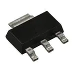
- 封装:SOT-223
- 包装:Tape & reel
2. 器件简介:
- STN83003是一款高电压快速开关NPN功率晶体管,采用高压多外延平面技术制造,具有高开关速度和中等电压能力。它使用带有平面边缘终止的蜂窝发射极结构,在保持宽RBSOA的同时提高开关速度。
3. 引脚分配:
- SOT-223塑料封装适用于表面贴装电路。
4. 参数特性:
- 绝对最大额定值:
- VCES:700V
- VCEO:400V
- Ic:1.5A
- ICM:3A
- 1B:0.75A
- IBM:1.5A
- Ptot:1.6W
- Tstg:-65至150°C
- TJ:150°C
- 热数据:
- Rthj-amb:最大78°C/W(器件安装在1cm²的PCB面积上)
5. 功能详解:
- STN83003专为紧凑型荧光灯的新解决方案设计,与互补的PNP晶体管STN93003配对使用。
6. 应用信息:
- 应用于荧光灯电子镇流器和开关模式电源。
7. 封装信息:
- 提供ECOPACK®封装,符合JEDEC标准JESD97,无铅二级互连。
- SOT-223机械数据:
- A:最小1.80mm,典型0.071英寸
- B:最小0.60mm,典型0.027英寸
- B1:最小2.90mm,典型0.118英寸
- C:最小0.24mm,典型0.010英寸
- D:最小6.30mm,典型0.256英寸
- E:最小3.30mm,典型0.138英寸
- H:最小6.70mm,典型0.276英寸
- V:10英寸


 工商网监
湘ICP备2023018690号
工商网监
湘ICP备2023018690号
