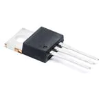
STP140N8F7
N-channel 80 V, 3.5 mΩ typ., 90 A STripFET™ F7
Power MOSFET in a TO-220 package
Datasheet - production data
Features
Order code
VDS
RDS(on) max.
ID
PTOT
STP140N8F7
80 V
4.3 mΩ
90 A
200 W
Among the lowest RDS(on) on the market
Excellent figure of merit (FoM)
Low Crss/Ciss ratio for EMI immunity
High avalanche ruggedness
Applications
Figure 1: Internal schematic diagram
Switching applications
Description
This N-channel Power MOSFET utilizes
STripFET™ F7 technology with an enhanced
trench gate structure that results in very low onstate resistance, while also reducing internal
capacitance and gate charge for faster and more
efficient switching.
D(2, TAB)
G(1)
Table 1: Device summary
Order code
Marking
Package
Packaging
STP140N8F7
140N8F7
TO-220
Tube
S(3)
AM01475v1_Tab
October 2014
DocID026822 Rev 2
This is information on a product in full production.
1/13
www.st.com
�Contents
STP140N8F7
Contents
1
Electrical ratings ............................................................................. 3
2
Electrical characteristics ................................................................ 4
2.1
Electrical characteristics (curves) ...................................................... 6
3
Test circuits ..................................................................................... 8
4
Package mechanical data ............................................................... 9
4.1
5
2/13
TO-220 type A package information................................................ 10
Revision history ............................................................................ 12
DocID026822 Rev 2
�STP140N8F7
1
Electrical ratings
Electrical ratings
Table 2: Absolute maximum ratings
Symbol
Parameter
Value
Unit
VDS
Drain-source voltage
80
V
VGS
Gate-source voltage
± 20
V
(1)
A
ID
Drain current (continuous) at TC = 25 °C
ID
90
Drain current (continuous) at TC = 100 °C
90
A
IDM(2)
Drain current (pulsed)
360
A
PTOT
Total dissipation at TC = 25 °C
200
W
EAS(3)
Single pulse avalanche energy
515
mJ
Tj
Operating junction temperature
- 55 to 175
°C
Tstg
Storage temperature
Notes:
(1)Limited
(2)Pulse
by package
width is limited by safe operating area
(3)Starting
Tj =25 °C, Id = 18.5 A, Vdd = 50 V
Table 3: Thermal data
Symbol
Parameter
Value
Unit
Rthj-case
Thermal resistance junction-case
0.75
°C/W
Rthj-amb
thermal resistance junction-ambient
62.5
°C/W
DocID026822 Rev 2
3/13
�Electrical characteristics
2
STP140N8F7
Electrical characteristics
(TCASE = 25 °C unless otherwise specified)
Table 4: On/off states
Symbol
V(BR)DSS
Parameter
Test conditions
Drain-source breakdown
voltage
VGS = 0, ID = 250 µA
Min.
Typ.
Max.
80
Unit
V
VGS = 0, VDS = 80 V
1
µA
VGS = 0, VDS = 80 V, TJ=125
°C
10
µA
±100
nA
4.5
V
3.5
4.3
mΩ
Min.
Typ.
Max.
Unit
-
6340
-
pF
-
1195
-
pF
-
105
-
pF
-
96
-
nC
-
30
-
nC
-
26
-
nC
Min.
Typ.
Max.
Unit
-
26
-
ns
-
51
-
ns
-
82
-
ns
-
44
-
ns
IDSS
Zero gate voltage
Drain current
IGSS
Gate-source leakage
current
VDS = 0, VGS = ±20 V
VGS(th)
Gate threshold voltage
VDS = VGS, ID = 250 µA
RDS(on)
Static drain-source onresistance
VGS=10 V, ID = 45 A
2.5
Table 5: Dynamic
Symbol
Parameter
Ciss
Input capacitance
Coss
Output capacitance
Crss
Reverse transfer
capacitance
Qg
Total gate charge
Qgs
Gate-source charge
Qgd
Gate-drain charge
Test conditions
VGS = 0, VDS = 40 V, f = 1
MHz
VDD = 40 V, ID = 64 A,
VGS = 10 V
Table 6: Switching times
Symbol
td(on)
tr
td(off)
tf
4/13
Parameter
Test conditions
Turn-on delay
time
Rise time
Turn-off-delay
time
VDD = 40 V, ID = 45 A RG=4.7 Ω, VGS =
10 V
Fall time
DocID026822 Rev 2
�STP140N8F7
Electrical characteristics
Table 7: Source drain diode
Symbol
ISD
Parameter
Test conditions
Source-drain current
Min.
Typ.
Max.
Unit
-
90
A
ISDM(1)
Source-drain current (pulsed)
-
360
A
VSD (2)
Forward on voltage
VGS = 0, ISD = 90 A
-
1.2
V
trr
Reverse recovery time
-
58
ns
Qrr
Reverse recovery charge
-
92
nC
IRRM
Reverse recovery current
ISD = 64 A, di/dt = 100 A/µs,
VDD = 60 V
Tj = 150 °C
-
3.2
A
Notes:
(1)Pulse
width is limited by safe operating area
(2)Pulse
test: pulse duration = 300 µs, duty cycle 1.5%
DocID026822 Rev 2
5/13
�Electrical characteristics
2.1
STP140N8F7
Electrical characteristics (curves)
Figure 3: Thermal impedance
Figure 2: Safe operating area
K
GIPD130920130848MT
ID
(A)
δ= 0.5
100
0.2
10
100µs
Operation in this area is
10
-1
0.05
Limited by max RDS(on)
0.02
0.01
1ms
Tj=175°C
Tc=25°C
1
10
10
1
-2
10
V DS(V)
Figure 4: Output characteristics
-7
10
-6
10
-5
10
-4
10
-3
10
-2 10 -1 tp(s)
Figure 5: Transfer characteristics
GIPD130920130919MT
ID
(A)
Single pulse
10ms
Sinlge
pulse
0.1
0.1
0.1
ID
(A)
V GS= 10V
300
300
7V
250
V DS= 2V
250
6V
200
200
150
150
5V
100
100
50
50
4V
0
0
2
4
6
8
0
0
V DS(V)
Figure 6: Normalized V(BR)DSS vs.
temperature
V (BR)DSS
3
4
5
6
7
8
9 V GS(V)
Figure 7: Static drain-source on resistance
R DS(on)
3.52
ID= 250µA
1.04
2
1
1.02
V GS= 10V
3.51
1
3.50
0.98
3.49
0.96
0.94
-75
6/13
3.48
-25
0 25
75
125
175 T J(°C)
DocID026822 Rev 2
20
30
40
50
60
70
80
90 ID(A)
�STP140N8F7
Electrical characteristics
Figure 8: Gate charge vs. gate-source voltage
Figure 9: Capacitance variations
V GS
(V)
C
(pF)
8000
12
7000
10
C iss
6000
8
5000
6
4000
3000
4
2000
2
0
1000
0
20
40
80
60
0
0
100 Q g(nC)
10
20
30
40
50
60
C oss
C rss
70 V DS(V)
Figure 11: Normalized on resistance vs.
temperature
Figure 10: Normalized gate threshold voltage
vs. temperature
V GS(th)
R DS(on)
V GS= 10V
1.2
1.8
ID= 250µA
1.6
1
1.4
1.2
0.8
1
0.8
0.6
0.6
0.4
-75
-25
0 25
75
125
0.4
-75
175 T J(°C)
-25
0 25
75
125
175 T J(°C)
Figure 12: Source-drain diode forward characteristics
V SD
T J= -55°C
1.1
1
0.9
T J= 25°C
0.8
T J= 175°C
0.7
0.6
20
30
40
50
60
DocID026822 Rev 2
70
80
90
ID(A)
7/13
�Test circuits
3
STP140N8F7
Test circuits
Figure 13: Switching times test circuit for
resistive load
Figure 15: Test circuit for inductive load
switching and diode recovery times
Figure 17: Unclamped inductive waveform
8/13
DocID026822 Rev 2
Figure 14: Gate charge test circuit
Figure 16: Unclamped inductive load test
circuit
Figure 18: Switching time waveform
�STP140N8F7
4
Package mechanical data
Package mechanical data
In order to meet environmental requirements, ST offers these devices in different grades of
ECOPACK® packages, depending on their level of environmental compliance. ECOPACK ®
specifications, grade definitions and product status are available at: www.st.com.
ECOPACK® is an ST trademark.
DocID026822 Rev 2
9/13
�Package mechanical data
4.1
STP140N8F7
TO-220 type A package information
Figure 19: TO-220 type A package outline
10/13
DocID026822 Rev 2
�STP140N8F7
Package mechanical data
Table 8: TO-220 type A mechanical data
mm
Dim.
Min.
Typ.
Max.
A
4.40
4.60
b
0.61
0.88
b1
1.14
1.70
c
0.48
0.70
D
15.25
15.75
D1
1.27
E
10
10.40
e
2.40
2.70
e1
4.95
5.15
F
1.23
1.32
H1
6.20
6.60
J1
2.40
2.72
L
13
14
L1
3.50
3.93
L20
16.40
L30
28.90
ÆP
3.75
3.85
Q
2.65
2.95
DocID026822 Rev 2
11/13
�Revision history
5
STP140N8F7
Revision history
Table 9: Document revision history
12/13
Date
Revision
Changes
25-Aug-2014
1
First release.
09-Oct-2014
2
Updated Figure 3: "Thermal impedance"
DocID026822 Rev 2
�STP140N8F7
IMPORTANT NOTICE – PLEASE READ CAREFULLY
STMicroelectronics NV and its subsidiaries (“ST”) reserve the right to make changes, corrections, enhancements, modifications, and
improvements to ST products and/or to this document at any time without notice. Purchasers should obtain the latest relevant information on ST
products before placing orders. ST products are sold pursuant to ST’s terms and conditions of sale in place at the time of order
acknowledgement.
Purchasers are solely responsible for the choice, selection, and use of ST products and ST assumes no liability for application assistance or the
design of Purchasers’ products.
No license, express or implied, to any intellectual property right is granted by ST herein.
Resale of ST products with provisions different from the information set forth herein shall void any warranty granted by ST for such product.
ST and the ST logo are trademarks of ST. All other product or service names are the property of their respective owners.
Information in this document supersedes and replaces information previously supplied in any prior versions of this document.
© 2014 STMicroelectronics – All rights reserved
DocID026822 Rev 2
13/13
�
很抱歉,暂时无法提供与“STP140N8F7”相匹配的价格&库存,您可以联系我们找货
免费人工找货- 国内价格
- 1+15.57360
- 10+13.21920
- 50+11.27520
- 国内价格 香港价格
- 1+29.537771+3.81774
- 50+14.6853050+1.89807
- 100+13.24804100+1.71230
- 500+10.72791500+1.38658
- 1000+9.918051000+1.28190
- 2000+9.237162000+1.19390
- 5000+8.500985000+1.09875
- 10000+8.4882110000+1.09710
- 国内价格 香港价格
- 1+25.966121+3.35610
- 5+23.255855+3.00580
- 国内价格
- 50+18.67722
- 250+18.30441
- 国内价格
- 1+24.26972
- 5+21.74502
- 14+21.01204
- 国内价格
- 1+12.11100
- 100+10.25200
- 1000+9.91100