STP45NE06
STP45NE06FP
®
N - CHANNEL 60V - 0.022Ω - 45A - TO-220/TO-220FP
STripFET POWER MOSFET
PRELIMINARY DATA
TYPE
V DSS
R DS(on)
ID
STP45NE06
STP45NE06FP
60 V
60 V
< 0.028 Ω
< 0.028 Ω
45 A
25 A
TYPICAL RDS(on) = 0.022 Ω
EXCEPTIONAL dv/dt CAPABILITY
100% AVALANCHE TESTED
LOW GATE CHARGE 100 oC
APPLICATION ORIENTED
CHARACTERIZATION
■
■
■
■
■
3
1
DESCRIPTION
This Power Mosfet is the latest development of
SGS-THOMSON unique "Single Feature Size "
strip-based process. The resulting transistor
shows extremely high packing density for low onresistance, rugged avalance characteristics and
less critical alignment steps therefore a remarkable manufacturing reproducibility.
1
c
u
d
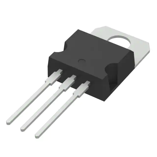
TO-220
e
t
le
)
s
t(
2
TO-220FP
o
r
P
INTERNAL SCHEMATIC DIAGRAM
o
s
b
O
-
APPLICATIONS
■ HIGH CURRENT, HIGH SPEED SWITCHING
■ SOLENOID AND RELAY DRIVERS
■ MOTOR CONTROL, AUDIO AMPLIFIERS
■ DC-DC & DC-AC CONVERTERS
)
s
(
ct
3
2
u
d
o
ABSOLUTE MAXIMUM RATINGS
r
P
e
Symbol
V DGR
bs
O
ID
ID
IDM (•)
P tot
60
V
Drain- gate Voltage (R GS = 20 kΩ)
60
V
± 20
Gate-source Voltage
45
25
A
Drain Current (continuous) at T c = 100 o C
31
17.5
A
180
180
A
Drain Current (pulsed)
o
Total Dissipation at T c = 25 C
100
35
W
Derating Factor
0.67
0.23
W/ o C
2000
V
dv/dt
Peak Diode Recovery voltage slope
Storage Temperature
Max. Operating Junction Temperature
(•) Pulse width limited by safe operating area
June 1998
V
Drain Current (continuous) at T c = 25 o C
Insulation Withstand Voltage (DC)
Tj
Unit
STP45NE06FP
Drain-source Voltage (V GS = 0)
V ISO
T stg
Value
STP45NE06
t
e
l
o
V DS
V GS
Parameter
7
V/ns
-65 to 175
o
C
175
o
C
(1) ISD ≤ 20 A, di/dt ≤ 300 A/µs, VDD ≤ V(BR)DSS, Tj ≤ TJMAX
1/6
�STP45NE06/FP
THERMAL DATA
R thj-case
Thermal Resistance Junction-case
R thj-amb
R thc-sink
Tl
Thermal Resistance Junction-ambient
Max
Thermal Resistance Case-sink
Typ
Maximum Lead Temperature For Soldering Purpose
TO-220
TO-220FP
1.5
4.28
Max
62.5
0.5
300
o
C/W
o
C/W
C/W
o
C
o
AVALANCHE CHARACTERISTICS
Symbol
Parameter
I AR
Avalanche Current, Repetitive or Not-Repetitive
(pulse width limited by T j max)
E AS
Single Pulse Avalanche Energy
(starting T j = 25 o C, I D = I AR , VDD = 25V)
Max Value
Unit
45
A
150
mJ
Min.
Typ.
)
s
t(
60
od
ELECTRICAL CHARACTERISTICS (Tcase = 25 oC unless otherwise specified)
OFF
Symbol
V (BR)DSS
Parameter
Drain-source
Breakdown Voltage
Test Conditions
I D = 250 µA
I DSS
Zero Gate Voltage
V DS = Max Rating
Drain Current (V GS = 0) V DS = Max Rating
I GSS
Gate-body Leakage
Current (V DS = 0)
Symbol
Parameter
(s)
Gate Threshold
Voltage
V DS = VGS
R DS(on)
Static Drain-source On
Resistance
V GS = 10V
DYNAMIC
s
b
O
g fs (∗)
C iss
C oss
C rss
o
s
b
O
-
ct
u
d
o
ID = 250 µA
r
P
e
Parameter
Pr
Forward
Transconductance
V DS > I D(on) x R DS(on)max
Input Capacitance
Output Capacitance
Reverse Transfer
Capacitance
V DS = 25 V
f = 1 MHz
I D =22.5 A
V GS = 0
V
1
10
µA
µA
± 100
nA
Typ.
Max.
Unit
2
3
4
V
0.022
0.028
Ω
45
Test Conditions
Unit
Min.
I D = 22.5A
On State Drain Current V DS > I D(on) x R DS(on)max
V GS = 10 V
t
e
l
o
Symbol
e
t
le
Test Conditions
V GS(th)
ID(on)
T c = 125 o C
V GS = ± 20 V
ON (∗)
2/6
VGS = 0
uc
Max.
A
Min.
Typ.
15
30
2700
350
70
Max.
Unit
S
3600
480
100
pF
pF
pF
�STP45NE06/FP
ELECTRICAL CHARACTERISTICS (continued)
SWITCHING ON
Symbol
Parameter
Test Conditions
t d(on)
tr
Turn-on Time
Rise Time
V DD = 30 V
R G =4.7 Ω
Qg
Q gs
Q gd
Total Gate Charge
Gate-Source Charge
Gate-Drain Charge
V DD = 48 V
Min.
I D = 22.5 A
V GS = 10 V
I D = 45A
V GS = 10 V
Typ.
Max.
Unit
30
100
40
135
ns
ns
60
18
17
80
nC
nC
nC
Typ.
Max.
Unit
20
45
70
30
61
95
ns
ns
ns
SWITCHING OFF
Symbol
t r(Voff)
tf
tc
Parameter
Off-voltage Rise Time
Fall Time
Cross-over Time
Test Conditions
Min.
V DD = 48 V I D = 45 A
R G =4.7 Ω V GS = 10 V
SOURCE DRAIN DIODE
Symbol
Parameter
Test Conditions
I SD
I SDM (•)
Source-drain Current
Source-drain Current
(pulsed)
V SD (∗)
Forward On Voltage
I SD = 45 A
Reverse Recovery
Time
Reverse Recovery
Charge
Reverse Recovery
Current
I SD = 45 A
V DD = 30 V
t rr
Q rr
I RRM
(∗) Pulsed: Pulse duration = 300 µs, duty cycle 1.5 %
(•) Pulse width limited by safe operating area
)
s
(
ct
Min.
r
P
e
t
le
VGS = 0
di/dt = 100 A/µs
o
T j = 150 C
b
O
-
so
uc
Typ.
od
)
s
t(
Max.
Unit
45
180
A
A
1.5
V
70
ns
210
µC
6
A
u
d
o
r
P
e
t
e
l
o
s
b
O
3/6
�STP45NE06/FP
TO-220 MECHANICAL DATA
mm
DIM.
MIN.
inch
TYP.
MAX.
MIN.
MAX.
A
4.40
4.60
0.173
0.181
C
1.23
1.32
0.048
0.051
D
2.40
2.72
0.094
D1
0.107
1.27
0.050
E
0.49
0.70
0.019
0.027
F
0.61
0.88
0.024
0.034
F1
1.14
1.70
0.044
0.067
F2
1.14
1.70
0.044
0.067
G
4.95
5.15
0.194
0.203
G1
2.4
2.7
0.094
0.106
H2
10.0
10.40
0.393
0.409
16.4
0.645
13.0
14.0
0.511
L5
2.65
2.95
0.104
L6
15.25
15.75
0.600
L7
6.2
6.6
0.244
L9
3.5
3.93
0.137
DIA.
3.75
3.85
D1
u
d
o
so
0.620
0.260
0.154
0.147
b
O
-
0.151
L2
G
G1
F1
r
P
e
H2
C
)
s
(
ct
e
t
le
o
r
P
0.551
0.116
D
A
L4
t
e
l
o
c
u
d
)
s
t(
E
L2
F
Dia.
F2
s
b
O
TYP.
L5
L9
L7
L6
4/6
L4
P011C
�STP45NE06/FP
TO-220FP MECHANICAL DATA
mm
DIM.
MIN.
inch
TYP.
MAX.
MIN.
TYP.
MAX.
A
4.4
4.6
0.173
0.181
B
2.5
2.7
0.098
0.106
D
2.5
2.75
0.098
0.108
E
0.45
0.7
0.017
0.027
F
0.75
1
0.030
0.039
F1
1.15
1.7
0.045
0.067
F2
1.15
1.7
0.045
0.067
G
4.95
5.2
0.195
0.204
G1
2.4
2.7
0.094
H
10
10.4
0.393
L2
16
28.6
30.6
1.126
L4
9.8
10.6
0.385
L6
15.9
16.4
0.626
L7
9
9.3
0.354
Ø
3
3.2
0.417
0.366
0.118
0.126
D
E
b
O
-
1.204
0.645
so
L3
L6
L7
G
G1
¯
F2
H
s
b
O
t
e
l
o
o
r
P
0.409
F
B
r
P
e
e
t
le
F1
A
)
s
(
ct
u
d
o
c
u
d
0.630
L3
)
s
t(
0.106
1 2 3
L2
L4
5/6
�STP45NE06/FP
c
u
d
e
t
le
)
s
(
ct
)
s
t(
o
r
P
o
s
b
O
-
u
d
o
r
P
e
t
e
l
o
s
b
O
Information furnished is believed to be accurate and reliable. However, STMicroelectronics assumes no responsibility for the consequences
of use of such information nor for any infringement of patents or other rights of third parties which may result from its use. No license is
granted by implication or otherwise under any patent or patent rights of STMicroelectronics. Specification mentioned in this publication are
subject to change without notice. This publication supersedes and replaces all information previously supplied. STMicroelectronics products
are not authorized for use as critical components in life support devices or systems without express written approval of STMicroelectronics.
The ST logo is a trademark of STMicroelectronics
© 1998 STMicroelectronics – Printed in Italy – All Rights Reserved
STMicroelectronics GROUP OF COMPANIES
Australia - Brazil - Canada - China - France - Germany - Italy - Japan - Korea - Malaysia - Malta - Mexico - Morocco - The Netherlands Singapore - Spain - Sweden - Switzerland - Taiwan - Thailand - United Kingdom - U.S.A.
.
6/6
�
很抱歉,暂时无法提供与“STP45NE06”相匹配的价格&库存,您可以联系我们找货
免费人工找货