STP80NF55L-06

STP80NF55L-06

  • 厂商:

    STMICROELECTRONICS(意法半导体)

  • 封装:

    SOT78

  • 描述:

    N沟道,55V,80A

  • 详情介绍
  • 数据手册
  • 价格&库存
STP80NF55L-06 数据手册
® STP80NF55L-06 N - CHANNEL 55V - 0.005 Ω - 80A TO-220 STripFET™ POWER MOSFET TYPE STP80NF55L-06 s s s V DSS 55 V R DS( on ) < 0.0065 Ω ID 80 A TYPICAL RDS(on) = 0.005 Ω LOW THRESHOLD DRIVE LOGIC LEVEL DEVICE DESCRIPTION This Power MOSFET is the latest development of STMicroelectronics unique ”Single Feature Size™” strip-based process. The resulting transistor shows extremely high packing density for low on-resistance, rugged avalanche characteristics and less critical alignment steps therefore a remarkable manufacturing reproducibility. APPLICATIONS s HIGH CURRENT, HIGH SPEED SWITCHING s SOLENOID AND RELAY DRIVERS s MOTOR CONTROL, AUDIO AMPLIFIERS s DC-DC & DC-AC CONVERTERS 3 1 2 TO-220 I NTERNAL SCHEMATIC DIAGRAM ABSOLUTE MAXIMUM RATINGS Symb ol V DS V DGR VGS ID ID I DM ( •) P tot E AS ( 1 ) T st g Tj Parameter Drain-source Voltage (VGS = 0) Drain- gate Voltage (R GS = 20 k Ω ) G ate-source Voltage Drain Current (continuous) at Tc = 25 oC Drain Current (continuous) at Tc = 100 o C Drain Current (pulsed) T otal Dissipation at Tc = 25 C Derating Factor Single Pulse Avalanche Energy Storage Temperature Max. Operating Junction Temperature o Value 55 55 ± 20 80 57 320 210 1.4 1 -65 to 175 175 ( 1) starting Tj = 25 oC, ID =40A , VDD = 30V Unit V V V A A A W W /o C J o o C C (•) Pulse width limited by safe operating area October 1999 1/8 STP80NF55L-06 THERMAL DATA R thj -case R thj -amb Tl Thermal Resistance Junction-case Max Thermal Resistance Junction-ambient Max Maximum Lead Temperature F or Soldering Purpose 0.71 62.5 300 o o C/W C/W o C ELECTRICAL CHARACTERISTICS (Tcase = 25 oC unless otherwise specified) OFF Symbo l V (BR)DSS I DSS IGSS Parameter Drain-source Breakdown Voltage Test Con ditions I D = 250 µ A V GS = 0 Min. 55 1 10 ± 100 Typ. Max. Unit V µA µA nA V DS = Max Rating Zero Gate Voltage Drain Current (V GS = 0) V DS = Max Rating Gate-body Leakage Current (VDS = 0) V GS = ± 20 V T c =125 oC ON (∗) Symbo l V GS(th) R DS(on) I D(o n) Parameter Gate Threshold Voltage V DS = V GS Static Drain-source On Resistance On State Drain Current V GS = 10 V V GS = 5 V Test Con ditions ID = 250 µ A ID = 40 A I D = 40 A 80 Min. 1 Typ. 1.6 Max. 2.5 Unit V Ω Ω A 0.005 0.0065 0.0055 0.008 V DS > ID(o n) x R DS(on )ma x V GS = 10 V DYNAMIC Symbo l g f s (∗ ) C iss C os s C rss Parameter Forward Transconductance Input Capacitance Output Capacitance Reverse Transfer Capacitance Test Con ditions V DS > ID(o n) x R DS(on )ma x V DS = 25 V f = 1 MHz I D =18 A V GS = 0 Min. Typ. 20 7600 990 270 Max. Unit S pF pF pF 2/8 STP80NF55L-06 ELECTRICAL CHARACTERISTICS (continued) SWITCHING ON Symbo l t d(on) tr Qg Q gs Q gd Parameter Turn-on Delay T ime Rise Time Total G ate Charge Gate-Source Charge Gate-Drain Charge Test Con ditions V DD = 27 V I D = 40 A R G = 4.7 Ω V GS = 4.5 V (Resistive Load, see fig. 3) V DD = 44 V ID = 80 A V GS = 5 V Min. Typ. 75 300 97 25 46 100 Max. Unit ns ns nC nC nC SWITCHING OFF Symbo l t d(of f) tf t d(of f) tf tc Parameter Turn-off Delay T ime Fall T ime Off-voltage Rise T ime Fall T ime Cross-over Time Test Con ditions V DD = 27 V I D = 40 A V GS = 4.5 V R G = 4.7 Ω (Resistive Load, see fig. 3) Vclamp = 44 V I D = 80 A V GS = 4.5 V R G = 4.7 Ω (Induct ive Load, see fig. 5) Min. Typ. 210 160 90 230 350 Max. Unit ns ns ns ns ns SOURCE DRAIN DIODE Symbo l ISD I SDM (• ) V SD ( ∗ ) t rr Q rr I RRM Parameter Source-drain Current Source-drain Current (pulsed) Forward On Voltage Reverse Recovery Time Reverse Recovery Charge Reverse Recovery Current I SD = 80 A V GS = 0 75 190 5.1 I SD = 80 A di/dt = 100 A/ µ s T j = 150 o C V DD = 25 V (see test circuit, fig. 5) Test Con ditions Min. Typ. Max. 80 320 1.5 Unit A A V ns nC A (∗) Pulsed: Pulse duration = 300 µs, duty cycle 1.5 % (•) Pulse width limited by safe operating area Safe Operating Area Thermal Impedance 3/8 STP80NF55L-06 Output Characteristics Transfer Characteristics Transconductance Static Drain-source On Resistance Gate Charge vs Gate-source Voltage Capacitance Variations 4/8 STP80NF55L-06 Normalized Gate Threshold Voltage vs Temperature Normalized On Resistance vs Temperature Source-drain Diode Forward Characteristics 5/8 STP80NF55L-06 Fig. 1: Unclamped Inductive Load Test Circuit Fig. 2: Unclamped Inductive Waveform Fig. 3: Switching Times Test Circuits For Resistive Load Fig. 4: Gate Charge test Circuit Fig. 5: Test Circuit For Inductive Load Switching And Diode Recovery Times 6/8 STP80NF55L-06 TO-220 MECHANICAL DATA DIM. MIN. A C D D1 E F F1 F2 G G1 H2 L2 L4 L5 L6 L7 L9 DIA. 13.0 2.65 15.25 6.2 3.5 3.75 0.49 0.61 1.14 1.14 4.95 2.4 10.0 16.4 14.0 2.95 15.75 6.6 3.93 3.85 0.511 0.104 0.600 0.244 0.137 0.147 E mm TYP. MAX. 4.60 1.32 2.72 1.27 0.70 0.88 1.70 1.70 5.15 2.7 10.40 0.019 0.024 0.044 0.044 0.194 0.094 0.393 MIN. 0.173 0.048 0.094 4.40 1.23 2.40 inch TYP. MAX. 0.181 0.051 0.107 0.050 0.027 0.034 0.067 0.067 0.203 0.106 0.409 0.645 0.551 0.116 0.620 0.260 0.154 0.151 A C D1 L2 F1 D G1 Dia. F2 F L5 L7 L6 L9 L4 G H2 P011C 7/8 STP80NF55L-06 Information furnished is believed to be accurate and reliable. However, STMicroelect onics assumes no responsibil ity for the consequences r of use of such information nor for any infringement of patents or other rights of third partes which may result from its use. No license is i granted by implication or otherwise under any patent or patent rights of STMicroelectro nics. Specific ation mentioned in this publication are subjec t to change without notice. This publication supersedes and replaces all informaton previously supplied. STMicroelectronics products i are not authorized for use as critical components in life support devices or systems with express written approval of STMicroelectronics. out The ST logo is a trademark of STMicroelectronics © 1999 STMicroelectronics – Printed in Italy – All Rights Reserved STMicroelectronics GROUP OF COMPANIES Australia - Brazil - China - Finland - France - Germany - Hong Kong - India - Italy - Japa - Malaysia - Malta - Morocco n Singapore - Spain - Sweden - Switzerland - United Kingdom - U.S.A. 8/8 http://www.st.com .
STP80NF55L-06
PDF文档中包含以下信息:

1. 物料型号:型号为“LM324”。

2. 器件简介:LM324是一款四运算放大器集成电路,广泛应用于模拟信号处理。

3. 引脚分配:引脚1为非反相输入端,引脚2为反相输入端,引脚3为输出端,引脚4为负电源,引脚5为正电源,引脚6为反相输入端,引脚7为输出端,引脚8为反相输入端,引脚11为输出端,引脚14为正电源。

4. 参数特性:包括电源电压范围、输入偏置电流、输出电压范围等。

5. 功能详解:LM324能够执行加法、减法、积分、微分等模拟信号处理功能。

6. 应用信息:适用于音频放大、信号滤波、传感器信号调理等应用场景。

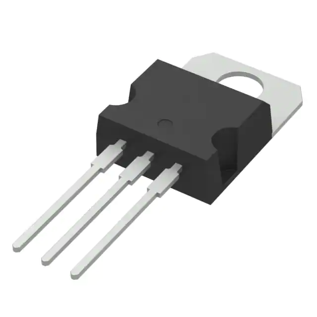
7. 封装信息:提供多种封装形式,如SOIC、DIP等。
STP80NF55L-06 价格&库存

很抱歉,暂时无法提供与“STP80NF55L-06”相匹配的价格&库存,您可以联系我们找货

免费人工找货
STP80NF55L-06

    库存:0

    STP80NF55L-06
    •  国内价格
    • 1+21.86540
    • 10+18.58560
    • 30+15.30580
    • 100+13.66590
    • 500+12.57260
    • 1000+10.93270

    库存:0