®
STPS30170C
HIGH VOLTAGE POWER SCHOTTKY RECTIFIER
Table 1: Main Product Characteristics IF(AV) VRRM Tj VF(max) 2 x 15 A 170 V 175 °C 0.75 V
A2 A2 A1 K K A1
A1 K A2
FEATURES AND BENEFITS
■ ■ ■
High junction temperature capability Low leakage current Good trade off between leakage current and forward voltage drop Insulated package: TO-220FPAB Insulating voltage: 2000 V DC Capacitance: 45 pF Avalanche specification
TO-247 STPS30170CW
TO-220AB STPS30170CT
■
K
■
A2 K A1 A1
A2
DESCRIPTION Dual center tab Schottky rectifier suited for High Frequency Switch Mode Power Supply.
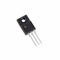
TO-220FPAB STPS30170CFP
D2PAK STPS30170CG
Table 2: Order Codes Part Numbers STPS30170CW STPS30170CT STPS30170CFP STPS30170CG STPS30170CG-TR Marking STPS30170CW STPS30170CT STPS30170CFP STPS30170CG STPS30170CG
September 2005
REV. 1
1/9
�STPS30170C
Table 3: Absolute Ratings (limiting values, per diode) Symbol VRRM IF(RMS) RMS forward current TO-220FPAB IF(AV) Average forward current TO-220AB / δ = 0.5 D2PAK TO-247 IFSM PARM Tstg Tj dV/dt Surge non repetitive forward current Repetitive peak avalanche power Storage temperature range Maximum operating junction temperature * Critical rate of rise of reverse voltage Tc = 120 °C Tc = 155 °C Per device tp = 10ms sinusoidal tp = 1µs Tj = 25 °C 30 220 10500 -65 to + 175 175 10000 A W °C °C V/µs Per diode 15 A Parameter Repetitive peak reverse voltage Value 170 30 Unit V A
1 dPtot * : --------------- > ------------------------- thermal runaway condition for a diode on its own heatsink Rth ( j – a ) dTj
Table 4: Thermal Parameters Symbol Parameter TO-220FPAB Rth(j-c) Junction to case TO-220AB / D2PAK TO-247 TO-220FPAB Rth(c) TO-220AB / TO-247
When the diodes 1 and 2 are used simultaneously: ∆ Tj(diode 1) = P(diode 1) x Rth(j-c)(Per diode) + P(diode 2) x Rth(c)
Value Per diode Total Per diode Total Per diode Total Coupling Coupling Coupling 4 3.3 1.6 0.85 1.5 0.8 2.6 0.3 0.3
Unit
°C/W
D2PAK
°C/W
Table 5: Static Electrical Characteristics (per diode) Symbol IR * Parameter Reverse leakage current Tests conditions Tj = 25 °C Tj = 125 °C Tj = 25 °C VF ** Forward voltage drop Tj = 125 °C Tj = 25 °C Tj = 125 °C
Pulse test: * tp = 5 ms, δ < 2% ** tp = 380 µs, δ < 2%
Min.
Typ 5
Max. 20 20 0.92
Unit µA mA
VR = VRRM IF = 15 A IF = 30 A
0.69
0.75 1
V
0.80
0.86
To evaluate the conduction losses use the following equation: P = 0.64 x IF(AV) + 0.0073 IF (RMS)
2
2/9
�STPS30170C
Figure 1: Average forward power dissipation versus average forward current (per diode)
PF(AV)(W)
14
d=0.1 d=0.2 d=0.5 d=1
Figure 2: Average forward current versus ambient temperature (δ = 0.5, per diode)
IF(AV)(A)
18 16 14 12 10 8 6
Rth(j-A)=15 °C/W Rth(j-a)=Rth(j-c) (TO-220FPAB) Rth(j-a)=Rth(j-c) (TO-220AB, TO -247 & D²PAK)
12 10 8 6 4
d=0.05
T
2 IF(AV)(A) 0 0 1 2 3 4 5 6 7 8 9 10 11 12 13 14 15 16 17 18
4
d=tp/T
tp
T
2 0 0
d=tp/T
25
tp
Tamb (°C) 50 75 100 125 150 175
Figure 3: Normalized avalanche derating versus pulse duration
PARM (t p ) PARM (1µs)
1
power
Figure 4: Normalized avalanche derating versus junction temperature
PARM (t p ) PARM (25°C)
power
1.2 1
0.1
0.8 0.6
0.01
0.4 0.2
0.001
0.01 0.1 1
t p (µs)
10 100 1000
Tj (°C)
0 25 50 75 100 125 150
Figure 5: Non repetitive surge peak forward current versus overload duration (maximum values, per diode) (TO-220AB, TO-247, D2PAK)
IM(A)
225
TO-220AB, TO -247 & D²PAK
Figure 6: Non repetitive surge peak forward current versus overload duration (maximum values, per diode) (TO-220FPAB)
IM(A)
140 130 120 110 100 90
TO-220FPAB
200 175 150 125 100
TC=75°C TC=50°C
80 70 60 50 40 30 20 10 0 1.E-03
TC=50°C
75 50
IM
TC=75°C
TC=125°C
IM t
TC=125°C
25 0 1.E-03
t
d =0.5
t(s) 1.E-02 1.E-01 1.E+00
d =0.5
t(s)
1.E-02
1.E-01
1.E+00
3/9
�STPS30170C
Figure 7: Relative variation of thermal impedance junction to case versus pulse duration (per diode) (TO-220AB, TO-247, D2PAK)
Zth(j-c)/Rth(j-c)
1.0
TO-220AB, TO -247 & D²PAK
Figure 8: Relative variation of thermal impedance junction to case versus pulse duration (per diode) (TO-220FPAB)
Zth(j-c)/Rth(j-c)
1.0
TO-220FPAB
0.9 0.8 0.7
d=0.5
0.9 0.8 0.7 0.6 0.5
d=0.5
0.6 0.5 0.4 0.3 0.2 0.1 0.0 1.E-03 1.E-02 1.E-01 1.E+00
Single pulse d=0.2 d=0.1
0.4 0.3
T
d=0.2 D=0.1
T
0.2
tP(s)
d=tp/T
tp
0.1
Single pulse
tP(s) 1.E-02 1.E-01
d =tp/T
1.E+00
tp
0.0 1.E-03 1.E+01
Figure 9: Reverse leakage current versus reverse voltage applied (typical values, per diode)
IR(µA)
1.E+06 1.E+05 1.E+04 1.E+03 1.E+02 1.E+01
Tj=25°C
Figure 10: Junction capacitance versus reverse voltage applied (typical values, per diode)
C(pF)
1000
F=1MHz VOSC=30mVRMS Tj=25°C
Tj=175°C
Tj=150°C Tj=125°C
100
Tj=75°C
1.E+00 1.E-01 0 VR(V) 10 20 30 40 50 60 70 80 90 100 110 120 130 140 150 160 170
10 1 10
VR(V) 100 1000
Figure 11: Forward voltage drop versus forward current (maximum values, per diode, low level)
IFM(A)
15.0
Figure 12: Forward voltage drop versus forward current (maximum values, per diode, high level)
IFM(A)
100
12.5
Tj=125°C (Maximum values)
Tj=125°C (Maximum values)
10.0
Tj=125°C (Typical values)
7.5
Tj=125°C (Typical values)
10
Tj=25°C (Maximum values)
5.0
Tj=25°C (Maximum values)
2.5
VFM(V)
VFM(V) 1
0.0 0.0 0.1 0.2 0.3 0.4 0.5 0.6 0.7 0.8 0.9 1.0
0.0
0.2
0.4
0.6
0.8
1.0
1.2
1.4
1.6
4/9
�STPS30170C
Figure 13: Thermal resistance junction to ambient versus copper surface under tab (Epoxy printed circuit board, copper thickness: 35 µm) (D2PAK)
Rth(j-a) (°C/W)
80
D²PAK
70 60 50 40 30 20 10 0 0 5 10 15 20 25 30 35 40 SCU(cm²)
Figure 14: TO-247 Package Mechanical Data DIMENSIONS REF.
V
Millimeters Min. Typ. Max. Min. 4.85 2.20 0.40 1.00 3.00 2.00 2.00 3.00 10.90 15.45 19.85 3.70 18.50 14.20 34.60 5.50 2.00 5° 60° 3.55 3.65 0.139 3.00 0.078 14.80 0.559 15.75 0.608 20.15 0.781 4.30 0.145 2.40 0.078 3.40 0.118 5.15 0.191 2.60 0.086 0.80 0.015 1.40 0.039
Inches Typ. Max. 0.203 0.102 0.031 0.055 0.118 0.078 0.094 0.133 0.429 0.620 0.793 0.169 0.728 0.582 1.362 0.216 0.118 5° 60° 0.143
A D E F F1
H A
V
Dia
F2 F3 F4 G H
L5 L L2 L4 F1 V2 F(x3) M G E F2 F3 F4 L3 D L1
L L1 L2 L3 L4 L5 M V V2 Dia.
5/9
�STPS30170C
Figure 15: D2PAK Package Mechanical Data DIMENSIONS Millimeters Inches Min. Max. Min. Max. 4.40 4.60 0.173 0.181 2.49 2.69 0.098 0.106 0.03 0.23 0.001 0.009 0.70 0.93 0.027 0.037 1.14 1.70 0.045 0.067 0.45 0.60 0.017 0.024 1.23 1.36 0.048 0.054 8.95 9.35 0.352 0.368 10.00 10.40 0.393 0.409 4.88 5.28 0.192 0.208 15.00 15.85 0.590 0.624 1.27 1.40 0.050 0.055 1.40 1.75 0.055 0.069 2.40 3.20 0.094 0.126 0.40 typ. 0.016 typ. 0° 8° 0° 8°
REF.
A E L2 C2
D L L3 A1 B2 B G A2 R
C
M
*
V2
* FLAT ZONE NO LESS THAN 2mm
A A1 A2 B B2 C C2 D E G L L2 L3 M R V2
Figure 16: Foot Print Dimensions (in millimeters)
16.90
10.30 1.30
5.08
3.70 8.90
6/9
�STPS30170C
Figure 17: TO-220FPAB Package Mechanical Data REF.
A H B
Dia L6 L2 L3 L5 F1 L4 F2 D L7
F G1 G
E
A B D E F F1 F2 G G1 H L2 L3 L4 L5 L6 L7 Dia.
DIMENSIONS Millimeters Inches Min. Max. Min. Max. 4.4 4.6 0.173 0.181 2.5 2.7 0.098 0.106 2.5 2.75 0.098 0.108 0.45 0.70 0.018 0.027 0.75 1 0.030 0.039 1.15 1.70 0.045 0.067 1.15 1.70 0.045 0.067 4.95 5.20 0.195 0.205 2.4 2.7 0.094 0.106 10 10.4 0.393 0.409 16 Typ. 0.63 Typ. 28.6 30.6 1.126 1.205 9.8 10.6 0.386 0.417 2.9 3.6 0.114 0.142 15.9 16.4 0.626 0.646 9.00 9.30 0.354 0.366 3.00 3.20 0.118 0.126
Figure 18: TO-220AB Package Mechanical Data REF. A C D E F F1 F2 G G1 H2 L2 L4 L5 L6 L7 L9 M Diam. DIMENSIONS Millimeters Inches Min. Max. Min. Max. 4.40 4.60 0.173 0.181 1.23 1.32 0.048 0.051 2.40 2.72 0.094 0.107 0.49 0.70 0.019 0.027 0.61 0.88 0.024 0.034 1.14 1.70 0.044 0.066 1.14 1.70 0.044 0.066 4.95 5.15 0.194 0.202 2.40 2.70 0.094 0.106 10 10.40 0.393 0.409 16.4 typ. 0.645 typ. 13 14 0.511 0.551 2.65 2.95 0.104 0.116 15.25 15.75 0.600 0.620 6.20 6.60 0.244 0.259 3.50 3.93 0.137 0.154 2.6 typ. 0.102 typ. 3.75 3.85 0.147 0.151
7/9
H2 Dia L5 C
A
L7 L6 L2 F2 F1 L9 L4 F G1 G M E D
�STPS30170C
In order to meet environmental requirements, ST offers these devices in ECOPACK® packages. These packages have a Lead-free second level interconnect . The category of second level interconnect is marked on the package and on the inner box label, in compliance with JEDEC Standard JESD97. The maximum ratings related to soldering conditions are also marked on the inner box label. ECOPACK is an ST trademark. ECOPACK specifications are available at: www.st.com. Table 6: Ordering Information Ordering type STPS30170CW STPS30170CT STPS30170CFP STPS30170CG STPS30170CG-TR
■ ■ ■ ■
Marking STPS30170CW STPS30170CT STPS30170CFP STPS30170CG STPS30170CG
Package TO-247 TO-220AB TO-220FPAB D2PAK
Weight 4.40 g 2g 1.9 g 1.48 g
Base qty 30 50 50 50 1000
Delivery mode Tube Tube Tube Tube Tape & reel
Epoxy meets UL94, V0 Cooling method: by conduction (C) TO-220 - Recommended torque value: 0.55 Nm, Maximum torque value: 0.7 Nm. TO-247 - Recommended torque value: 0.8 Nm, Maximum torque value: 1.0 Nm.
Table 7: Revision History Date 16-Sep-2005 Revision 1 First issue. Description of Changes
8/9
�STPS30170C
Information furnished is believed to be accurate and reliable. However, STMicroelectronics assumes no responsibility for the consequences of use of such information nor for any infringement of patents or other rights of third parties which may result from its use. No license is granted by implication or otherwise under any patent or patent rights of STMicroelectronics. Specifications mentioned in this publication are subject to change without notice. This publication supersedes and replaces all information previously supplied. STMicroelectronics products are not authorized for use as critical components in life support devices or systems without express written approval of STMicroelectronics. The ST logo is a registered trademark of STMicroelectronics. All other names are the property of their respective owners © 2005 STMicroelectronics - All rights reserved STMicroelectronics group of companies Australia - Belgium - Brazil - Canada - China - Czech Republic - Finland - France - Germany - Hong Kong - India - Israel - Italy - Japan Malaysia - Malta - Morocco - Singapore - Spain - Sweden - Switzerland - United Kingdom - United States of America www.st.com
9/9
�
很抱歉,暂时无法提供与“STPS30170CFP”相匹配的价格&库存,您可以联系我们找货
免费人工找货