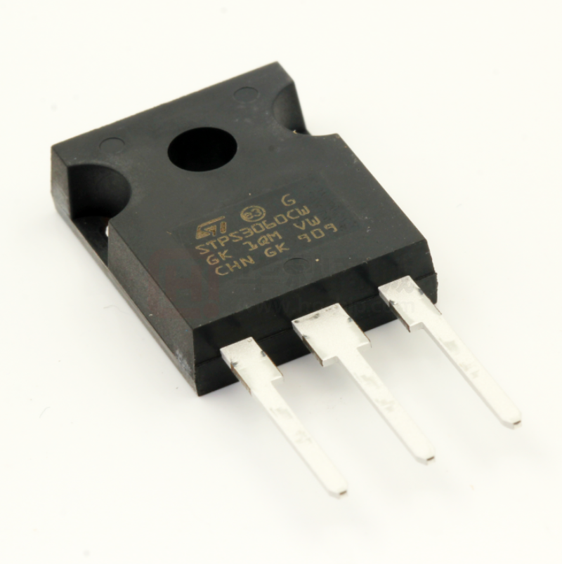
STPS3060CW
®
HIGH VOLTAGE POWER SCHOTTKY RECTIFIER
MAIN PRODUCT CHARACTERISTICS
IF(AV)
A1
2 x 15 A
K
A2
VRRM
60 V
Tj (max)
150°C
VF (max)
0.75 V
FEATURES AND BENEFITS
Negligible switching losses
Low forward voltage drop
Low capacitance
High reverse avalanche surge capability.
A2
■
K
■
A1
■
TO-247
STPS3060CW
■
DESCRIPTION
High voltage dual Schottky rectifier suited for
switchmode power supplies and other power
converters.
Packaged in TO-247, this device is intended for
use in medium voltage operation, and particularly,
in high frequency circuitries where low switching
losses and low noise are required.
ABSOLUTE RATINGS (limiting values, per diode)
Symbol
Parameter
VRRM
Repetitive peak reverse voltage
IF(RMS)
RMS forward current
δ = 0.5
Value
Unit
60
V
Per diode
30
A
Tc = 130°C
Per diode
Per device
15
30
A
IF(AV)
Average forward current
IFSM
Surge non repetitive forward current
tp = 10 ms
Sinusoidal
Per diode
200
A
IRRM
Repetitive peak reverse current
tp=2 µs
F=1kHz
Per diode
1
A
IRSM
Non repetitive peak reverse current
tp = 100µs
Per diode
1
A
Tstg
Storage temperature range
- 65 to + 150
°C
Maximum operating junction temperature *
150
°C
Critical rate of rise of reverse voltage
1000
V/µs
Tj
dV/dt
* :
dPtot
1
thermal runaway condition for a diode on its own heatsink
<
dTj
Rth( j − a )
October 2003 - Ed: 1A
1/4
�STPS3060CW
THERMAL RESISTANCES
Symbol
Rth(j-c)
Parameter
Per diode
Total
Coupling
Junction to case
Rth(c)
Value
Unit
1.5
0.8
0.1
°C/W
°C/W
When the diodes 1 and 2 are used simultaneously :
∆ Tj(diode 1) = P(diode1) x Rth(j-c)(Per diode) + P(diode 2) x Rth(c)
STATIC ELECTRICAL CHARACTERISTICS (per diode)
Symbol
Parameter
IR *
Tests Conditions
Reverse leakage
current
VF *
Tj = 25°C
Min.
Typ.
VR = VRRM
Tj = 125°C
Forward voltage drop
Tj = 25°C
IF = 15 A
Tj = 125°C
IF = 15 A
Tj = 25°C
IF = 30 A
Tj = 125°C
IF = 30 A
0.65
Max.
Unit
150
µA
100
mA
0.85
V
0.75
1.05
0.80
0.90
Pulse test: * tp = 5ms, δ < 2%
**tp = 380µs, δ < 2%
To evaluate the maximum conduction losses use the following equation :
P = 0.6 x IF(AV) + 0.01 IF2(RMS)
Fig. 1: Conduction losses versus average current
(per diode).
Fig. 2: Average forward current versus ambient
temperature (δ=0.5, per diode).
PF(AV)(W)
IF(AV)(A)
16
δ = 0.1
δ = 0.2
δ = 0.05
14
17
16
15
14
13
12
11
10
9
8
7
6
5
4
3
2
1
0
δ = 0.5
12
δ=1
10
8
6
4
T
2
IF(AV)(A)
δ=tp/T
0
0
2/4
2
4
6
8
10
12
14
16
tp
18
20
Rth(j-a)=Rth(j-I)
Rth(j-a)=15°C/W
T
δ=tp/T
0
Tamb(°C)
tp
25
50
75
100
125
150
�STPS3060CW
Fig. 3: Non repetitive surge peak forward current
versus overload duration (maximum values, per
diode).
Fig. 4: Relative variation of thermal impedance
junction to case versus pulse duration.
IM(A)
Zth(j-c)/Rth(j-c)
160
1.0
140
0.9
0.8
120
0.7
δ = 0.5
100
0.6
TC=50°C
80
60
0.5
0.4
δ = 0.2
0.3
δ = 0.1
TC=75°C
40
TC=110°C
IM
20
T
0.2
Single pulse
t
0.1
t(s)
δ=0.5
δ=tp/T
tp(s)
tp
0.0
0
1.E-03
1.E-02
1.E-01
1.E+00
Fig. 5: Reverse leakage currrent versus reverse
voltage applied (typical values, per diode).
1.E-03
1.E-02
1.E-01
1.E+00
Fig. 6: Junction capacitance versus reverse
voltage applied (typical values, per diode).
IR(mA)
C(pF)
1.E+01
10000
F=1MHz
VOSC=30mVRMS
Tj=25°C
Tj=125°C
1.E+00
Tj=100°C
Tj=75°C
1.E-01
1000
Tj=50°C
1.E-02
VR(V)
VR(V)
100
1.E-03
5
10
15
20
25
30
35
40
45
50
55
60
1
10
100
Fig. 7: Forward voltage drop versus forward
current (maximum values, per diode).
IFM(A)
1000
Tj=125°C
100
10
VFM(V)
1
0.0
0.2
0.4
0.6
0.8
1.0
1.2
1.4
1.6
1.8
3/4
�STPS3060CW
PACKAGE MECHANICAL DATA
TO-247
DIMENSIONS
REF.
V
A
H
L5
L
L2 L4
F2
F1
L1
F3
V2
F4
D
L3
F(x3)
M
G
=
■
■
■
■
Inches
Min. Typ. Max. Min.
A
4.85
5.15 0.191
D
2.20
2.60 0.086
E
0.40
0.80 0.015
F
1.00
1.40 0.039
F1
3.00
F2
2.00
F3 2.00
2.40 0.078
F4 3.00
3.40 0.118
G
10.90
H 15.45
15.75 0.608
L 19.85
20.15 0.781
L1 3.70
4.30 0.145
L2
18.50
L3 14.20
14.80 0.559
L4
34.60
L5
5.50
M
2.00
3.00 0.078
V
5°
V2
60°
Dia. 3.55
3.65 0.139
Dia.
V
Millimeters
E
=
Typ. Max.
0.203
0.102
0.031
0.055
0.118
0.078
0.094
0.133
0.429
0.620
0.793
0.169
0.728
0.582
1.362
0.216
0.118
5°
60°
0.143
Cooling method : C
Recommended torque value : 0.8m.N
Maximum torque value : 1.0m.N
Ordering type
Marking
Package
Weight
Base qty
Delivery
mode
STPS3060CW
STPS3060CW
TO-247
4.4 g
50
Tube
Epoxy meets UL94,V0
Information furnished is believed to be accurate and reliable. However, STMicroelectronics assumes no responsibility for the consequences of
use of such information nor for any infringement of patents or other rights of third parties which may result from its use. No license is granted by
implication or otherwise under any patent or patent rights of STMicroelectronics. Specifications mentioned in this publication are subject to
change without notice. This publication supersedes and replaces all information previously supplied. STMicroelectronics products are not authorized for use as critical components in life support devices or systems without express written approval of STMicroelectronics.
The ST logo is a registered trademark of STMicroelectronics.
All other names are the property of their respective owners.
© 2003 STMicroelectronics - All rights reserved.
STMicroelectronics GROUP OF COMPANIES
Australia - Belgium - Brazil - Canada - China - Czech Republic - Finland - France - Germany Hong Kong - India - Israel - Italy - Japan - Malaysia - Malta - Morocco - Singapore - Spain Sweden - Switzerland - United Kingdom - United States
www.st.com
4/4
�
很抱歉,暂时无法提供与“STPS3060CW”相匹配的价格&库存,您可以联系我们找货
免费人工找货- 国内价格
- 30+10.31491
- 150+10.10976