STPSC20H065C
650 V power Schottky silicon carbide diode
Datasheet - production data
Description
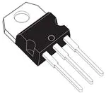
A1 (1)
K (2)
A2 (3)
A2
A1
K
TO-220AB
STPSC20H065CT
The SiC diode is an ultrahigh performance power
Schottky diode. It is manufactured using a silicon
carbide substrate. The wide band gap material
allows the design of a Schottky diode structure
with a 650 V rating. Due to the Schottky
construction, no recovery is shown at turn-off and
ringing patterns are negligible. The minimal
capacitive turn-off behavior is independent of
temperature.
Especially suited for use in PFC applications, this
ST SiC diode will boost the performance in hard
switching conditions. Its high forward surge
capability ensures a good robustness during
transient phases.
A2
K
Table 1. Device summary
A1
TO-247
STPSC20H065CW
Features
Symbol
Value
IF(AV)
2 x 10 A
VRRM
650 V
Tj (max)
175 °C
No or negligible reverse recovery
Switching behavior independent of
temperature
Dedicated to PFC applications
High forward surge capability
November 2013
This is information on a product in full production.
DocID023605 Rev 3
1/9
www.st.com
�Characteristics
1
STPSC20H065C
Characteristics
Table 2. Absolute ratings (limiting values per diode at 25 °C unless otherwise
specified)
Symbol
Parameter
VRRM
Repetitive peak reverse voltage
IF(RMS)
Forward rms current
Value
Unit
650
V
22
A
(1)
Tc = 135 °C , DC, per diode
10
Tc = 125 °C(2), per device
20
IF(AV)
Average forward current
IFSM
Surge non repetitive forward
current
tp = 10 ms sinusoidal, Tc = 25 °C
tp = 10 ms sinusoidal, Tc = 125 °C
tp = 10 µs square, Tc = 25 °C
90
80
470
A
IFRM
Repetitive peak forward current
Tc = 135 °C(1), Tj = 175 °C, = 0.1
36
A
Tstg
Storage temperature range
-55 to +175
°C
-40 to +175
°C
Operating junction
Tj
temperature(3)
A
1. Value based on Rth(j-c) max (per diode)
2. Value based on Rth(j-c) max (per device)
3.
dPtot
--------------dTj
1
- condition to avoid thermal runaway for a diode on its own heatsink
------------------------Rth j – a
Table 3. Thermal resistance
Value
Symbol
Parameter
Unit
TO-247
Per diode
Rth(j-c)
TO-220AB
Junction to case per diode
TO-247
Total
Rth(c)
TO-220AB
Typ.
Max.
1.25
1.5
0.83
0.95
Coupling
°C/W
0.4
When the two diodes 1 and 2 are used simultaneously:
Tj(diode 1) = P(diode 1) x Rth(j-c)(Per diode) + P(diode 2) x Rth(c)
Table 4. Static electrical characteristics per diode
Symbol
Parameter
Tests conditions
IR (1)
Reverse leakage current
VF (2)
Forward voltage drop
Tj = 25 °C
Tj = 150 °C
Tj = 25 °C
Tj = 150 °C
Min.
Typ.
Max.
-
9
100
-
85
425
-
1.56
1.75
-
1.98
2.5
VR = VRRM
IF = 10 A
1. tp = 10 ms, < 2%
2. tp = 500 µs, < 2%
To evaluate the conduction losses use the following equation:
P = 1.35 x IF(AV) + 0.115 x IF2(RMS)
2/9
DocID023605 Rev 3
Unit
µA
V
�STPSC20H065C
Characteristics
Table 5. Dynamic electrical characteristics per diode
Symbol
Parameter
Qcj(1)
Test conditions
Total capacitive charge
Cj
Total capacitance
Typ.
Unit
VR = 400 V
28.5
nC
VR = 0 V, Tc = 25 °C, F = 1 MHz
480
VR = 400 V, Tc = 25 °C, F = 1 MHz
48
1. Most accurate value for the capacitive charge:
pF
VOUT
Qcj =
∫0 cj(vR).dvR
Figure 1. Forward voltage drop versus forward Figure 2. Forward voltage drop versus forward
current (typical values per diode, low level)
current (typical values per diode, high level)
20
IFM(A)
18
IFM(A)
100
Pulse test : tp=500µs
16
80
Ta=25 °C
14
12
Pulse test : tp=500µs
90
70
Ta=150 °C
Ta=100 °C
10
60
8
40
6
30
4
20
2
Ta=25 °C
50
Ta=175 °C
Ta=100 °C
Ta=150 °C
10
VFM(V)
0
Ta=175 °C
VFM(V)
0
0.0
0.5
1.0
1.5
2.0
2.5
3.0
3.5
Figure 3. Reverse leakage current versus
reverse voltage applied (typical values per
diode)
1.E+03
IR(µA)
0
1
2
3
4
5
6
I M (A)
T
δ = 0.1
70
Tj=175 °C
δ=tp/T
60
tp
50
Tj=150 °C
1.E+01
8
Figure 4. Peak forward current versus case
temperature, per diode
80
1.E+02
7
δ = 0.3
40
1.E+00
δ = 0.5
30
20
1.E-01
Tj=25 °C
δ=1
VR(V)
1.E-02
δ = 0.7
10
TC(°C)
0
0
50
100 150 200 250 300 350 400 450 500 550 600 650
0
DocID023605 Rev 3
25
50
75
100
125
150
175
3/9
9
�Characteristics
STPSC20H065C
Figure 5. Junction capacitance versus reverse
voltage applied (typical values, per diode)
500
Cj (pF)
Figure 6. Relative variation of thermal
impedance junction to case versus pulse
duration per diode
Zth(j-c)/Rth(j-c)
1.0
F=1 MHz
VOSC=30 mVRMS
Tj=25 °C
450
400
0.9
0.8
350
0.7
300
0.6
250
0.5
200
0.4
150
0.3
100
0.2
50
0.1
10.0
0.0
1.E-05
0
0.1
1.0
100.0
1000.0
Figure 7. Non-repetitive peak surge forward
current versus pulse duration per diode
(sinusoidal waveform)
1.E+03
Single pulse
VR(V)
IFSM (A)
tp(s)
1.E-04
1.E-03
1.E-02
1.E-01
1.E+00
Figure 8. Total capacitive charges versus
reverse voltage applied (typical values per
diode)
32
Qcj (nC)
28
Ta=25 °C
24
20
Ta=125 °C
16
1.E+02
12
8
4
VR (V)
tp(s)
1.E+01
1.E-05
4/9
0
1.E-04
1.E-03
1.E-02
0
DocID023605 Rev 3
50
100
150
200
250
300
350
400
�STPSC20H065C
2
Package information
Package information
Epoxy meets UL94, V0
Cooling method: conduction (C)
Recommended torque value:
–
TO-220AB 0.4 to 0.6 N·m,
–
TO-247 0.55 N·m (1.0 N·m maximum)
In order to meet environmental requirements, ST offers these devices in different grades of
ECOPACK® packages, depending on their level of environmental compliance. ECOPACK®
specifications, grade definitions and product status are available at: www.st.com.
ECOPACK® is an ST trademark.
Figure 9. TO-220AB dimension definitions
A
H2
Dia
C
L5
L7
L6
L2
F2
F1
D
L9
L4
F
M
G1
E
G
DocID023605 Rev 3
5/9
9
�Package information
STPSC20H065C
Table 6. TO-220AB dimension values
Dimensions
Ref.
Millimeters
Min.
Max.
Min.
Max.
A
4.40
4.60
0.173
0.181
C
1.23
1.32
0.048
0.051
D
2.40
2.72
0.094
0.107
E
0.49
0.70
0.019
0.027
F
0.61
0.88
0.024
0.034
F1
1.14
1.70
0.044
0.066
F2
1.14
1.70
0.044
0.066
G
4.95
5.15
0.194
0.202
G1
2.40
2.70
0.094
0.106
H2
10
10.40
0.393
0.409
L2
16.4 typ.
0.645 typ.
L4
13
14
0.511
0.551
L5
2.65
2.95
0.104
0.116
L6
15.25
15.75
0.600
0.620
L7
6.20
6.60
0.244
0.259
L9
3.50
3.93
0.137
0.154
M
Diam.
6/9
Inches
2.6 typ.
3.75
0.102 typ.
3.85
DocID023605 Rev 3
0.147
0.151
�STPSC20H065C
Package information
Figure 10. TO-247 dimension definitions
Heat-sink plane
A
E
∅P
S
∅R
D
L2
L1
b1
L
b2
1
2
3
b
c
3
2
1
BACK VIEW
A1
e
Table 7. TO-247 dimension values
Dimensions
Ref.
Millimeters
Min.
Typ.
Inches
Max.
Min.
Typ
Max.
A
4.85
5.15
0.191
0.203
A1
2.20
2.60
0.086
0.102
b
1.00
1.40
0.039
0.055
b1
2.00
2.40
0.078
0.094
b2
3.00
3.40
0.118
0.133
c
0.40
0.80
0.015
0.031
D(1)
19.85
20.15
0.781
0.793
E
15.45
15.75
0.608
0.620
e
5.30
5.60
0.209
L
14.20
14.80
0.559
0.582
L1
3.70
4.30
0.145
0.169
L2
P
(2)
5.45
18.50 typ.
0.215
0.220
0.728 typ.
3.55
3.65
0.139
0.143
R
4.50
5.50
0.177
0.217
S
5.30
5.70
0.209
5.50
0.216
0.224
1. Dimension D plus gate protrusion does not exceed 20.5 mm
2. Resin thickness around the mounting hole is not less than 0.9 mm
DocID023605 Rev 3
7/9
9
�Ordering information
3
STPSC20H065C
Ordering information
Table 8. Ordering information
4
Order code
Marking
Package
Weight
Base qty
Delivery mode
STPSC20H065CT
STPSC20H065C
TO-220AB
1.86 g
50
Tube
STPSC20H065CW
STPSC20H065CW
TO-247
4.43 g
30
Tube
Revision history
Table 9. Document revision history
8/9
Date
Revision
Changes
31-Aug-2012
1
First issue.
10-Oct-2012
2
Added Max. values to Table 3.
07-Nov-2013
3
Updated Figure 1 and Figure 2.
DocID023605 Rev 3
�STPSC20H065C
Please Read Carefully:
Information in this document is provided solely in connection with ST products. STMicroelectronics NV and its subsidiaries (“ST”) reserve the
right to make changes, corrections, modifications or improvements, to this document, and the products and services described herein at any
time, without notice.
All ST products are sold pursuant to ST’s terms and conditions of sale.
Purchasers are solely responsible for the choice, selection and use of the ST products and services described herein, and ST assumes no
liability whatsoever relating to the choice, selection or use of the ST products and services described herein.
No license, express or implied, by estoppel or otherwise, to any intellectual property rights is granted under this document. If any part of this
document refers to any third party products or services it shall not be deemed a license grant by ST for the use of such third party products
or services, or any intellectual property contained therein or considered as a warranty covering the use in any manner whatsoever of such
third party products or services or any intellectual property contained therein.
UNLESS OTHERWISE SET FORTH IN ST’S TERMS AND CONDITIONS OF SALE ST DISCLAIMS ANY EXPRESS OR IMPLIED
WARRANTY WITH RESPECT TO THE USE AND/OR SALE OF ST PRODUCTS INCLUDING WITHOUT LIMITATION IMPLIED
WARRANTIES OF MERCHANTABILITY, FITNESS FOR A PARTICULAR PURPOSE (AND THEIR EQUIVALENTS UNDER THE LAWS
OF ANY JURISDICTION), OR INFRINGEMENT OF ANY PATENT, COPYRIGHT OR OTHER INTELLECTUAL PROPERTY RIGHT.
ST PRODUCTS ARE NOT DESIGNED OR AUTHORIZED FOR USE IN: (A) SAFETY CRITICAL APPLICATIONS SUCH AS LIFE
SUPPORTING, ACTIVE IMPLANTED DEVICES OR SYSTEMS WITH PRODUCT FUNCTIONAL SAFETY REQUIREMENTS; (B)
AERONAUTIC APPLICATIONS; (C) AUTOMOTIVE APPLICATIONS OR ENVIRONMENTS, AND/OR (D) AEROSPACE APPLICATIONS
OR ENVIRONMENTS. WHERE ST PRODUCTS ARE NOT DESIGNED FOR SUCH USE, THE PURCHASER SHALL USE PRODUCTS AT
PURCHASER’S SOLE RISK, EVEN IF ST HAS BEEN INFORMED IN WRITING OF SUCH USAGE, UNLESS A PRODUCT IS
EXPRESSLY DESIGNATED BY ST AS BEING INTENDED FOR “AUTOMOTIVE, AUTOMOTIVE SAFETY OR MEDICAL” INDUSTRY
DOMAINS ACCORDING TO ST PRODUCT DESIGN SPECIFICATIONS. PRODUCTS FORMALLY ESCC, QML OR JAN QUALIFIED ARE
DEEMED SUITABLE FOR USE IN AEROSPACE BY THE CORRESPONDING GOVERNMENTAL AGENCY.
Resale of ST products with provisions different from the statements and/or technical features set forth in this document shall immediately void
any warranty granted by ST for the ST product or service described herein and shall not create or extend in any manner whatsoever, any
liability of ST.
ST and the ST logo are trademarks or registered trademarks of ST in various countries.
Information in this document supersedes and replaces all information previously supplied.
The ST logo is a registered trademark of STMicroelectronics. All other names are the property of their respective owners.
© 2013 STMicroelectronics - All rights reserved
STMicroelectronics group of companies
Australia - Belgium - Brazil - Canada - China - Czech Republic - Finland - France - Germany - Hong Kong - India - Israel - Italy - Japan Malaysia - Malta - Morocco - Philippines - Singapore - Spain - Sweden - Switzerland - United Kingdom - United States of America
www.st.com
DocID023605 Rev 3
9/9
9
�