STR485
Datasheet
3.3 V RS485 compatible with 1.8 V I/Os and selectable speed
20 Mbps or 250 kbps
Features
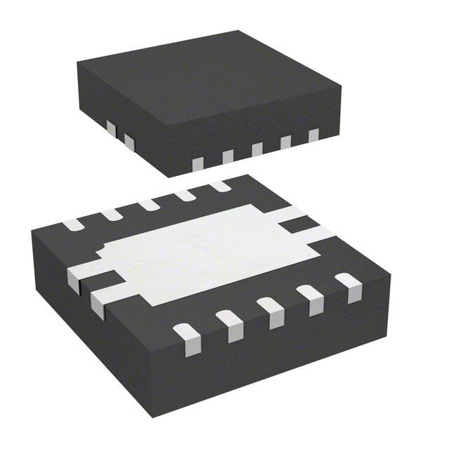
DFN10 3 x 3
•
•
•
•
•
•
•
•
•
•
•
•
Half-duplex RS485 transceiver
1.65 V to 3.6 V supply for data and enable signals
3 V to 3.6 V supply for bus supply
High speed: up to 20 Mbps data rate
Low speed selected by SLR pin : 250 kbps
Up to 256 transceivers on the bus
Fail safe receiver (bus open, idle and shorted)
Thermal shutdown protection
Low quiescent current in shutdown mode
Extended temperature range : -40 °C to +105 °C
Available in industry standard DFN10
Bus-pin protection more than:
–
±4 kV HBM protection
–
±8 kV IEC61000-4-2 contact discharge
–
±16 kV IEC61000-4-2 air discharge
–
Compliant IEC61000-4-4 fast transient burst Class B
Description
Product status link
STR485
The STR485 is a low power differential line transceiver for data transmission
standard RS485 applications in half-duplex mode. Data and enable signals are
compatible with 1.8 V or 3.3 V supplies.
Two speeds are selectable through SLR pin: fast data rate up to 20 Mbps or slow
data rate for extended cable running to 250 kbps.
Excessive power dissipation caused by bus contention or faults is prevented by
thermal shutdown circuit that forces the driver outputs into a high impedance state.
The receiver has a fail-safe feature, which guarantees a high output state when the
inputs are left open, shorted or idle.
DS12713 - Rev 5 - July 2020
For further information contact your local STMicroelectronics sales office.
www.st.com
�STR485
Pin connections
1
Pin connections
Figure 1. Pin connections
VL
VCC
R
B
DE
A
RE
SLR
D
GND
Table 1. Pin description
DS12713 - Rev 5
Name
Pin
I/O
Description
VL
1
Logic supply
1.65 V to 3.6 V supply for logic I/O signals
R
2
Digital output
Receiver data output
DE
3
Digital input
nRE
4
Digital input
D
5
Digital input
GND
6
Ground
SLR
7
Digital input
A
8
Bus I/O
Digital bus I/O, A
B
9
Bus I/O
Digital bus I/O, B
VCC
10
Bus supply
3 V to 3.6 V supply for A and B bus lines
Driver enable input:
serial resistors of 150 ohms followed by 2.5 Mohms/GND
Receiver enable input:
serial resistors of 150 ohms followed by 2.5 Mohms/VCC
Transmission data input
Slew rate select: low = 20 Mbps, high = 250 kbps.
Default to 20 Mbps if SLR is left floating
page 2/26
�STR485
Pin connections
Figure 2. Typical application schematic
1.8 V
VL
SLR
3.3 V
3.3 V
VCC
A
VCC
SLR
RT
120 Ω
D
B
DE
VL
A
RT
120 Ω
D
1.8 V
DE
B
R
R
RE
RE
GND
GND
Figure 3. Example of implementation in a PCB
Adding an ESDA14V2BP6 or ETP01-2821 STMicroelectronics protection device can help the product to sustain
an EFT perturbation level up to 4 kV.
DS12713 - Rev 5
page 3/26
�STR485
Truth tables
2
Truth tables
The STR485 is a half-duplex differential driver/receiver compliant to the RS485 communication standard (ISO-IEC
8482). This product is perfectly adapted for low voltage application running with a low power supplies VL,
generally set to 1.8 V and VCC set to 3.3 V.
These voltages confer a low power consumption to the product.
SLR is the data rate selection, this pin could be let floating but it is not recommended; in that case the high speed
rate is automatically selected.
The SLR pin must be connected to the ground to provide a high speed communication up to 20 Mbps.
When this pin is connected to VL power supply, the data rate is limited to 250 kbps more adapted for very long
distance data transmission.
Figure 4. Block diagram
The product is perfectly adapted to run with 256 devices on the same bus thanks to the internal output resistance
that is over 96 kΩ up to 105 °C; this resistance follows the RS485 condition that requests a minimum of 12 kΩ for
32 unit loads (UL).
The STR485 has internal protection against ESD that protect each device driver output and receiver input. The
limits have been tested up ±4 kV electrostatic discharge (HBM) and ± 8 kV contact discharge and ± 16 kV air
discharge shocks without latch-up.
Another external protections can be used to increase the communication robustness against different perturbation
that can be seen on the application.
The power supplies must be well-decoupled by a minimal capacitor of 0.1 µF as closed as possible to the device
power supply input. Moreover, the capacitor should be higher on the application with a minimum of 1 µF around
the device.
The device operating range is set from VL = 1.65 V to 3.6 V and for Vcc = 3.0 V to 3.6 V. In any case VCC must
be higher or equal than VL.
The applications should respect this voltage constraints to let the application communication device run to the
best conditions.
DS12713 - Rev 5
page 4/26
�STR485
Truth tables
Figure 5. Example of typical application
VCC VL
SLR
SLR
A
DE
VCC
RT
120Ω
RT
120Ω
D
VL
A
D
B
DE
B
R
R
B
RE
GND
A
B
SLR
SLR
VL
VL
VCC
GND
D
DE
R
A
RE
GND
VCC
GND
D
RE
DE
R
RE
Table 2. Driver truth table
INPUT D
ENABLE DE
OUTPUT A
OUTPUT B
Function
H
H
H
L
Actively drive bus high
L
H
L
H
Actively drive bus low
X
L
Z
Z
Driver disabled
X
Open
Z
Z
Driver disabled by default
Open
H
H
L
Actively drive bus high by default
Table 3. Receiver truth table
Differential input VID = VA -VB
ENABLE RE
OUTPUT R
Function
VID > VIT+
L
H
Receive valid bus high
VIT- < VID < VIT+
L
?
Indeterminate bus state
VID < VIT-
L
L
Receive valid bus low
X
H
Z
Receiver disabled
X
OPEN
Z
Receiver disabled by default
Open-circuit bus
L
H
Fail safe high output
Short-circuit bus
L
H
Fail safe high output
Idle (terminated) bus
L
H
Fail safe high output
Table 4. Speed selection, SLR pin configuration
DS12713 - Rev 5
SLR
Data rate
Typical tr / tf
VL
250 kbps
200 ns
GND or OPEN
20 Mbps
7 ns
page 5/26
�STR485
Absolute maximum ratings and operating conditions
3
Absolute maximum ratings and operating conditions
Table 5. Absolute maximum ratings
Symbol
VL
VCC
Parameter
Min.
Max.
Unit
Control supply voltage
-0.5
4
V
Bus supply voltage
-0.5
4.8
V
Voltage range at A or B inputs
-13
13
V
Input voltage range at any logic pin
-0.3
VL+0.3
V
Receiver output current
-12
12
mA
170
°C
150
°C
IEC 61000-4-2 ESD (air-gap discharge), bus terminals and GND
± 16
kV
IEC 61000-4-2 ESD (contact discharge), bus terminals and GN
±8
kV
IEC 61000-4-4 EFT (fast transient or burst) bus terminals and GND
±2
kV
JEDEC standard 22, test method A114, HBM, all terminals
±4
kV
± 1.5
kV
TJ
Junction temperature
Tstg
Storage temperature
ESD
-65
JEDEC standard 22, test method C101, (charged device model), all pins
Note:
All voltage values, except the differential voltage, are with respect to network ground terminal.
Table 6. Operating conditions
Symbol
VL
VCC
Parameter
Control supply voltage
Min.
Typ.
1.65
Max.
Unit
3.6
Bus supply voltage
3
VI
Input level at any bus terminal (separately or common mode)
-7
12
VIH
High level input voltage (driver, driver enabled, receiver enable inputs, and slew rate
select)
0.7×VL
VL
VIL
Low level input voltage (driver, driver enable, receiver enable inputs, and slew rate
select)
0
0.3×VL
VID
Differential input voltage
-12
12
Output current / driver
-80
80
Output current / receiver
-2
2
RL
Differential load resistance
54
CL
Differential load capacitance
IO
DR
TA
3.3
3.6
V
mA
60
Ω
50
pF
Signaling rate / SLR = ‘0’
20
Mbps
Signaling rate / SLR = ‘1’
250
kbps
105
°C
Operating free-air temperature
-40
Operation is specified for internal (junction temperature) up to 150 °C. Self-heating due to internal power
dissipation should be considered for each application. Maximum junction temperature is internally limited by the
thermal shut-down circuit which disables the driver outputs when the junction temperature reaches 165 °C.
DS12713 - Rev 5
page 6/26
�STR485
Absolute maximum ratings and operating conditions
Table 7. Thermal information
DS12713 - Rev 5
Symbol
Parameter
Min.
Typ.
Rth-ja
Thermal resistance, junction-to-ambient
40
Rth-jc
Thermal resistance, junction-to-case
5.2
Max.
Unit
°C/W
page 7/26
�STR485
Electrical characteristics
4
Electrical characteristics
Table 8. Receiver: over recommended operating conditions (unless otherwise specified. Please, see
"Operating conditions" table)
Symbol
Parameter
Test conditions
Min.
Typ.
Max.
Unit
Receiver/DC
VIT+
Positive-going receiver
differential input voltage
threshold
(1)
-60
-20
VIT-
Negative-going receiver
differential input voltage
threshold
-200
-130
(1)
40
70
VL = 1.65 V, IOH = - 2 mA
1.25
1.45
VL = 3 V, IOH = - 2 mA
2.75
2.9
VHYS
Receiver differential input
voltage threshold
hysteresis (VIT+ - VIT- )(1)
VOH
Receiver high-level
output voltage
VOL
Receiver low-level output
voltage
COD
Differential output
capacitance
IOZ
Receiver output highimpedance current
Rin
Receiver input
impedance
VL = 1.65 V, IOL = 2 mA
0.2
0.45
VL = 3 V, IOL = 2 mA
0.1
0.25
15
VO = 0 V or VL, nRE at VL
-7 V ≤ Vincm ≤ +12 V
-40 °C ≤ Temp ≤ 105 °C
-1
II
1
µA
kΩ
85(2)
VI = 12 V, -40 °C ≤ Temp ≤ 105 °
VI = -7 V, -40 °C ≤ Temp ≤ 105 °
V
pF
96 (2)
1V65 < VL < 3.3 V, VCC = 3.3 V
Receiver input current
(disabled driver)
mV
125(2)
µA
-100(2)
Receiver / switching characteristics, SLR = ‘X’
tr, tf
Receiver output rise/fall
time
tPHL, tPLH
Receiver propagation
delay time
tSK(P)
Receiver pulse skew, |
tPHL – tPLH|
tPLZ, tPHZ
Receiver disable time
tPLZ, tPZH, tPZL,
tPZH
Receiver enable time
CL=15 pF
15
5
15
25
60
15
12
20
Driver enabled CL=15 pF with 1 kΩ
15
80
Driver disabled CL=15 pF with
1 kΩ
2
8
ns
µs
1. Under any specific conditions, VIT+, is specified to be at least VHYS higher than VIT2. Guaranteed by design simulation in temperature.
DS12713 - Rev 5
page 8/26
�STR485
Electrical characteristics
Table 9. Driver: over recommended operating conditions (unless otherwise specified. Please, see
"Operating conditions" table)
Symbol
Parameter
Test conditions
Min.
Typ.
Max.
Unit
2
µA
DC driver/ DC
II
|VOD|
Driver input, driver enable,
and receiver enable input
current
Driver differential output
voltage magnitude
Δ|VOD|
Change in magnitude of
driver differential output
voltage
V°C(SS)
Steady-state commonmode output voltage
ΔV°C
Change in differential
driver output commonmode voltage
V°C(PP)
Peak-to-peak driver
common-mode output
voltage
-2
RL = 60 Ω, 375 Ω on
each output to –7 V to
12
1.5
2
RL = 54 Ω (RS-485)
1.5
2
RL = 100 Ω (RS-422)
TJ ≥ 0 °C, VCC ≥ 3.2
2
RL = 54 Ω, CL = 50 pF
Center of two 27-Ω
load resistors
V
-50
0
50
mV
1
VCC/2
3
V
-50
0
50
mV
500
Driver/switching characteristics, SLR='1', 250 kbps, bit time ≥ 4 µs
tr, tf
Driver differential output
rise/fall time
tPHL, tPLH
Driver propagation delay
time
tSK(P)
Driver pulse skew, |tPHL –
tPLH|
tPLZ, tPHZ
tPLZ, tPZH
0.05
0.2
1
0.4
1
1.5
RL=54 Ω, CL=50 pF
0.3
Driver disable time
Driver enable time
0.017
0.035
Receiver enabled
CL=50 pF with 110 kΩ
0.7
1.2
Receiver disabled
CL=50 pF with 110 kΩ
1.64
2.4
µs
µs
Driver/switching characteristics, SLR= '0', 20 Mbps, bit time ≥ 50 ns
DS12713 - Rev 5
tr, tf
Driver differential output
rise/fall time
tPHL, tPLH
Driver propagation delay
tSK(P)
Driver pulse skew, |tPHL –
tPLH|
tPLZ, tPHZ
Driver disable time
tPZL, tPZH
Driver enable time
RL=54 Ω, CL=50 pF
4
7
15
6
12
25
4
17
40
Receiver enabled
9
18
Receiver disabled
1
2.4
ns
µs
page 9/26
�STR485
Electrical characteristics
Table 10. Supply current and protections: over recommended operating conditions (unless otherwise
specified. Please, see "Operating conditions" table)
Symbol
Parameter
Test conditions
Min.
Typ.
Max.
Unit
Supply current
Driver and receiver enabled
625
DE = VL, RE = GND, no load,
Tamb
µA
Driver and receiver enabled
900 (1)
DE = VL, RE = GND, no load,
T