STSMIA832
1.8 V / 2.8 V high speed dual differential line receivers,
standard mobile imaging architecture (SMIA) decoder deserializer
Features
■
Sub-low voltage differential signaling inputs:
VID = 100 mV min. with RT = 100 Ω, CL = 10 pF
■
High signaling rate:
fIN = 650 Mbps max (D+,D-,STRB+,STRB-)
fOUT = 82 MHz max (CLK)
fOUT = 82 Mbps max (for each data line D1-D8)
■
Very high speed strobe to clock:
tPLH ~ tPHL = 5.2 ns (typ) at VDD = 2.8 V;
VL = 1.8 V
■
Operating voltage range:
VDD(OPR) = 2.65 V to 3.6 V
VL(OPR) = 1.65 V to 1.95 V
Description
■
Symmetrical output impedance
(D1-D8, H-SYNC, V-SYNC, CLK):
IIOHI = IOL = 4 mA (min) at VDD = 2.65 V;
VL = 1.8 V
■
Low power dissipation (disabled: EN = gnd):
ISOFF = IDD + IL = 10 µA (Max)
■
SMIA specification compliant
■
Support for SMIA CCP RAW8, RAW10 and
RAW12 8-bit packet
■
CLASS 0 and CLASS 1, 2 supported (config.
by CLASS_SEL)
■
CMOS logic input threshold
(EN, SYNC_SEL, CLASS_SEL):
VIL = 0.3 x VL; VL = 1.65 V to 1.95 V
VIH = 0.7 x VL; VL = 1.65 V to 1.95 V
■
3.6 V tolerant on inputs
(EN, SYNC_SEL, CLASS_SEL)
■
32 BIT synchronization codes (SOF, EOF,
SOL, EOL)
■
Leadfree TFBGA package
(RoHS restriction of hazardous substances)
Applications
■
Feature phone (Mid-end 2 - 8 MPixel)
■
PDA, digital camera
■
Notebook, eBook (webcam), UMPC, MID
May 2010
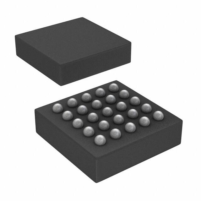
TFBGA25
The STSMIA832 receiver converts the subLVDS
clock/datastream (up to 650 Mbps throughput
bandwidth) back into parallel 8 bits of
CMOS/LVTTL. The device recognizes the SMIA
32 bit start of frame (SOF), end of frame (EOF),
start of line (SOL) and end of line (EOL)
sequences to generate the H-SYNC and V-SYNC
signals. Output LVTTL clock (up to 82 MHz) is
transmitted in parallel with data. Output data are
rising-edge strobes. This chipset is an ideal
means to link mobile camera modules to
Baseband processors. In order to minimize static
current consumption, it is possible to shut down
the device when the interface is not being used by
a power-down (EN) pin that reduces the
maximum current consumption to 10 µA making
this device ideal for portable applications like
mobile phone and portable battery equipment. A
configurable input (Class_Sel) is provided to
select different CLASS (0 or 1, 2) mode inside the
SMIA standard specifications.
The STSMIA832 is offered in a TFBGA package
to optimize PCB space. All inputs and outputs are
equipped with protection circuits against static
discharge, giving them ESD immunity from
transient excess voltage. The STSMIA832 is
characterized for operation over the commercial
temperature range - 40 °C to 85 °C.
Doc ID 12174 Rev 5
1/25
www.st.com
25
�Contents
STSMIA832
Contents
1
Schematic diagram . . . . . . . . . . . . . . . . . . . . . . . . . . . . . . . . . . . . . . . . . . 3
2
Pin configuration . . . . . . . . . . . . . . . . . . . . . . . . . . . . . . . . . . . . . . . . . . . . 4
3
2.1
Pin descriptions for reference: . . . . . . . . . . . . . . . . . . . . . . . . . . . . . . . . . . 5
2.2
Supplementary notes: SMIA specification . . . . . . . . . . . . . . . . . . . . . . . . . 6
Application information . . . . . . . . . . . . . . . . . . . . . . . . . . . . . . . . . . . . . . 9
3.1
Inputs . . . . . . . . . . . . . . . . . . . . . . . . . . . . . . . . . . . . . . . . . . . . . . . . . . . . . 9
3.2
Power down mode . . . . . . . . . . . . . . . . . . . . . . . . . . . . . . . . . . . . . . . . . . . 9
3.3
Power saving at the inputs . . . . . . . . . . . . . . . . . . . . . . . . . . . . . . . . . . . . 10
3.4
Switching off digital blocks . . . . . . . . . . . . . . . . . . . . . . . . . . . . . . . . . . . . 10
3.5
Disabling the outputs . . . . . . . . . . . . . . . . . . . . . . . . . . . . . . . . . . . . . . . . 10
3.6
Load capacitance . . . . . . . . . . . . . . . . . . . . . . . . . . . . . . . . . . . . . . . . . . . 10
3.7
Board layout . . . . . . . . . . . . . . . . . . . . . . . . . . . . . . . . . . . . . . . . . . . . . . . 11
3.8
Decoupling capacitors . . . . . . . . . . . . . . . . . . . . . . . . . . . . . . . . . . . . . . . 11
4
Maximum ratings . . . . . . . . . . . . . . . . . . . . . . . . . . . . . . . . . . . . . . . . . . . 13
5
Electrical characteristics . . . . . . . . . . . . . . . . . . . . . . . . . . . . . . . . . . . . 14
6
Frame structure . . . . . . . . . . . . . . . . . . . . . . . . . . . . . . . . . . . . . . . . . . . . 17
7
Timing diagram . . . . . . . . . . . . . . . . . . . . . . . . . . . . . . . . . . . . . . . . . . . . 18
8
Package mechanical data . . . . . . . . . . . . . . . . . . . . . . . . . . . . . . . . . . . . 20
9
Order code . . . . . . . . . . . . . . . . . . . . . . . . . . . . . . . . . . . . . . . . . . . . . . . . 23
10
Revision history . . . . . . . . . . . . . . . . . . . . . . . . . . . . . . . . . . . . . . . . . . . 24
2/25
Doc ID 12174 Rev 5
�STSMIA832
Schematic diagram
1
Schematic diagram
Figure 1.
Simplified application block diagram
Figure 2.
Block diagram
Doc ID 12174 Rev 5
3/25
�Pin configuration
STSMIA832
2
Pin configuration
Figure 3.
Pin connections (top through view - bumps are on the other side)
Table 1.
Pin description
4/25
Pin n°
Symbol
Name and function
D5
D1
Decoder output (LSB)
E5
D2
Decoder output
D4
D3
Decoder output
D3
D4
Decoder output
D2
D5
Decoder output
D1
D6
Decoder output
E1
D7
Decoder output
C3
D8
Decoder output (MSB)
A2, A1
D+, D-
A5, A4
STRB+, STRB-
B3
EN
Receivers enable input
E3
CLK
Clock output
C2
H-SYNC
Horizontal sync output
B2
V-SYNC
Vertical sync output
E2, E4
GND
Ground (Digital I/O reference)
A3, B1
GND
Ground (Analog subLVDS part)
B5
VDD
Core supply voltage
C1, C5
VL
B4
SYNC_SEL
Select sync input
C4
CLASS_SEL
Select CLASS input
Differential data receiver inputs
Differential strobe receiver inputs (Class_Sel = VL)
Differential clock receiver inputs (Class_Sel = GND)
Digital I/O supply voltage
Doc ID 12174 Rev 5
�STSMIA832
2.1
Pin configuration
Pin descriptions for reference:
(D+, D-, STRB+, STRB-)
Differential subLVDS data and strobe inputs to the receiver from the camera sensor
interface. The signals operate at 150 mV typical differential voltage levels and a common
mode voltage of 900 mV. The operating data rate is 650 Mbps maximum. Depending on the
CLASS_SEL pin selection mode, Data/Clock signaling or Data/Strobe signaling modes are
activated.
D1-D8, CLK
STSMIA832 output data and clock lines. Parallel 8 bits of CMOS/LVTTL data is output at a
maximum data rate of 82 Mbps per line. Output LVTTL clock is transmitted in parallel with
the data at 82 MHz max.
SYNC-SEL
The horizontal sync and vertical sync signals are extracted from the data stream before
transmitting data on the parallel output D1-D8 if the device is working in ENABLED SYNC
mode (SYNC_SEL = VL); CLK output is gated. If the device is working in DISABLED SYNC
mode (SYNC_SEL = GND) the sync codes are not extracted from the data stream and the
embedded sync codes are transmitted along with the data on the parallel output; CLK output
is running. This allows for two modes of functioning, formatted and unformatted
transmission of data on the data lines based on the selection by the baseband processor.
The main function table lists the functions for various combinations of SYNC_SEL pin and
EN pin.
CLASS-SEL
The device embeds all functions forecast inside the SMIA Standard. STRB+ and STRBsignals are considered STROBE signals when the device is working in HIGH CLASS mode
(CLASS_SEL = VL). If the device is working in LOW CLASS mode (CLASS_SEL = GND)
the STRB+ and STRB- inputs change their strobe functionality to CLOCK in order to be
compliant with SMIA CLASS 0. In Class 0 mode of operation, data is read on the rising edge
only. This allows for two modes of functioning, clocked and strobed transmission according
to different applications and provides high flexibility to configure the final application in
different baseband processors.
H-SYNC, V-SYNC
In the ENABLED SYNC mode, the parallel data on D1-D8 is accompanied by the horizontal
and vertical sync signals on the H-SYNC and V-SYNC pins and together they are used to
reconstruct the image frame.
The H-SYNC and V-SYNC are generated by extracting the SMIA 32-bit synchronization
codes (SOF, EOF, SOL, EOL) on the serial input data stream.
EN
Enable pin is to enable the power-down mode. This mode enables the shutting down of the
device when the interface is not in use. The maximum current consumption can be reduced
to 10 µA. This provision makes this device suitable for portable applications like mobile
phones or portable battery equipment.
Doc ID 12174 Rev 5
5/25
�Pin configuration
STSMIA832
VDD, VL
Both the camera sensor module and the baseband processor interface operate at
VL = 1.8 V. The subLVDS receiver core operating voltage is VDD = 2.8 V typical.
2.2
Supplementary notes: SMIA specification
The standard mobile imaging architecture (SMIA) specification defines an interface between
the digital camera module and mobile phone engine. It defines a standard data transmission
and control interface between transmitter (camera module) and receiver (mobile phone
engine). The data transmission interface (referred to as CCP2) is a unidirectional differential
serial interface with data and clock/strobe signals. The physical layer of CCP2 is based on
signaling scheme called SubLVDS, which is current mode differential low voltage signaling
method modified from the IEEE 1596.3 LVDS standard for reduced power consumption.
STSMIA832 operates in a data/strobe signaling mode. The use of data-strobe coding
together with SubLVDS enables the use of high data rates with low EMI.
Data/clock signaling
Data is a differential output from camera module. Data format is in most of cases bytewise
(i.e. on 8-bit boundary) least significant bit (LSB) first. When nothing is being transferred, the
DATA lines remain high, except in power shutdown. Figure 4 illustrates the bytewise LSB
first transmission.
Figure 4.
Data clock signaling
Clock is a differential signal, output from camera module. The receiver reads the data on
rising edge of the CCP_CLK. The clock signal may be free running or gated. For most cases
free running clock is preferred due to simpler implementation in the transmitting end.
However, in some cases gated clock may be better solution. If gated transmission clock is
used, clock remains high when nothing is being transferred, except in power shutdown.
Data/strobe signaling
The data-strobe coding consists of two parallel signals, data and strobe. The data signal
carries the bit-serial data while the strobe signal state toggles whenever data signal does
not change state. Thus, either the data signal or the strobe signal changes between two
data bits. If both signals change simultaneously it is interpreted as an error. The signaling
method is presented in the Figure 5 below.
The benefit of using data-strobe signaling is that there is no need for transferring continuous
clock over the CCP2 bus. The frequency of the bus is also divided by two. The clock is
reconstructed at the receiving end from the data and strobe signals. This simplifies the EMC
design and in addition, EMI is reduced compared to normal data/clock signaling.
6/25
Doc ID 12174 Rev 5
�STSMIA832
Figure 5.
Pin configuration
Data-strobe signaling
Data is sent byte-wise LSB first. The state of the data and strobe signals at the beginning of
transmission are fixed i.e. the state of data is logic high and the state of strobe is logic low.
The number of clock cycles between synchronization codes has to be even, both between
SOL (or SOF) – EOL (or EOF) and EOL (or EOF) – SOL (or SOF). This ensures
synchronization is possible with minimum complexity to achieve the fastest possible
implementation. The strobe signal can be gated when using the data/strobe signaling, but
only if the number of clock cycles is even between synchronization codes.
If the number of transmission clock cycles between synchronization codes is even, it
ensures that for each synchronization code sequence FF0000h there will be corresponding
strobe sequence of 55AAAAh as illustrated in the figure 6 below.
Figure 6.
Data-strobe phase relationship
Frame synchronization
Each image frame begins with frame start synchronization code (SOF) and ends with frame
end synchronization code (EOF). Each line inside the frame begins with line start
synchronization code (SOL) and ends with line end synchronization code (EOL). The period
between EOL code and new SOL code is called line blanking period. Similarly, the time
between EOF code and new SOF code is called frame blanking period. The total size of one
image frame shall be a multiple of 128 bits.
Doc ID 12174 Rev 5
7/25
�Pin configuration
STSMIA832
In the beginning of frame and in the end of frame, line synchronization codes are replaced
by the frame synchronization codes. Synchronization signal usage is shown in figure 7
below. Bit order of the synchronization codes is the same as for data, byte-wise LSB first.
Figure 7.
CCP2 synchronization codes
The purpose of logical channels is to separate different data flows, which are interleaved in
the data stream.
The DMA channel identifier number is directly encoded in the 4-byte CCP embedded sync
codes. The CCP receiver will monitor the DMA channel identifier and de-multiplex the
interleaved video streams to their appropriate DMA channel. A maximum of 8 data streams
is supported. Valid channel identifiers are 0 to 7.
Table 2.
Synchronization codes as per SMIA specifications (1)
Name
Synchronization codes
SOL
FFH 00H 00H X0H
Line Start Code
EOL
FFH 00H 00H X1H
Line End Code
SOF
FFH 00H 00H X2H
Frame Start Code
EOF
FFH 00H 00H X3H
Frame End Code
Logical Channels
FFH 00H 00H 0XH (to) FFH 00H 00H 7XH
1. X = channel number 0 to 7.
8/25
Doc ID 12174 Rev 5
Notes
DMA Channel Identifier from Channel 0 to 7
�STSMIA832
Application information
3
Application information
3.1
Inputs
Technological advancements in deeper submicron processes have lowered the supply
voltage levels of semiconductor devices, creating a design environment where system board
devices may potentially use many different supply voltages, which can ultimately lead to
voltage conflicts. However, STSMIA832 device has been designed to work with a 3.6 V input
tolerance. This implies that all input pins (differential inputs and control inputs) can be
connected to 3.6 V logic or bus even when power to the device is only 1.8 V. The device
would not be damaged.
3.2
Power down mode
STSMIA832 comes equipped with a power down mode that permits an exceptionally low
level of power consumption (ISOFF = 10 µA maximum), making the device ideal for portable
battery-powered applications as well as for designs with tight thermal budgets.
The low quiescent supply current possible with power down mode is especially useful for
products that must use power as efficiently as possible. Low power offers additional benefits
such as low operating temperature, low cost packages and high device reliability. The device
saves significant quiescent power while internal functions are temporarily suspended.
The activation and de-activation of the power down mode is controlled by the EN pin. The
mode becomes active once a low-level pulse is applied to the EN pin. The maximum
quiescent supply current gets reduced to ISOFF = 10 µA maximum. Power down mode is
initiated by applying a low-level pulse to the EN input of STSMIA832 device. The device
remains in a DC state, drawing minimal power, until EN goes High, at which point it returns
to full operation.
Figure 8.
STSMIA832 power down mode
The power saving in the power down mode is obtained by employing the following
techniques:
Doc ID 12174 Rev 5
9/25
�Application information
3.3
STSMIA832
Power saving at the inputs
All internal blocks of the input circuitry are shutdown by turning off the bias currents for the
subLVDS receivers. This eliminates the power associated with any dynamic activity on the
input pins. With no pull-up and pull-down resistors, any remaining current drawn by an input
is known as leakage current (IL), which ranges from 1 µA to 4 µA typical. But care should be
taken that the driving circuit for the inputs is also switched to a known state and that there
are no transitions on the inputs when the device is in power down mode.
3.4
Switching off digital blocks
To save power, all signals within the device are prevented from switching by resetting all the
digital blocks in the internal circuits. In many designs, a major portion of the total dynamic
power is due to its clock tree, which consists of all the inter-connects that distributes the
clock signal internally. Power drawn varies according to how extensive the tree is. Pulling the
clock input to a static logic level (LOW in this case) is an important way to save power,
especially as the clock frequency is high.
3.5
Disabling the outputs
In the power down mode, to save the power due to transition on output flip flops, the clock
enable (CE) signal for all the flip-flops is used in the design. All the clock transitions are
ignored when the CE signal is inactive and so the output flip flops do not toggle. The CE
signal is activated once again when the registered outputs need to be operating under
normal conditions. All the outputs (including D1-D8) are driven LOW in the power down
state. This reset state is held as long as the device remains in power down mode.
Once having exited the mode, normal operation recommences from the reset state.
3.6
Load capacitance
Power dissipation is proportional to capacitance. The capacitance consists both of internal
and external capacitance. The lumped internal capacitance is associated with the power
dissipated internally by the device and depends on the device characteristics (in
STSMIA832, CIN is 4 pF). The external capacitance is associated with power dissipated
outside the device and it is a function of PCB traces loading and other IC loads.
In high frequency operation, it is essential to have equal trace lengths for all the output lines
in order to minimize the skew. A reduced external capacitance leads to reduced current
consumption and also reduced rise time and fall time. The parallel output driving
capacitance in STSMIA832 is 10 pF and the rise time and fall times for the LVTTL parallel
outputs are 2.5 ns maximum.
10/25
Doc ID 12174 Rev 5
�STSMIA832
Application information
Figure 9.
STSMIA832 load capacitance and rise and fall time of LVTTL parallel outputs
3.7
Board layout
To obtain the maximum benefit from the noise and EMI reductions of subLVDS, attention
should be paid to the layout of differential lines. Lines of a differential pair should always be
adjacent to eliminate noise interference from other signals and take full advantage of the
noise canceling of the differential signals. Equal length should be maintained on signal
traces for a given differential pair. As with any high-speed design, the impedance
discontinuities should be limited (reduce the numbers of vias and no 90 degree angles on
traces). Any discontinuities which do occur on one signal line should be mirrored in the other
line of the differential pair. Care should be taken to ensure that the differential trace
impedance match the differential impedance of the selected physical media (this impedance
should also match the value of the termination resistor (100 ohm) that is connected across
the differential pair at the receiver’s input). Surface mount resistors are recommended to
avoid the additional inductance that accompanies leaded resistors.
These resistors should be placed as close as possible to the receiver input pins to reduce
stubs and effectively terminate the differential lines. All of these considerations will limit
reflections and crosstalk which adversely effect high frequency performance and EMI.
3.8
Decoupling capacitors
Bypassing capacitors are needed to reduce the impact of switching noise which could limit
performance. For a conservative approach three parallel-connected decoupling capacitors
(multi-layered ceramic capacitors in surface mount form factor) between each VCC and the
ground plane(s) are recommended. An example is shown in the figure below. Wide traces
for power and ground should be used and it should be ensured each capacitor has its own
via to the ground plane.
Doc ID 12174 Rev 5
11/25
�Application information
STSMIA832
Figure 10. Bypass decoupling capacitors
Table 3.
Synchronization codes as per SMIA specifications
Input
Output
Function
EN
SYNC_SEL
D+
D-
L
X
X
X
X
L
L
H
H
SOF (FFH 00H 00H 02H)
H
H
Start of Frame
H
H
EOF(FFH 00H 00H 03H)
L
L
End of Frame
H
H
SOL(FFH 00H 00H 00H)
No
Change
H
H
H
EOL(FFH 00H 00H 01H)
No
Change
L
H
L
X
X
STRB+ STRB- V-SYNC H-SYNC
X
X
X
L
L
D1-D8
CLK
L
L
See Figure 14
SMIA disabled
Start of Line
End of Line
D+, DDisabledSync
data in
See
(D1-D8 will get
parallel Figure 13 out data, including
mode
Sync Code)
X = Don’t care
Table 4.
12/25
Class function table (CSI classification)
CLASS
Data transfer capacity
(sustained data rate)
Signaling method
CLASS_SEL
Class 0
< 208 Mbps
Data/Clock
GND
Class 1
208-416 Mbps
Data/Strobe
VL
Class 2
416-650 Mbps
Data/Strobe
VL
Doc ID 12174 Rev 5
�STSMIA832
Maximum ratings
4
Maximum ratings
Table 5.
Absolute maximum ratings
Symbol
VDD
Parameter
Value
Unit
-0.5 to 4.6
V
-0.5 to (VDD + 0.5)
V
Main supply voltage
VL
Secondary supply voltage
VD
SubLVDS data bus input voltage (D+, D-)
-0.5 to 4.6
V
VSTRB
SubLVDS clock bus input voltage (STRB+, STRB-)
-0.5 to 4.6
V
VI
DC input voltage (SYNC_SEL, CLASS_SEL, EN)
-0.5 to 4.6
V
VO
DC output voltage (D1-D8, H-SYNC, V-SYNC, CLK)
-0.5 to (VL + 0.5)
V
Tstg
Storage temperature range
-65 to +150
°C
±2
kV
ESD
Electrostatic discharge protection
HBM Human Body Model (all pins)
±500
V
CDM Charged Device Model (all pins) JESD22-C101C
Note:
Absolute maximum ratings are those values beyond which damage to the device may occur.
Functional operation under these condition is not implied.
Table 6.
Recommended operating conditions
Symbol
Min.
Typ.
Max.
Unit
Main supply voltage
2.65
2.8
3.6
V
VL
Secondary supply voltage
1.65
1.8
1.95
V
VID
Differential level input voltage (D+, D-, STRB+, STRB-)
0.1
0.4
V
VCM
Common level input voltage (D+, D-, STRB+, STRB-)
0.5
0.9
1.3
V
VIC
Level input voltage (SYNC_SEL, CLASS_SEL, EN)
1.65
1.8
3.6
V
RT
Termination resistance (per pair differential input line)
80
100
120
Ω
CL
Load capacitance
TA
Operating ambient temperature range
-40
85
°C
TJ
Operating junction temperature range
-40
125
°C
10
ns
VDD
tR, tF
Parameter
10
Rise and Fall time
(SYNC_SEL, CLASS_SEL, EN; 10% to 90%; 90% to 10%)
Doc ID 12174 Rev 5
pF
13/25
�Electrical characteristics
5
STSMIA832
Electrical characteristics
Over recommended operating conditions unless otherwise noted. All typical values are at
TA = 25 °C, and VDD = 2.8 V, VL = 1.8 V.
Table 7.
Symbol
Electrical characteristics
Parameter
Test conditions
VCM
Common mode input voltage
VTHL
Receiver input low threshold (1)
VTHH
Receiver input high threshold
II
Input leakage current
(D+, D-, STRB+, STRB-)
IS
Supply current (IL + IDD)
ISOFF
(1)
Shutdown supply current
(IL+ IDD)
Min.
Typ.
Max.
Unit
RT = 100Ω ± 1%
0.5
0.9
1.3
V
RT = 100Ω ± 1%
-25
mV
RT = 100Ω ± 1%
+25
mV
VI = 0.4V
±10
µA
VI = 1.4V
±10
µA
9.0
mA
EN=Gnd, VDD=2.65V to
3.6V VL=1.65V to 1.95V
10
µA
EN=1.8V, VDD=Gnd
VL=1.65V to 1.95V
10
µA
EN=VDD,
D+, STRB+ = Gnd or VDD,
D-, STRB- = VDD or Gnd
3.5
VIH
HIGH level input voltage
(SYNC_SEL, CLASS_SEL, EN)
VDD = 2.65V to 3.6V
VL = 1.65V to 1.95V
0.7xVL
3.6V
V
VIL
LOW level input voltage
(SYNC_SEL, CLASS_SEL, EN)
VDD = 2.65V to 3.6V
VL = 1.65V to 1.95V
0
0.3xVL
V
IIH
HIGH level input current
(SYNC_SEL, CLASS_SEL, EN)
VIH = 0.7xVL
±10
µA
IIL
LOW level input current
(SYNC_SEL, CLASS_SEL, EN)
VIL= 0.3xVL
±10
µA
VOH
HIGH level output voltage
(D1-D8, H-SYNC, V-SYNC, CLK)
IOH = -4mA
VOL
LOW level output voltage
(D1-D8, H-SYNC, V-SYNC, CLK)
IOL = +4mA
1.25
V
0.30
V
1. Guaranteed by design.
Table 8.
Capacitive characteristics
Test conditions
Symbol
Value
TA = 25 °C
Parameter
Unit
VDD (V)
Min.
CIN
14/25
Input Capacitance (SYNC_SEL,
CLASS_SEL, EN)
2.65 to 3.6
VL = 1.65V to 1.95V,
VI = GND or VL
Doc ID 12174 Rev 5
Typ.
4
Max.
pF
�STSMIA832
Electrical characteristics
Over recommended operating conditions unless otherwise noted. Typical values are
referred to TA = 25 °C and VDD = 2.8 V, VL = 1.8 V, RT = 100 Ω ± 1%, CL = 10 pF.
Table 9.
Symbol
Switching characteristics
Parameter
Test conditions
Min.
Typ.
Max.
Unit
tr
Rise time LVTTL output voltage
(10% to 90%)
1.9
2.5
ns
tf
Fall time LVTTL output voltage
(90% to 10%)
1.6
2.5
ns
6.3
8.5
ns
6.9
8.5
ns
5.2
6.5
ns
5.2
6.5
ns
6.8
8.5
ns
6.4
8.5
ns
6.0
7.0
ns
6.0
7.0
ns
4.7
6.0
ns
4.7
6.0
ns
6.0
7.5
ns
5.4
7.5
ns
tpLH
Propagation delay time (STRB to
V-SYNC, H-SYNC) low to high
tpHL
Propagation delay time (STRB to
V-SYNC, H-SYNC) high to low
tpLH
Propagation delay time
(STRB to CLK) low to high
tpHL
Propagation delay time
(STRB to CLK) high to low
tpLH
Propagation delay
(STRB to D1-D8) low to high
tpHL
Propagation delay
(STRB to D1-D8) high to low
tpLH
Propagation delay time (STRB to
V-SYNC, H-SYNC) low to high
tpHL
Propagation delay time (STRB to
V-SYNC, H-SYNC) high to low
tpLH
Propagation delay time
(STRB to CLK) low to high
tpHL
Propagation delay time
(STRB to CLK) high to low
tpLH
Propagation delay
(STRB to D1-D8) low to high
tpHL
Propagation delay
(STRB to D1-D8) high to low
Strobed transmission
CLASS_SEL=VL
Strobed transmission
CLASS_SEL=VL
Strobed transmission
CLASS_SEL=VL
Clocked transmission
CLASS_SEL= Gnd
Clocked transmission
CLASS_SEL= Gnd
Clocked transmission
CLASS_SEL= Gnd
tOSLH, HL1 (1) Output to output skew
CL=10pF, TA=25°C,
Class_SEL=0 VDD=2.8V,
VL=1.8V
0.9
ns
tOSLH, HL2 (1) Output to output skew
CL=10pF, TA=25°C,
Class_SEL=VL, VDD=2.8V,
VL=1.8V
0.9
ns
Doc ID 12174 Rev 5
15/25
�Electrical characteristics
Table 9.
Symbol
STSMIA832
Switching characteristics (continued)
Parameter
Test conditions
Min.
Typ.
Max.
Unit
tEN
Enable delay time
(EN to V-SYNC, H-SYNC)
trEN = 2.0ns (10% to 90%)
tfEN = 2.0ns (90% to 10%)
20
µs
tDIS
Disable delay time
(EN to V-SYNC, H-SYNC)
trEN = 2.0ns (10% to 90%)
tfEN = 2.0ns (90% to 10%)
100
ns
DRMAX
Max usable data rate
CLASS_SEL=VL
650
Mbps
TSTRB
Strobe target period
CLASS_SEL=VL
1538
ps
Minimum Data/Strobe edge
separation
CLASS_SEL=VL
780
ps
tDS
1. Skew is defined as the absolute value of the difference between the actual propagation delay for any two separate outputs
of the same device. The specification applies to any outputs switching in the same direction, either HIGH-to-LOW (tOSHL) or
LOW-to-HIGH (tOSLH).
16/25
Doc ID 12174 Rev 5
�STSMIA832
6
Frame structure
Frame structure
Figure 11. Frame structure in VGA case (allowed synchronization codes sequence)
Figure 12. Bit order in synchronization codes and data, LSB first (example start of frame), image
frame structure
Note:
LSB (bytewise least significant bit first).
Doc ID 12174 Rev 5
17/25
�Timing diagram
7
STSMIA832
Timing diagram
Unless otherwise specified TA = 25°C.
Figure 13. Disabled sync mode (SYNC_SEL = GND) (D1-D8 will transmit the input data DIN,
including SYNC CODE) and CLASS_SEL = VL
Note:
18/25
DATA_IN and STROBE are the input signals, CLKH is an internal signal i.e internal
extracted clock having half frequency respect to the external clock. All others are output
signals.
Doc ID 12174 Rev 5
�STSMIA832
Timing diagram
Figure 14. Enabled sync mode (SYNC_SEL = VDD) (D1-D8 will transmit the input data DIN,
excluding SYNC CODE) and CLASS_SEL = VL
Note:
DATA_IN and STROBE are the input signals, CLKH is an internal signal i.e internal
extracted clock having half frequency respect to the external clock. All others are output
signals.
Doc ID 12174 Rev 5
19/25
�Package mechanical data
8
STSMIA832
Package mechanical data
In order to meet environmental requirements, ST offers these devices in different grades of
ECOPACK® packages, depending on their level of environmental compliance. ECOPACK®
specifications, grade definitions and product status are available at: www.st.com.
ECOPACK® is an ST trademark.
20/25
Doc ID 12174 Rev 5
�STSMIA832
Package mechanical data
TFBGA25 mechanical data
mm.
mils.
Dim.
A
Min.
Typ.
Max.
Min.
Typ.
Max.
1.0
1.1
1.16
39.4
43.3
45.7
A1
0.25
A2
0.78
b
0.25
D
2.9
D1
E
9.8
0.86
30.7
0.30
0.35
9.8
11.8
13.8
3.0
3.1
114.2
118.1
122.0
2
2.9
3.0
33.9
78.8
3.1
114.2
118.1
E1
2
78.8
e
0.5
19.7
SE
0.25
9.8
122.0
7539979/A
Doc ID 12174 Rev 5
21/25
�Package mechanical data
STSMIA832
Tape & reel TFBGA25 mechanical data
mm.
inch.
Dim.
Min.
Typ.
A
Min.
Typ.
330
13.2
Max.
12.992
C
12.8
D
20.2
0.795
N
60
2.362
T
22/25
Max.
0.504
0.519
14.4
0.567
Ao
3.3
0.130
Bo
3.3
0.130
Ko
1.60
0.063
Po
3.9
4.1
0.153
0.161
P
7.9
8.1
0.311
0.319
Doc ID 12174 Rev 5
�STSMIA832
Order code
9
Order code
Table 10.
Order code
Order code
Temperature
range
Package
Packaging
STSMIA832TBR
- 40 to 85 °C
TFBGA25 3 x 3 mm (tape and reel)
3000 parts per reel
Doc ID 12174 Rev 5
23/25
�Revision history
STSMIA832
10
Revision history
Table 11.
Document revision history
Date
Revision
13-Mar-2006
1
Initial release.
3-May-2006
2
Modified table 3 - output.
03-Jun-2009
3
Modified Figure 9 on page 11.
28-Sep-2009
4
Added row ESD Table 5 on page 13.
13-May-2010
5
Modified ISOFF Table 7 on page 14, added tOSLH1, HL2 Table 9 on page 15.
24/25
Changes
Doc ID 12174 Rev 5
�STSMIA832
Please Read Carefully:
Information in this document is provided solely in connection with ST products. STMicroelectronics NV and its subsidiaries (“ST”) reserve the
right to make changes, corrections, modifications or improvements, to this document, and the products and services described herein at any
time, without notice.
All ST products are sold pursuant to ST’s terms and conditions of sale.
Purchasers are solely responsible for the choice, selection and use of the ST products and services described herein, and ST assumes no
liability whatsoever relating to the choice, selection or use of the ST products and services described herein.
No license, express or implied, by estoppel or otherwise, to any intellectual property rights is granted under this document. If any part of this
document refers to any third party products or services it shall not be deemed a license grant by ST for the use of such third party products
or services, or any intellectual property contained therein or considered as a warranty covering the use in any manner whatsoever of such
third party products or services or any intellectual property contained therein.
UNLESS OTHERWISE SET FORTH IN ST’S TERMS AND CONDITIONS OF SALE ST DISCLAIMS ANY EXPRESS OR IMPLIED
WARRANTY WITH RESPECT TO THE USE AND/OR SALE OF ST PRODUCTS INCLUDING WITHOUT LIMITATION IMPLIED
WARRANTIES OF MERCHANTABILITY, FITNESS FOR A PARTICULAR PURPOSE (AND THEIR EQUIVALENTS UNDER THE LAWS
OF ANY JURISDICTION), OR INFRINGEMENT OF ANY PATENT, COPYRIGHT OR OTHER INTELLECTUAL PROPERTY RIGHT.
UNLESS EXPRESSLY APPROVED IN WRITING BY AN AUTHORIZED ST REPRESENTATIVE, ST PRODUCTS ARE NOT
RECOMMENDED, AUTHORIZED OR WARRANTED FOR USE IN MILITARY, AIR CRAFT, SPACE, LIFE SAVING, OR LIFE SUSTAINING
APPLICATIONS, NOR IN PRODUCTS OR SYSTEMS WHERE FAILURE OR MALFUNCTION MAY RESULT IN PERSONAL INJURY,
DEATH, OR SEVERE PROPERTY OR ENVIRONMENTAL DAMAGE. ST PRODUCTS WHICH ARE NOT SPECIFIED AS "AUTOMOTIVE
GRADE" MAY ONLY BE USED IN AUTOMOTIVE APPLICATIONS AT USER’S OWN RISK.
Resale of ST products with provisions different from the statements and/or technical features set forth in this document shall immediately void
any warranty granted by ST for the ST product or service described herein and shall not create or extend in any manner whatsoever, any
liability of ST.
ST and the ST logo are trademarks or registered trademarks of ST in various countries.
Information in this document supersedes and replaces all information previously supplied.
The ST logo is a registered trademark of STMicroelectronics. All other names are the property of their respective owners.
© 2010 STMicroelectronics - All rights reserved
STMicroelectronics group of companies
Australia - Belgium - Brazil - Canada - China - Czech Republic - Finland - France - Germany - Hong Kong - India - Israel - Italy - Japan Malaysia - Malta - Morocco - Philippines - Singapore - Spain - Sweden - Switzerland - United Kingdom - United States of America
www.st.com
Doc ID 12174 Rev 5
25/25
�