®
STTA406
TURBOSWITCH ™ ULTRA-FAST HIGH VOLTAGE DIODE
MAJOR PRODUCT CHARACTERISTICS IP VRRM trr (typ.) VF (max) 4A 600 V 25 ns 1.5 V
FEATURES AND BENEFITS SPECIFIC TO FREEWHEEL MODE OPERATIONS: FREEWHEEL OR BOOSTER DIODE ULTRA-FAST, AND SOFT RECOVERY VERY LOW OVERALL POWER LOSSES IN BOTH THE DIODE AND THE COMPANION TRANSISTOR HIGH FREQUENCY OPERATIONS DESCRIPTION The TURBOSWITCH is a very high performance series of ultra-fast high voltage power diodes. TURBOSWITCH family, drastically cuts losses in both the diode and the associated switching IGBT or MOSFET in all freewheel mode operations and is particularly suitable and efficient in motor control freewheel applications and in booster diode applications in power factor control circuitries. Packaged in DO-201AD this 600V device is particularly intended for use on 240V domestic mains.
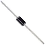
DO-201AD
ABSOLUTE RATINGS (limiting values) Symbol VRRM IP IFRM IFSM Tj Tstg Parameter Repetitive peak reverse voltage Peak forward current (1) Repetitive peak forward current Surge non repetitive forward current Tamb = 65°C δ = 0.5 tp = 5µs F = 5kHz square tp = 10 ms sinusoidal VALUE 600 4 30 80 125 - 40 to 150 Unit V A A A °C °C
Maximum operating junction temperature Storage temperature range
(1) square waveform and on infinite heatsink
TURBOSWITCH is a trademark of STMicroelectronics
November 1999 - Ed: 3C
1/5
�STTA406
THERMAL DATA Symbol Rth(j-l) Rth(j-a) Parameter Junction to lead L lead = 10mm Junction to ambient on printed circuit L lead = 10mm Max. 20 75 Unit °C/W °C/W
STATIC ELECTRICAL CHARACTERISTICS Symbol VF ** IR * Vto Rd
Test pulse :
Parameter Forward voltage drop Reverse leakage current Threshold voltage Dynamic resistance
* tp = 380 µs, δ < 2% ** tp = 5 ms, δ < 2%
Test conditions IF = 4 A VR = 0.8 VRRM Ip < 3.IF(AV) Tj = 25°C Tj = 125°C Tj = 25°C Tj = 125°C Tj = 125°C
Typ. 1.25 0.75
Max. 1.75 1.5 50 2 1.15 85
Unit V V µA mA V mΩ
To evaluate the maximum conduction losses use the following equation : P = Vto x IF(AV) + Rd x IF2(RMS) DYNAMIC ELECTRICAL CHARACTERISTICS TURN-OFF SWITCHING Symbol trr Parameter Reverse recovery time Test conditions IF = 0.5A IR = 1A Irr = 0.25A IF = 1A di/dt = -50A/µs VR = 30V Typ. 25 55 Max. Unit ns ns
TURN-ON SWITCHING Symbol tfr VFP Parameter Forward recovery time Peak forward voltage Test conditions IF = 4 A dIF/dt = 100 A/µs Measured at 1.1 x VF max. Tj = 25°C Typ. Max. 200 20 Unit ns V
2/5
�STTA406
Fig. 1: Power dissipation versus average forward current.
PF(av)(W) 3.5 3.0 2.5 2.0 1.5 1.0 0.5
T
Fig. 2: Average forward current versus ambient temperature (δ=0.5).
IF(av)(A)
δ = 0.1 δ = 0.05
δ = 0.2
δ = 0.5
δ=1
tp δ=tp/T IF(av)(A) 0.0 0.0 0.2 0.4 0.6 0.8 1.0 1.2 1.4 1.6 1.8 2.0 2.2 2.4
2.4 2.2 2.0 1.8 1.6 1.4 1.2 1.0 0.8 0.6 0.4 0.2 0.0
Rth(j-a)=Rth(j-l)
Rth(j-a)=75°C/W
T
δ=tp/T
tp
Tamb(°C) 50 75 100 125
0
25
Fig. 3: Relative variation of thermal impedance junction to ambient versus pulse duration (epoxy printed circuit board, e(Cu)=35µm), recommended pad layout).
K=[Zth(j-a)/Rth(j-a)] 1E+0
δ = 0.5 δ = 0.2 δ = 0.1
1E-1
1E-2
Single pulse
T
1E-3 1E-3
tp(s) 1E-2 1E-1 1E+0 1E+1
δ=tp/T
tp
1E+2
1E+3
Fig 4-2 : Forward voltage drop versus forward current (high level).
IFM(A) 50
Tj=125°C Typical values
Fig. 4-1: Forward voltage drop versus forward current (low level).
IFM(A) 5 4
Tj=125°C Typical values
10
Tj=125°C Maximum values
3
Tj=125°C Maximum values
Tj=25°C Maximum values
2 1
Tj=25°C Maximum values
VFM(V) 1 0.6 0.8 1.0 1.2 1.4 1.6 1.8 2.0 2.2 2.4 2.6 2.8 3.0
VFM(V) 0 0.0 0.2 0.4 0.6 0.8 1.0 1.2 1.4 1.6 1.8 2.0
3/5
�STTA406
Fig 5 : Reverse recovery time versus dIF/dt.
trr(ns) 250 225 200 175 150 125 100 75 50 25 0
IF=Ip 90% confidence Tj=125°C
Fig. 6: Reverse recovery current versus dIF/dt.
IRM(A) 15 14 13 12 11 10 9 8 7 6 5 4 3 2 1 0
IF=Ip 90% confidence Tj=125°C
dIF/dt(A/µs) 0 50 100 150 200 250 300 350 400 450 500
dIF/dt(A/µs)
0 50 100 150 200 250 300 350 400 450 500
Fig. 7: Transient peak forward voltage versus dIF/dt.
VFP(V) 25 20 15 10 5 0
IF=Ip 90% confidence Tj=25°C
Fig. 9: Junction capacitance versus reverse voltage applied (typical values).
C(pF) 20 18 16 14 12 10 8 6 4 2 0
F=1MHz Tj=25°C
dIF/dt(A/µs)
0 20 40 60 80 100 120 140 160 180 200
VR(V) 1 10 100 200
Fig. 8: Forward recovery time versus dIF/dt.
tfr(ns) 350 300 250 200 150 100 50 0
IF=Ip 90% confidence Tj=25°C Vfr=2V
dIF/dt(A/µs)
0 20 40 60 80 100 120 140 160 180 200
4/5
�STTA406
PACKAGE MECHANICAL DATA DO-201AD
B A B ØC
note 1
E
E
note 1
ØD
ØD
note 2
DIMENSIONS REF.
A B ∅C ∅D E 25.40 5.30 1.30 1.25
Millimeters Min. Max.
9.50
Inches Min.
1.000 0.209 0.051 0.049
NOTES 1 - The lead diameter ∅ D is not controlled over zone E 2 - The minimum axial length within which the device may be placed with its leads bent at right angles is 0.59"(15 mm)
Max.
0.374
Ordering type STTA406 STTA406RL
Marking STTA406 STTA406
Package DO-201AD DO-201AD
Weight 1.166g 1.166g
Base qty 600 1900
Delivery mode Ammopack Tape & reel
Cooling method: by conversion (method A) Band indicated cathode Epoxy meets UL94,V0
Information furnished is believed to be accurate and reliable. However, STMicroelectronics assumes no responsibility for the consequences of use of such information nor for any infringement of patents or other rights of third parties which may result from its use. No license is granted by implication or otherwise under any patent or patent rights of STMicroelectronics. Specifications mentioned in this publication are subject to change without notice. This publication supersedes and replaces all information previously supplied. STMicroelectronics products are not authorized for use as critical components in life support devices or systems without express written approval of STMicroelectronics.
The ST logo is a registered trademark of STMicroelectronics © 1999 STMicroelectronics - Printed in Italy - All rights reserved. STMicroelectronics GROUP OF COMPANIES Australia - Brazil - China - Finland - France - Germany - Hong Kong - India - Italy - Japan - Malaysia Malta - Morocco - Singapore - Spain - Sweden - Switzerland - United Kingdom - U.S.A. http://www.st.com 5/5
�
很抱歉,暂时无法提供与“STTA406RL”相匹配的价格&库存,您可以联系我们找货
免费人工找货- 国内价格 香港价格
- 3800+3.110773800+0.40243