STTH1002CSF
Datasheet
200 V, dual 5 A ultrafast rectifier
Features
•
•
•
175 °C maximum operation junction temperature
High surge current capability
ECOPACK2 compliant component
Application
•
•
•
DC/DC converters
Freewheeling diodes
LED Lighting
Description
The STTH1002CSF has been developed for applications requiring an optimized VF
and reverse recovery characteristics.
These characteristics make it ideal for use in secondary rectification functions, such
as DC/DC converters or lighting applications.
Product status link
STTH1002CSF
Product summary
Symbol
Value
IF(AV)
2X5A
VRRM
200 V
trr(max)
27 ns
Tj (max.)
175 °C
VF (typ.)
0.79 V
DS13535 - Rev 1 - October 2020
For further information contact your local STMicroelectronics sales office.
www.st.com
�STTH1002CSF
Characteristics
1
Characteristics
Table 1. Absolute ratings (limiting values at 25 °C, unless otherwise specified, per diode)
Symbol
Parameter
VRRM
Repetitive peak reverse voltage
IF(AV)
Average forward current, δ = 0.5
IFSM
Surge non repetitive forward current
Tstg
Storage temperature range
Tj
Value
Unit
200
V
Per diode
Tc = 160 °C
5
Per device
Tc = 160 °C
10
tp = 10 ms sinusoidal
85
A
-65 to +175
°C
+175
°C
Maximum operating junction temperature range
A
Table 2. Thermal resistance parameters
Symbol
Parameter
Rth(j-c)
Junction to case
Rth(c)
Coupling
Typ.
Per diode
2.45
Per device
1.66
Unit
°C/W
0.87
°C/W
For more information, please refer to the following application note:
•
AN5088: Rectifiers thermal management, handling and mounting recommendations
When the diodes 1 and 2 are used simultaneously:
ΔTj (diode1) = P(diode1) x Rth(j-c) (per diode) + P(diode2) x Rth(c)
Table 3. Static electrical characteristics (per diode)
Symbol
IR(1)
Parameter
Reverse leakage current
Test conditions
Tj = 25 °C
Tj = 125 °C
Tj = 25 °C
VF(2)
Forward voltage drop
Tj = 125 °C
Tj = 25 °C
Tj = 125 °C
VR = VRRM
IF = 5 A
IF = 10 A
Min.
Typ.
-
Max.
4
-
4
40
-
0.91
1.05
-
0.79
0.91
-
1.02
1.17
-
0.90
1.04
Unit
µA
V
1. Pulse test: tp = 5 ms, δ < 2%
2. Pulse test: tp = 380 µs, δ < 2%
To evaluate the conduction losses, use the following equation:
P = 0.78 x IF(AV) + 0.026 x IF2(RMS)
For more information, please refer to the following application notes related to the power losses:
•
AN604: Calculation of conduction losses in a power rectifier
•
AN4021: Calculation of reverse losses in a power diode
DS13535 - Rev 1
page 2/10
�STTH1002CSF
Characteristics
Table 4. Dynamic characteristics per diode at Tj = 25°C, unless otherwise specified
Symbol
trr
IRM
DS13535 - Rev 1
Parameter
Test conditions
Reverse recovery time
Tj = 25 °C
Reverse recovery current
Tj = 125 °C
Min.
Typ.
Max.
IF = 1 A, dIF /dt = -50 A/µs, VR = 30 V
-
28
35
IF = 1 A, dIF /dt = -100 A/µs, VR = 30 V
-
21
27
IF = 5 A, dIF/dt = -200 A/µs, VR = 160 V
-
6.3
Unit
ns
A
page 3/10
�STTH1002CSF
Characteristics (curves)
1.1
Characteristics (curves)
Figure 1. Conduction losses versus average forward
current (per diode)
Figure 2. Forward voltage drop versus forward current
(typical values, per diode)
IF(A)
PF(AV)(W)
6
1.0E+02
= 0.05
= 0.1
5
= 0.2
= 0.
=1
Tj = 150 °C
1.0E+01
4
Tj = 125 °C
3
1.0E+00
T j = 25 °C
T
2
1.0E-01
1
IF(AV)(A)
tp
=tp/T
VF(V)
0
0
1
2
3
4
5
6
Figure 3. Forward voltage drop versus forward current
(maximum values, per diode)
1.0E-02
0.0
0.5
1.0
1.5
2.0
Figure 4. Relative variation of thermal impedance junction
to case total versus pulse duration
Zth(j-c) / Rth(j-c)
IF(A)
1.0E+02
1.0
0.9
Tj = 150 °C
1.0E+01
PSMC (TO-277A)
0.8
0.7
Tj = 125 °C
0.6
1.0E+00
0.5
T j = 25 °C
0.4
0.3
1.0E-01
Single pulse
0.2
VF(V)
1.0E-02
0.0
0.5
1.0
1.5
0.1
2.0
Figure 5. Peak reverse recovery current versus dIF/dt
(typical values, per diode)
1.E-04
VR = 160 V
Tj = 125 °C
IF = IF(AV)
1.E-02
1.E-01
1.E+00
t rr (ns)
60
10
1.E-03
Figure 6. Reverse recovery time versus dIF/dt (typical
values, per diode)
IRM(A)
12
tp(s)
0.0
VR = 160 V
Tj = 125 °C
IF = IF(AV)
50
8
40
6
30
4
20
10
2
dIF/dt(A/µs)
dIF/dt(A/µs)
0
0
0
DS13535 - Rev 1
100
200
300
400
500
0
100
200
300
400
500
page 4/10
�STTH1002CSF
Characteristics (curves)
Figure 7. Reverse recovery charges versus dIF/dt (typical
values, per diode)
Figure 8. Reverse recovery softness versus dIF/dt (typical
values, per diode)
QRR (nC)
S FACTOR
0.6
200
160
VR = 160 V
Tj = 125 °C
IF = IF(AV)
VR = 160 V
Tj = 125 °C
IF = IF(AV)
0.5
0.4
120
0.3
80
0.2
40
0.1
dIF/dt(A/µs)
dIF/dt(A/µs)
0
0
0.0
100
200
300
400
500
0
Figure 9. Relative variations of dynamic parameters
versus junction temperature
200
300
400
500
Figure 10. Junction capacitance versus reverse voltage
applied (typical values, per diode)
C(pF)
2.0
1.6
100
100
VR = 160 V
IF = IF(AV)
Reference: Tj = 125 °C
F = 1 MHz
Vosc= 30 mV RMS
Tj = 25 °C
SFACTOR
1.2
0.8
IRM
0.4
QRR
10
T j (°C)
VR(V)
0.0
25
50
75
100
1
125
1
10
100
1000
Figure 11. Thermal resistance junction to ambient versus copper surface under tab (typical values, epoxy
printed board FR4, eCu = 70 µm) (PSMC (TO-277A))
Rth(j-a)(°C/W)
120
Epoxy printed circuit board, copper thickness = 70 µm
PSMC (TO-277A)
100
80
60
40
20
SCU(cm²)
0
0
DS13535 - Rev 1
1
2
3
4
5
6
7
8
9
10
page 5/10
�STTH1002CSF
Package information
2
Package information
In order to meet environmental requirements, ST offers these devices in different grades of ECOPACK packages,
depending on their level of environmental compliance. ECOPACK specifications, grade definitions and product
status are available at: www.st.com. ECOPACK is an ST trademark.
2.1
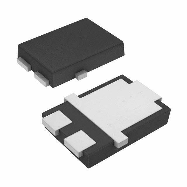
PSMC (TO-277A) package information
•
•
Epoxy meets UL94,V0
Cooling method : by conduction (C)
Figure 12. PSMC (TO-277A) package outline
DS13535 - Rev 1
page 6/10
�STTH1002CSF
PSMC (TO-277A) package information
Table 5. PSMC (TO-277A) package mechanical data
Dimensions
Millimeters
Ref.
Inches (for reference only)
Min.
Typ.
Max.
Min.
Typ.
Max.
A
1.00
1.10
1.20
0.039
0.043
0.047
b
1.05
1.20
1.35
0.041
0.047
0.053
b2
1.90
2.05
2.20
0.075
0.081
0.087
b4
0.75
0.029
C
0.15
0.23
0.40
0.006
0.009
0.016
D
4.45
4.60
4.75
0.175
0.181
0.187
D1
4.25
4.40
4.45
0.167
0.173
0.175
D2
3.40
3.60
3.70
0.134
0.142
0.146
E
6.35
6.50
6.65
0.250
0.256
0.262
E1
6.05
6.10
6.15
0.238
0.240
0.242
E2
4.50
4.60
4.70
0.177
0.181
0.185
E3
3.94
1.55
e
2.13
0.084
e1
3.33
0.131
G
1.20
0.047
G1
0.70
0.027
L
0.90
1.05
1.24
0.035
L4
0.02
0.0008
L5
0.02
0.0008
0.041
0.049
Figure 13. PSMC (TO-277A) package footprint in mm (in inches)
Note:
DS13535 - Rev 1
For package and tape orientation, reel and inner box dimensions and tape outline please check TN1173
page 7/10
�STTH1002CSF
Ordering information
3
Ordering information
Table 6. Ordering information
DS13535 - Rev 1
Order code
Marking
Package
Weight
Base qty.
Delivery mode
STTH1002CSF
TH1002C
PSMC (TO-277A)
90 mg
6000
Tape and Reel
page 8/10
�STTH1002CSF
Revision history
Table 7. Document revision history
DS13535 - Rev 1
Date
Version
29-Oct-2020
1
Changes
Initial release.
page 9/10
�STTH1002CSF
IMPORTANT NOTICE – PLEASE READ CAREFULLY
STMicroelectronics NV and its subsidiaries (“ST”) reserve the right to make changes, corrections, enhancements, modifications, and improvements to ST
products and/or to this document at any time without notice. Purchasers should obtain the latest relevant information on ST products before placing orders. ST
products are sold pursuant to ST’s terms and conditions of sale in place at the time of order acknowledgement.
Purchasers are solely responsible for the choice, selection, and use of ST products and ST assumes no liability for application assistance or the design of
Purchasers’ products.
No license, express or implied, to any intellectual property right is granted by ST herein.
Resale of ST products with provisions different from the information set forth herein shall void any warranty granted by ST for such product.
ST and the ST logo are trademarks of ST. For additional information about ST trademarks, please refer to www.st.com/trademarks. All other product or service
names are the property of their respective owners.
Information in this document supersedes and replaces information previously supplied in any prior versions of this document.
© 2020 STMicroelectronics – All rights reserved
DS13535 - Rev 1
page 10/10
�
很抱歉,暂时无法提供与“STTH1002CSF”相匹配的价格&库存,您可以联系我们找货
免费人工找货- 国内价格 香港价格
- 6000+3.418626000+0.44318
- 12000+3.1975312000+0.41452
- 18000+3.0849518000+0.39992
- 国内价格 香港价格
- 1+14.038461+1.81990
- 10+8.8730010+1.15027
- 100+5.89432100+0.76412
- 500+4.61584500+0.59838
- 1000+4.204311000+0.54503
- 2000+3.858072000+0.50015