STTH1R04-Y
Automotive ultrafast recovery diode
Datasheet - production data
Description
This device that uses ST's new 400 V planar Pt
doping technology, is specially suited for
switching mode base drive and transistor circuits.
A
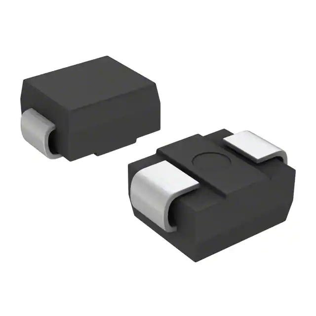
Packaged in SMB and SMA, it is intended for use
in low voltage, high frequency inverters,
freewheeling and polarity protection in
automotive applications.
K
SMA
Table 1: Device summary
SMB
Features
AEC-Q101 qualified
Negligible switching losses
Low forward and reverse recovery times
High junction temperature
ECOPACK®2 compliant component
March 2017
DocID024449 Rev 2
This is information on a product in full production.
Symbol
Value
IF(AV)
1A
VRRM
400 V
Tj (max.)
175 °C
VF (typ.)
0.9 V
trr (typ.)
14 ns
1/12
www.st.com
�Characteristics
1
STTH1R04-Y
Characteristics
Table 2: Absolute ratings (limiting values per diode at 25 °C, unless otherwise specified)
Symbol
VRRM
Parameter
Repetitive peak reverse voltage
IF(AV)
Average forward current,
δ = 0.5, square wave
IFSM
Surge non repetitive forward current
Tstg
Storage temperature range
Tj
Operating junction
Tj = -40 °C to +175 °C
SMA
Tl = 130 °C
SMB
Tl = 140 °C
Value
Unit
400
V
1.0
A
tp = 10 ms sinusoidal
30
tp = 8.3 ms sinusoidal
37
temperature(1)
A
-65 to +175
°C
-40 to +175
°C
Notes:
(1)(dP
tot/dTj)
< (1/Rth(j-a)) condition to avoid thermal runaway for a diode on its own heatsink.
Table 3: Thermal resistance parameters
Symbol
Rth(j-l)
Parameter
Junction to lead
Maximum value
SMA
30
SMB
25
Unit
°C/W
Table 4: Static electrical characteristics ( per diode)
Symbol
IR(1)
Parameter
Test conditions
Reverse leakage current
Tj = 25 °C
Tj = 125 °C
VR = VRRM
Tj = 25 °C
VF(2)
Forward voltage drop
Tj = 100 °C
IF = 1 A
Tj = 150 °C
Notes:
(1)Pulse
test: tp = 5 ms, δ < 2%
(2)Pulse
test: tp = 380 µs, δ < 2%
To evaluate the conduction losses, use the following equation:
P = 0.9 x IF(AV) + 0.250 x IF2(RMS)
2/12
DocID024449 Rev 2
Min.
Typ.
-
Max.
5
-
5
50
-
1.30
1.60
-
1.05
1.30
-
0.90
1.15
Unit
µA
V
�STTH1R04-Y
Characteristics
Table 5: Dynamic electrical characteristics per diode (Tj = 25 °C, unless otherwise specified)
Symbol
trr
Parameters
Reverse recovery time
Test conditions
Min.
Max.
IF = 1 A
dIF/dt = -50 A/μs
VR = 30 V
-
IF = 1 A
dIF/dt = -100 A/μs
VR = 30 V
-
14
20
-
2.5
3.5
2.9
IRM
Reverse recovery current
VFP
Forward recovery voltage
IF = 1 A
dIF/dt = 100 A/μs
-
Forward recovery time
IF = 1 A
dIF/dt = 100 A/μs
VFR = 1.1 x VF (max)
-
DocID024449 Rev 2
Unit
30
ns
IF = 1 A
dIF/dt = -200 A/μs
VR = 320 V
Tj = 125 °C
tfr
Typ.
A
V
50
ns
3/12
�Characteristics
1.1
STTH1R04-Y
Characteristics (curves)
Figure 1: Conduction losses versus average
forward current
1.6
Figure 2: Forward voltage drop versus forward
current
PF( AV )(W)
100.0
δ = 0.2
δ = 0.1
IFM (A)
δ = 0.5
δ = 0.05
1.4
Tj =150°C
(Maximum values)
1.2
10.0
δ=1
1.0
Tj =150°C
(Typical values)
0.8
Tj =25°C
(Maximum values)
0.6
1.0
0.4
T
0.2
IF( AV
0.0
0.0
0.2
0.4
) ( A)
0.6
δ =tp/T
0.8
VFM (V)
tp
0.1
1.0
1.2
Figure 3: Relative variation of thermal impedance
junction to case ambient versus pulse duration
(SMA)
1.0
0.0
0.8
1.2
1.6
2.0
2.4
2.8
3.2
3.6
4.0
4.4
Figure 4: Relative variation of thermal impedance
junction to case ambient versus pulse duration
(SMB)
Zth (j-a) /Rth(j-a)
Zth (j-a) /Rth(j-a)
1.0
SMA
S cu = 1cm²
0.9
0.4
SMB
Scu = 1 cm
0.9
0.8
0.8
0.7
0.7
0.6
0.6
0.5
0.5
0.4
0.4
0.3
0.3
0.2
0.2
Single pulse
0.1
t P(s)
Single pulse
0.1
t P (s)
0.0
1.E-02
0.0
1.E-03
1.E-01
1.E+00
1.E+01
1.E+02
Figure 5: Junction capacitance versus reverse
voltage applied (typical values)
100
1.E-02
1.E-01
1.E+00
1.E+01
1.E+02
1.E+03
1.E+03
Figure 6: Reverse recovery charges versus
dIF / dt (typical values)
C(pF)
QRR(nC)
40
F=1MHz
VOSC =30mVRMS
Tj=25°C
IF = 1 A
VR =320 V
36
32
28
24
10
Tj=125 °C
20
16
12
8
Tj=25 °C
4
1
10
1
4/12
dIF/dt(A/µs)
0
VR(V)
10
100
1000
DocID024449 Rev 2
100
1000
�STTH1R04-Y
Characteristics
Figure 7: Reverse recovery time versus dIF / dt
(typical values)
IRM(A)
5.0
t RR(ns)
70
65
60
55
50
45
40
35
30
25
20
15
10
5
0
Figure 8: Peak reverse recovery current versus
dIF / dt (typical values)
IF = 1 A
VR =320 V
4.5
IF = 1 A
VR =320 V
4.0
3.5
3.0
Tj=125 °C
2.5
Tj=125 °C
2.0
1.5
Tj=25 °C
1.0
10
Tj=25 °C
0.5
dIF/dt(A/µs)
100
1000
dIF/dt(A/µs)
0.0
10
Figure 9: Relative variation of dynamic parameters
versus junction temperature
Q
QRR
[Tj ]j ] // Q
QRR
[Tj =125°C]
RR;; IIRM
RM [T
RR;; IIRM
RM [T
j =125°C]
1.4
1000
Figure 10: Transient peak forward voltage versus
dIF / dt (typical values)
30
VFp(V)
IF =1 A
Tj=125 °C
IF = 1 A
VR =320 V
1.2
100
25
1.0
20
IRM
0.8
15
QRR
0.6
10
0.4
5
0.2
dIF/dt(A/µs)
Tj (°C)
0
0.0
25
50
75
100
125
150
Figure 11: Forward recovery time versus dIF / dt
(typical values)
55
t FR(ns)
0
50
150
200
250
300
350
400
450
500
Figure 12: Thermal resistance junction to ambient
total versus copper surface under each lead (SMA)
200
Rth (j -a) (°C/W)
epoxy printed board FR4, copper thickness Cu = 35 µm
IF=1 A
Tj=125 °C
50
100
SMA
45
150
40
35
30
100
25
20
15
50
10
5
SCU(cm²)
dIF/dt(A/µs)
0
0
0
50
100
150
200
250
300
350
400
450
500
DocID024449 Rev 2
0.0
0.5
1.0
1.5
2.0
2.5
3.0
3.5
4.0
4.5
5/12
5.0
�Characteristics
STTH1R04-Y
Figure 13: Thermal resistance junction to ambient
total versus copper surface under each lead (SMB)
200
Rth (j -a) (°C/W)
epoxy printed board FR4, copper thickness Cu = 35 µm
SMB
150
100
50
SCU(cm²)
0
0.0
6/12
0.5
1.0
1.5
2.0
2.5
DocID024449 Rev 2
3.0
3.5
4.0
4.5
5.0
�Package information
STTH1R04-Y
2
Package information
In order to meet environmental requirements, ST offers these devices in different grades of
ECOPACK® packages, depending on their level of environmental compliance. ECOPACK®
specifications, grade definitions and product status are available at: www.st.com.
ECOPACK® is an ST trademark.
2.1
SMA package information
Figure 14: SMA package outline
Table 6: SMA package mechanical data
Dimensions
Ref.
Millimeters
Inches
Min.
Max.
Min.
Max.
A1
1.90
2.45
0.075
0.097
A2
0.05
0.20
0.002
0.008
b
1.25
1.65
0.049
0.065
c
0.15
0.40
0.006
0.016
D
2.25
2.90
0.089
0.114
E
4.80
5.35
0.189
0.211
E1
3.95
4.60
0.156
0.181
L
0.75
1.50
0.030
0.059
DocID024449 Rev 2
7/12
�Package information
STTH1R04-Y
Figure 15: SMA recommended footprint in mm (inches)
1.4
2.63
1.4
(0.055)
(0.103)
(0.055)
1.64
(0.064)
5.43
(0.214)
8/12
DocID024449 Rev 2
�Package information
STTH1R04-Y
2.2
SMB package information
Figure 16: SMB package outline
Table 7: SMB package mechanical data
Dimensions
Ref.
Millimeters
Inches
Min.
Max.
Min.
Max.
A1
1.90
2.45
0.0748
0.0965
A2
0.05
0.20
0.0020
0.0079
b
1.95
2.20
0.0768
0.0867
c
0.15
0.40
0.0059
0.0157
D
3.30
3.95
0.1299
0.1556
E
5.10
5.60
0.2008
0.2205
E1
4.05
4.60
0.1594
0.1811
L
0.75
1.50
0.0295
0.0591
DocID024449 Rev 2
9/12
�Package information
STTH1R04-Y
Figure 17: SMB recommended Footprint
1.62
0.064
2.60
(0.102)
2.18
(0.086)
5.84
(0.230)
millimeters
(inches)
10/12
DocID024449 Rev 2
1.62
0.064
�Ordering information
STTH1R04-Y
3
Ordering information
Table 8: Ordering information
4
Order code
Marking
Package
Weight
Base qty.
Delivery mode
STTH1R04AY
HR4Y
SMA
0.068 g
5000
Tape and reel
STTH1R04UY
BR4Y
SMB
0.12 g
2500
Tape and reel
Revision history
Table 9: Document revision history
Date
Revis
ion
09-Jul-2013
1
First issue
16-Mar-2017
2
Updated Table 2: "Absolute ratings (limiting values per diode at 25 °C,
unless otherwise specified)".
Changes
DocID024449 Rev 2
11/12
�STTH1R04-Y
IMPORTANT NOTICE – PLEASE READ CAREFULLY
STMicroelectronics NV and its subsidiaries (“ST”) reserve the right to make changes, corrections, enhancements, modifications, and
improvements to ST products and/or to this document at any time without notice. Purchasers should obtain the latest relevant information on ST
products before placing orders. ST products are sold pursuant to ST’s terms and conditions of sale in place at the time of order
acknowledgement.
Purchasers are solely responsible for the choice, selection, and use of ST products and ST assumes no liability for application assistance or the
design of Purchasers’ products.
No license, express or implied, to any intellectual property right is granted by ST herein.
Resale of ST products with provisions different from the information set forth herein shall void any warranty granted by ST for such product.
ST and the ST logo are trademarks of ST. All other product or service names are the property of their respective owners.
Information in this document supersedes and replaces information previously supplied in any prior versions of this document.
© 2017 STMicroelectronics – All rights reserved
12/12
DocID024449 Rev 2
�
很抱歉,暂时无法提供与“STTH1R04UY”相匹配的价格&库存,您可以联系我们找货
免费人工找货- 国内价格
- 1+3.81560
- 10+2.54380
- 30+2.11980
- 国内价格 香港价格
- 1+6.209971+0.80166
- 10+3.8673710+0.49925
- 100+2.47333100+0.31929
- 500+1.87348500+0.24185
- 1000+1.679741000+0.21684