STTH20004TV1
Ultrafast high voltage rectifier
Datasheet - production data
Features
• Ultrafast switching
K1
• Low reverse current
• Low thermal resistance
A1
• Reduces switching and conduction losses
• Insulated package:
– Electrical insulation = 2500 V rms
– Capacitance = 189 pF
K2
• ECOPACK®2 compliant component
A2
Description
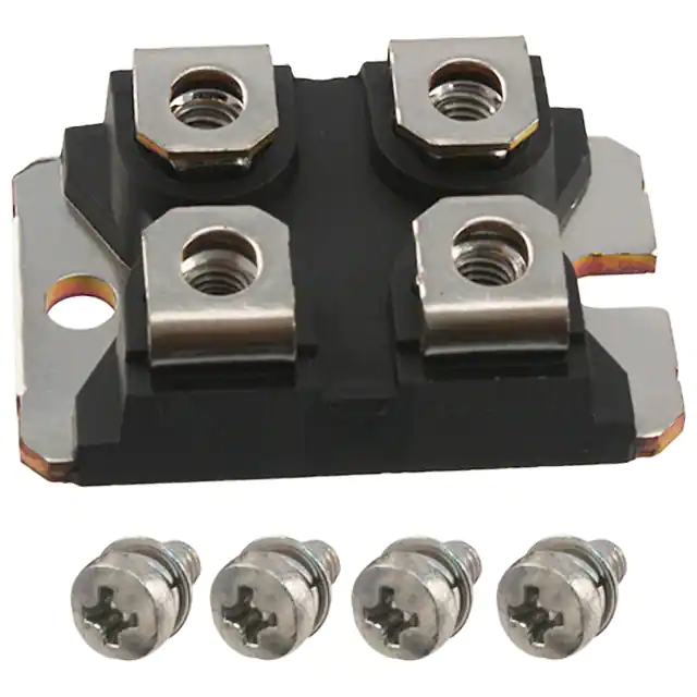
ISOTOP
STTH20004TV1
The STTH20004TV1 uses ST new 400 V
technology and is specially suited for use in
switching power supplies, welding equipment,
and industrial applications, as an output
rectification diode.
Table 1. Device summary
Symbol
Value
IF(AV)
Up to 2 x 120 A
VRRM
400 V
Tj(max)
150 °C
VF (typ)
0.83 V
trr (max)
60 ns
June 2014
This is information on a product in full production.
DocID11819 Rev 3
1/9
www.st.com
9
�Characteristics
1
STTH20004TV1
Characteristics
Table 2. Absolute ratings (limiting values, per diode)
Symbol
Parameter
Value
Unit
VRRM
Repetitive peak reverse voltage
400
V
IF(RMS)
Forward rms current
200
A
IF(AV)
Average forward current, δ = 0.5
IFSM
Surge non repetitive forward current
Tstg
Storage temperature range
Tj
Tc = 75 °C
Per diode
100
Tc = 55 °C
Per diode
120
A
tp = 10 ms Sinusoidal
900
A
-55 to + 150
°C
150
°C
Maximum
Unit
Maximum operating junction temperature
Table 3. Thermal parameter
Symbol
Parameter
Rth(j-c)
Junction to case
R th(c)
Coupling
Per diode
0.60
Total
0.35
°C/W
0.10
When the diodes 1 and 2 are used simultaneously:
Δ Tj (diode1) = P(diode1) x Rth(j-c) (per diode) + P(diode2) x Rth(c)
Table 4.
Symbol
Static electrical characteristics (per diode)
Parameter
IR(1)
Reverse leakage current
VF(2)
Forward voltage drop
Test conditions
Tj = 25 °C
Tj = 125 °C
Tj = 25 °C
Tj = 150 °C
Min.
Typ.
Unit
100
VR = VRRM
µA
100
1000
1.2
IF = 100 A
V
0.83
1. Pulse test: tp = 5 ms, δ < 2%
2. Pulse test: tp = 380 µs, δ < 2%
To evaluate the maximum conduction losses use the following equation:
P = 0.8 x IF(AV) + 0.002 IF2(RMS)
2/9
Max.
DocID11819 Rev 3
1.0
�STTH20004TV1
Characteristics
Table 5. Dynamic characteristics
Symbol
Reverse recovery time
trr
Test conditions
Parameter
Tj = 25 °C
Forward recovery time
tfr
VFP
Forward recovery voltage
IRM
Reverse recovery current
Sfactor
Typ.
Max.
IF = 1 A,
dIF/dt = 50 A/µs,
VR = 30 V
75
100
IF = 1 A,
dIF/dt = 200 A/µs,
VR = 30 V
45
IF = 100 A,
dIF/dt = 200 A/µs
VFR = 1.1 x VFmax
Tj = 125 °C
IF = 100 A,
dIF/dt = 100 A/µs,
VR = 200 V
δ=1
δ=0.5
δ=0.2
140
V
18
A
0.4
-
180
Tj=150°C
(Maximum values)
140
δ=0.05
ns
2.6
160
δ=0.1
120
800
I FM (A)
200
160
60
Figure 2. Forward voltage drop versus forward
current (per diode)
P(W)
180
Unit
ns
Tj = 25 °C
Figure 1. Conduction losses versus average
forward current (per diode)
Min.
120
100
100
Tj=150°C
(Typical values)
80
80
60
60
T
40
40
20
δ=tp/T
I F(AV) (A)
0
0
10
20
30
40
50
60
70
80
tp
Zth(j-c) /Rth( j-c)
0.0
Single pulse
40
0.7
35
0.6
30
0.5
25
0.4
20
0.3
15
0.2
10
1.E-01
1.E+01
0.8
1.0
1.2
1.4
dIF/dt(A/µs)
0
1.E+00
0.6
IF=IF(AV)
VR=200V
Tj=125°C
5
t P (s)
1.E-02
0.4
IRM (A)
45
0.8
0.0
1.E-03
0.2
Figure 4. Peak reverse recovery current versus
dIF/dt (typical values, per diode)
50
1.0
0.1
Tj=25°C
(Maximum values)
VFM (V)
0
90 100 110 120 130 140 150
Figure 3. Relative variation of thermal
impedance junction to case versus pulse
duration
0.9
20
0
DocID11819 Rev 3
50
100
150
200
250
300
350
400
450
500
3/9
�Characteristics
STTH20004TV1
Figure 5. Reverse recovery time versus dIF/dt
(typical values, per diode)
Figure 6. Reverse recovery charges versus
dIF/dt (typical values, per diode)
Q rr (nC)
t rr (ns)
300
3500
IF=IF(AV)
VR=200V
Tj=125°C
250
IF=IF(AV)
VR=200V
Tj=125°C
3000
2500
200
2000
150
1500
100
1000
50
500
dIF/dt(A/µs)
0
0
50
100
150
200
250
300
400
450
500
0
Figure 7. Reverse recovery time versus dIF/dt
(typical values, per diode)
0.8
dIF/dt(A/µs)
0
350
S FACTOR
50
100
150
200
250
300
350
400
450
500
Figure 8. Relative variations of dynamic
parameters versus junction temperature
1.6
IF < 2 x IF(AV)
VR=200V
Tj=125°C
0.7
SFACTOR
1.4
1.2
0.6
1.0
0.5
0.8
0.4
tRR
0.6
0.3
IRM
0.4
0.2
QRR
0.2
0.1
dIF/dt(A/µs)
0.0
0
50
100
150
200
250
300
IF=IF(AV)
VR=200V
Reference: Tj=125°C
Tj (°C)
0.0
350
400
450
500
25
50
75
100
125
Figure 9. Transient peak forward voltage versus Figure 10. Forward recovery time versus dIF/dt
dIF/dt (typical values, per diode)
(typical values, per diode)
6.0
t fr (ns)
VFP (V)
1800
IF=IF(AV)
Tj=125°C
5.5
5.0
4.5
1400
4.0
1200
3.5
1000
3.0
2.5
800
2.0
600
1.5
400
1.0
200
dIF/dt(A/µs)
0.5
0.0
dIF /dt(A/µs)
0
0
4/9
IF=IF(AV)
VFR=1.1 x VF max.
Tj=125°C
1600
50
100
150
200
250
300
350
400
450
500
0
DocID11819 Rev 3
50
100
150
200
250
300
350
400
450
500
�STTH20004TV1
Characteristics
Figure 11. Reverse recovery time versus dIF/dt (typical values, per diode)
C(pF)
10000
F=1MHz
VOSC=30mVRMS
Tj=25°C
1000
VR(V)
100
1
10
100
DocID11819 Rev 3
1000
5/9
�Package information
2
STTH20004TV1
Package information
•
Epoxy meets UL94, V0
•
Lead-free package
•
Cooling method: by conduction (C)
In order to meet environmental requirements, ST offers these devices in different grades of
ECOPACK® packages, depending on their level of environmental compliance. ECOPACK®
specifications, grade definitions and product status are available at: www.st.com.
ECOPACK® is an ST trademark.
Figure 12. ISOTOP dimension definitions
6/9
DocID11819 Rev 3
�STTH20004TV1
Package information
Table 6. ISOTOP dimension values
Dimensions
Ref.
Millimeters
Min.
Typ.
Inches
Max.
Min.
Typ.
Max.
A
11.80
12.20
0.465
0.480
A1
8.90
9.10
0.350
0.358
B
7.8
8.20
0.307
0.323
C
0.75
0.85
0.030
0.033
C2
1.95
2.05
0.077
0.081
D
37.80
38.20
1.488
1.504
D1
31.50
31.70
1.240
1.248
E
25.15
25.50
0.990
1.004
E1
23.85
24.15
0.939
0.951
E2
24.80
0.976
G
14.90
15.10
0.587
0.594
G1
12.60
12.80
0.496
0.504
G2
3.50
4.30
0.138
0.169
F
4.10
4.30
0.161
0.169
F1
4.60
5.00
0.181
0.197
P
4.00
4.30
0.157
0.69
P1
4.00
4.40
0.157
0.173
S
30.10
30.30
1.185
1.193
DocID11819 Rev 3
7/9
�Ordering information
3
STTH20004TV1
Ordering information
Table 7. Ordering information
Order code
Marking
Package
Weight
Base qty(1)
Delivery mode
STTH20004TV1
STTH20004TV1
ISOTOP
27 g
(without screws)
10
(with screws)
Tube
1. This product is supplied with 40 terminal screws and washers for each tube. The screws and
washers are supplied in a separate pack with the order.
4
Revision history
Table 8. Document revision history
8/9
Date
Revision
Changes
18-Oct-2005
1
First issue.
15-Sep-2011
2
Added insulated package information in Features.
20-Jun-2014
3
Updated ECOPACK® statement, Table 2 and Table 3.
DocID11819 Rev 3
�STTH20004TV1
Please Read Carefully:
Information in this document is provided solely in connection with ST products. STMicroelectronics NV and its subsidiaries (“ST”) reserve the
right to make changes, corrections, modifications or improvements, to this document, and the products and services described herein at any
time, without notice.
All ST products are sold pursuant to ST’s terms and conditions of sale.
Purchasers are solely responsible for the choice, selection and use of the ST products and services described herein, and ST assumes no
liability whatsoever relating to the choice, selection or use of the ST products and services described herein.
No license, express or implied, by estoppel or otherwise, to any intellectual property rights is granted under this document. If any part of this
document refers to any third party products or services it shall not be deemed a license grant by ST for the use of such third party products
or services, or any intellectual property contained therein or considered as a warranty covering the use in any manner whatsoever of such
third party products or services or any intellectual property contained therein.
UNLESS OTHERWISE SET FORTH IN ST’S TERMS AND CONDITIONS OF SALE ST DISCLAIMS ANY EXPRESS OR IMPLIED
WARRANTY WITH RESPECT TO THE USE AND/OR SALE OF ST PRODUCTS INCLUDING WITHOUT LIMITATION IMPLIED
WARRANTIES OF MERCHANTABILITY, FITNESS FOR A PARTICULAR PURPOSE (AND THEIR EQUIVALENTS UNDER THE LAWS
OF ANY JURISDICTION), OR INFRINGEMENT OF ANY PATENT, COPYRIGHT OR OTHER INTELLECTUAL PROPERTY RIGHT.
ST PRODUCTS ARE NOT DESIGNED OR AUTHORIZED FOR USE IN: (A) SAFETY CRITICAL APPLICATIONS SUCH AS LIFE
SUPPORTING, ACTIVE IMPLANTED DEVICES OR SYSTEMS WITH PRODUCT FUNCTIONAL SAFETY REQUIREMENTS; (B)
AERONAUTIC APPLICATIONS; (C) AUTOMOTIVE APPLICATIONS OR ENVIRONMENTS, AND/OR (D) AEROSPACE APPLICATIONS
OR ENVIRONMENTS. WHERE ST PRODUCTS ARE NOT DESIGNED FOR SUCH USE, THE PURCHASER SHALL USE PRODUCTS AT
PURCHASER’S SOLE RISK, EVEN IF ST HAS BEEN INFORMED IN WRITING OF SUCH USAGE, UNLESS A PRODUCT IS
EXPRESSLY DESIGNATED BY ST AS BEING INTENDED FOR “AUTOMOTIVE, AUTOMOTIVE SAFETY OR MEDICAL” INDUSTRY
DOMAINS ACCORDING TO ST PRODUCT DESIGN SPECIFICATIONS. PRODUCTS FORMALLY ESCC, QML OR JAN QUALIFIED ARE
DEEMED SUITABLE FOR USE IN AEROSPACE BY THE CORRESPONDING GOVERNMENTAL AGENCY.
Resale of ST products with provisions different from the statements and/or technical features set forth in this document shall immediately void
any warranty granted by ST for the ST product or service described herein and shall not create or extend in any manner whatsoever, any
liability of ST.
ST and the ST logo are trademarks or registered trademarks of ST in various countries.
Information in this document supersedes and replaces all information previously supplied.
The ST logo is a registered trademark of STMicroelectronics. All other names are the property of their respective owners.
© 2014 STMicroelectronics - All rights reserved
STMicroelectronics group of companies
Australia - Belgium - Brazil - Canada - China - Czech Republic - Finland - France - Germany - Hong Kong - India - Israel - Italy - Japan Malaysia - Malta - Morocco - Philippines - Singapore - Spain - Sweden - Switzerland - United Kingdom - United States of America
www.st.com
DocID11819 Rev 3
9/9
�


 工商网监
湘ICP备2023018690号
工商网监
湘ICP备2023018690号
