STTH60W03C
High efficiency rectifier
Datasheet - production data
Description
A1
K
The STTH60W03C uses ST 300 V technology. It
is especially suited to be used for DC/DC and
DC/AC converters in secondary stage of
MIG/MMA/TIG welding machine. Housed in ST's
TO-247, this device offers high power integration
for all welding machines and industrial
applications.
A2
Table 1: Device summary
A2
K
Symbol
Value
IF(AV)
2 x 30 A
VRRM
300 V
Tj
175 °C
Features
VF (typ.)
0.94 V
trr (typ.)
25 ns
A1
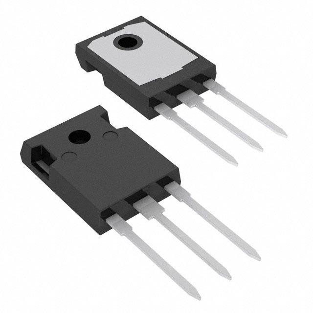
TO-247
Ultrafast switching
Low reverse current
Low thermal resistance
Reduced switching losses
ECOPACK®2 compliant component
February 2018
DocID023144 Rev 2
This is information on a product in full production.
1/9
www.st.com
�Characteristics
1
STTH60W03C
Characteristics
Table 2: Absolute ratings (limiting values, per diode, limiting values at 25°C, unless otherwise
specified)
Symbol
Parameter
Value
Unit
VRRM
Repetitive peak reverse voltage
300
V
IF(RMS)
Forward rms current
50
A
Average forward current δ = 0.5,
square wave
Tc = 110 °C
Per diode
30
A
IF(AV)
Tc = 95 °C
Per device
60
A
IFSM
Surge non repetitive forward current
tp = 10 ms sinusoidal
280
A
Tstg
Storage temperature range
-65 to +175
°C
+175
°C
Tj
Maximum operating junction temperature range
Table 3: Thermal parameters
Symbol
Rth(j-c)
Rth(c)
Parameter
Junction to case
Max. value
Unit
Per diode
1.5
°C/W
Total
0.9
°C/W
0.3
°C/W
Coupling
When the diodes 1 and 2 are used simultaneously:
ΔTj (diode1) = P(diode1) x Rth(j-c) (per diode) + P(diode2) x Rth(c)
Table 4: Static electrical characteristics (per diode)
Symbol
IR(1)
Parameter
Test conditions
Reverse leakage current
Tj = 25 °C
Tj = 125 °C
Tj = 25 °C
VF(2)
Forward voltage drop
Tj = 150 °C
Tj = 25 °C
Tj = 150 °C
VR = VRRM
IF = 30 A
IF = 60 A
Notes:
(1)Pulse
test: tp = 5 ms, δ < 2%
(2)Pulse
test: tp = 380 μs, δ < 2 %
To evaluate the conduction losses, use the following equation:
P = 0.85 x IF(AV) + 0.010 x IF2(RMS)
2/9
DocID023144 Rev 2
Min.
Typ.
-
20
20
-
200
Unit
µA
1.45
0.94
-
Max.
1.15
1.7
1.18
1.45
V
�STTH60W03C
Characteristics
Table 5: Dynamic electrical characteristics (per diode)
Symbol
Parameters
IRM
Reverse recovery current
Tj = 125 °C
IF = 30 A,
VR = 200 V,
dIF/dt = -200 A/μs
-
7
QRR
Reverse recovery charge
Tj = 125 °C
IF = 30 A,
VR = 200 V,
dIF/dt = -200 A/μs
-
180
Sfactor
Softness factor
Tj = 125 °C
IF = 30 A,
VR = 200 V,
dIF/dt = -200 A/μs
-
0.3
trr
Reverse recovery time
Tj = 25 °C
IF = 1 A,
dIF/dt = -100 A/μs,
VR = 30 V
-
25
tfr
Forward recovery time
Tj = 25 °C
IF = 30 A,
dIF/dt = 200 A/μs,
VFR = 1.5 V
VFP
Test conditions
Forward recovery voltage
DocID023144 Rev 2
Min.
Typ.
-
2.0
Max.
9
Unit
A
nC
35
ns
180
ns
3.0
V
3/9
�Characteristics
1.1
STTH60W03C
Characteristics (curves)
Figure 1: Average forward power dissipation
versus average forward current (per diode)
Figure 2: Forward voltage drop versus forward
current (per diode)
IFM(A)
PF(AV)(W)
1000.0
50
δ = 0.2
45
δ=1
δ = 0.5
Tj = 150 °C
(Maximum values)
δ = 0. 1
40
100.0
δ = 0. 05
35
Tj = 150 °C
(Typical values)
Tj = 25 °C
(Maximum values)
30
10.0
25
20
15
1.0
T
10
5
δ = tp/T
VFM (V)
IF(AV)(A)
tp
0.1
0.0
0
0
5
10
15
20
25
30
35
40
Figure 3: Relative variation of thermal impedance
junction to case versus pulse duration
0.5
1.0
1.5
2.0
2.5
3.0
Figure 4: Peak reverse recovery current versus
dIF/dt (typical values, per diode)
Zth(j-c) /Rth(j-c)
IRM (A)
1.0
16
0.9
IF = IF(AV)
VR = 200 V
Tj = 125 °C
14
0.8
12
0.7
0.6
10
0.5
8
0.4
6
0.3
4
Single pulse
0.2
2
0.1
dI F /dt(A/µs)
t p(s)
0
0.0
1.E-04
1.E-03
1.E-02
1.E-01
1.E+00
Figure 5: Reverse recovery time versus dIF/dt
(typical values, per diode)
0
50
100
150
200
250
300
350
400
450
500
Figure 6: Reverse recovery charges versus dIF/dt
(typical values, per diode)
Q RR(nC)
t rr (ns)
350
100
IF = I F(AV)
V R = 200 V
T j = 125 °C
90
80
IF = IF(AV)
VR = 200 V
Tj = 125 °C
300
250
70
60
200
50
150
40
30
100
20
50
10
dI F /dt(A/µs)
dI F /dt(A/µs)
0
0
0
4/9
50
100
150
200
250
300
350
400
450
500
DocID023144 Rev 2
0
50
100
150
200
250
300
350
400
450
500
�STTH60W03C
Characteristics
Figure 7: Relative variation of dynamic parameters
versus junction temperature
Figure 8: Reverse recovery softness factor versus
dIF/dt (typical values, per diode)
0.8
2. 5
IF = I F(AV)
VR = 200 V
Reference: Tj =125 °C
SFACTOR
2. 0
0.7
0.6
0.5
1. 5
0.4
0.3
1. 0
0.2
IRM
0. 5
0.1
Tj (°C)
QRR
0. 0
25
50
75
100
0.0
0
125
50
100
150
200
250
300
350
400
450
500
Figure 10: Transient peak forward voltage versus
dIF/dt (typical values, per diode)
Figure 9: Transient peak forward voltage versus
dIF/dt (typical values, per diode)
VFP (V)
t fr (ns)
5
180
IF =I F(AV)
Tj=125 °C
IF = IF(AV)
VFR = 1.5 V
Tj = 125 °C
160
140
4
120
3
100
80
2
60
40
1
20
0
150
dI F/dt(A/µs)
dI F/dt(A/µs)
200
250
300
350
400
450
500
0
100
150
200
250
300
350
400
450
Figure 11: Junction capacitance versus reverse
voltage applied (typical values, per diode)
C(pF)
1000
F = 1 MHz
VOSC = 30 mVRMS
Tj = 25 °C
100
VR(V)
10
1
10
DocID023144 Rev 2
100
1000
5/9
500
�Package information
2
STTH60W03C
Package information
In order to meet environmental requirements, ST offers these devices in different grades of
ECOPACK® packages, depending on their level of environmental compliance. ECOPACK®
specifications, grade definitions and product status are available at: www.st.com.
ECOPACK® is an ST trademark.
2.1
Epoxy meets UL94, V0
Cooling method: by conduction (C)
Recommended torque value: 0.8 N·m (TO-247)
Maximum torque value: 1.0 N·m (TO-247)
TO-247 with Inches package information
Figure 12: TO-247 package outline
0075325_8
6/9
DocID023144 Rev 2
�Package information
STTH60W03C
Table 6: TO-247 package mechanical data
Dimensions
Ref.
Millimeters
Min.
Typ.
Inches
Max.
Min.
Typ.
Max.
A
4.85
5.15
0.191
0.203
A1
2.20
2.60
0.086
0.102
b
1.00
1.40
0.039
0.055
b1
2.00
2.40
0.078
0.094
b2
3.00
3.40
0.118
0.133
c
0.40
0.80
0.015
0.031
D(1)
19.85
20.15
0.781
0.793
E
15.45
15.75
0.608
0.620
e
5.30
5.60
0.209
L
14.20
14.80
0.559
0.582
L1
3.70
4.30
0.145
0.169
L2
5.45
18.50
0.215
0.220
0.728
ØP(2)
3.55
3.65
0.139
0.143
ØR
4.50
5.50
0.177
0.217
S
5.30
5.70
0.209
5.50
0.216
0.224
Notes:
(1)Dimension
(2)Resin
D plus gate protusion does not exceed 20.5 mm
thickness around the mounting hole is not less than 0.9 mm.
DocID023144 Rev 2
7/9
�Ordering information
3
STTH60W03C
Ordering information
Table 7: Ordering information
4
Order code
Marking
Package
Weight
Base qty.
Delivery mode
STTH60W03CW
STTH60W03CW
TO-247
4.43 g
50
Tube
Revision history
Table 8: Document revision history
8/9
Date
Revision
Changes
07-Sep-2004
1
First issue.
08-Feb-2018
2
Updated Description and package information.
DocID023144 Rev 2
�STTH60W03C
IMPORTANT NOTICE – PLEASE READ CAREFULLY
STMicroelectronics NV and its subsidiaries (“ST”) reserve the right to make changes, corrections, enhancements, modifications, and
improvements to ST products and/or to this document at any time without notice. Purchasers should obtain the latest relevant information on ST
products before placing orders. ST products are sold pursuant to ST’s terms and conditions of sale in place at the time of order
acknowledgement.
Purchasers are solely responsible for the choice, selection, and use of ST products and ST assumes no liability for application assistance or the
design of Purchasers’ products.
No license, express or implied, to any intellectual property right is granted by ST herein.
Resale of ST products with provisions different from the information set forth herein shall void any warranty granted by ST for such product.
ST and the ST logo are trademarks of ST. All other product or service names are the property of their respective owners.
Information in this document supersedes and replaces information previously supplied in any prior versions of this document.
© 2018 STMicroelectronics – All rights reserved
DocID023144 Rev 2
9/9
�
很抱歉,暂时无法提供与“STTH60SW03CW”相匹配的价格&库存,您可以联系我们找货
免费人工找货- 国内价格 香港价格
- 600+10.63456600+1.37558