STV160NF02L
N-CHANNEL 20V - 0.0016Ω - 160A PowerSO-10
STripFET™ II POWER MOSFET
TYPE
STV160NF02L
VDSS
RDS(on)
ID
20 V
< 0.0025 Ω
160 A
TYPICAL RDS(on) = 0.0016 Ω
LOW THRESHOLD DRIVE
ULTRA LOW ON-RESISTANCE
ULTRA FAST SWITCHING
100% AVALANCHE TESTED
VERY LOW GATE CHARGE
LOW PROFILE, VERY LOW PARASITIC
INDUCTANCE PowerSO-10 PACKAGE
■
■
■
■
■
■
■
10
1
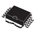
PowerSO-10
DESCRIPTION
The STV160NF02L represents the second generation of Application Specific STMicroelectronics
well established STripFET™ process based on a
very unique strip layout design. The resulting
MOSFET shows unrivalled high packing density
with ultra low on-resistance and superior switching
charactestics. Process simplification also translates into improved manufacturing reproducibility.
This device is particularly suitable for high current,
low voltage switching application where efficiency
is crucial
)
s
(
ct
)
s
t(
INTERNAL SCHEMATIC DIAGRAM
c
u
d
e
t
le
o
r
P
o
s
b
O
-
CONNECTION DIAGRAM (TOP VIEW)
APPLICATIONS
■ BUCK CONVERTERS IN HIGH
PERFORMANCE TELECOM AND VRMs DCDC CONVERTERS
u
d
o
r
P
e
ABSOLUTE MAXIMUM RATINGS
Symbol
Parameter
Value
Unit
Drain-source Voltage (VGS = 0)
20
V
Drain-gate Voltage (RGS = 20 kΩ)
20
V
t
e
l
o
VDS
VDGR
bs
O
VGS
Gate- source Voltage
± 15
V
ID(**)
Drain Current (continuos) at TC = 25°C
160
A
ID
Drain Current (continuos) at TC = 100°C
113
A
IDM (�)
PTOT
EAS (1)
Tstg
Tj
Drain Current (pulsed)
640
A
Total Dissipation at TC = 25°C
210
W
Derating Factor
1.4
W/°C
Single Pulse Avalanche Energy
Storage Temperature
Max. Operating Junction Temperature
(● ) Pulse width limited by safe operating area
February 2004
1.5
J
–65 to 175
°C
175
°C
(1) Starting Tj=25°C , ID = 80A, VDD = 20V
(**)Limited only maximum junction temperature allowed by
PowerSO-10
1/8
�STV160NF02L
THERMAL DATA
Rthj-case
Thermal Resistance Junction-case Max
Rthj-amb
Tl
0.71
°C/W
Thermal Resistance Junction-ambient Max
50
°C/W
Maximum Lead Temperature For Soldering Purpose
300
°C
ELECTRICAL CHARACTERISTICS (TCASE = 25 °C UNLESS OTHERWISE SPECIFIED)
OFF
Symbol
V(BR)DSS
IDSS
IGSS
Parameter
Test Conditions
Min.
Typ.
Max.
20
ID = 250 µA, VGS = 0
V
Zero Gate Voltage
Drain Current (VGS = 0)
VDS = Max Rating
1
µA
VDS = Max Rating, TC = 125 °C
10
µA
Gate-body Leakage
Current (VDS = 0)
VGS = ± 15 V
±100
nA
ON (1)
Symbol
Parameter
Test Conditions
Min.
VGS(th)
Gate Threshold Voltage
VDS = VGS, ID = 250µA
RDS(on)
Static Drain-source On
Resistance
VGS = 10 V, ID = 80 A
VGS = 10 V, ID = 45 A
VGS = 10 V, ID = 20 A
VGS = 8 V, ID = 80 A
VGS = 5 V, ID = 40 A
VGS = 10 V, ID=80 A;Tj = 175 °C
VGS = 8 V, ID=80 A; Tj = 175 °C
VGS = 5 V, ID=40 A; Tj = 175 °C
On State Drain Current
DYNAMIC
gfs (1)
Test Conditions
Pr
od
1.6
1.56
1.35
1.7
3.5
)
s
t(
Max.
2.5
2.5
2.5
3.5
6
5.7
7
11.4
160
Min.
Unit
V
mΩ
mΩ
mΩ
mΩ
mΩ
mΩ
mΩ
mΩ
A
Typ.
Max.
Unit
Forward Transconductance
VDS > ID(on) x RDS(on)max,
ID = 80A
210
S
Gate resistance
VDS = 0 V, f = 1 MHz, VGS = 0
0.5
Ω
Ciss
Coss
Crss
Input Capacitance
Output Capacitance
Reverse Transfer
Capacitance
VDS = 15 V, f = 1 MHz, VGS = 0
Ciss
Coss
Crss
Input Capacitance
Output Capacitance
Reverse Transfer
Capacitance
VDS = 0 V, f = 1 MHz, VGS = 0
LS
Internal Source Inductance
From the Lead End (6mm from
Package Body) to the Die
Center
LD
Internal Drain Inductance
Rg
r
P
e
t
e
l
o
s
b
O
2/8
Parameter
VDS > ID(on) x RDS(on)max,
VGS = 10V
)
s
(
ct
u
d
o
Symbol
o
s
b
O
-
uc
Typ.
1
e
t
le
ID(on)
Unit
Drain-source
Breakdown Voltage
4800
3000
680
7000
12300
4200
4
pF
pF
pF
pF
pF
pF
nH
Not Available on Surface Mounting
Package
�STV160NF02L
ELECTRICAL CHARACTERISTICS (CONTINUED)
SWITCHING ON
Symbol
td(on)
tr
Parameter
Test Conditions
Rise Time
Qg
Qgs
Qgd
Min.
VDD = 10 V, ID = 80 A
RG = 4.7Ω VGS = 10V
(see test circuit, Figure 3)
Turn-on Delay Time
Total Gate Charge
Gate-Source Charge
Gate-Drain Charge
VDD = 16 V, ID = 160 A,
VGS = 10 V
Typ.
Max.
Unit
28
ns
800
ns
115
15
45
160
nC
nC
nC
Typ.
Max.
Unit
SWITCHING OFF
Symbol
Parameter
Test Conditions
Min.
td(off)
tf
Turn-off-Delay Time
Fall Time
VDD = 10 V, ID = 80 A,
RG = 4.7Ω, VGS = 10 V
(see test circuit, Figure 5)
80
240
td(off)
tr(Voff)
tf
tc
Turn-off Delay Time
Off-voltage Rise Time
Fall Time
Cross-over Time
Vclamp = 16 V, ID = 40 A
RG = 4.7Ω, VGS = 10V
80
40
140
200
c
u
d
e
t
le
SOURCE DRAIN DIODE
Symbol
ISD
ISDM (1)
VSD (2)
trr
Qrr
IRRM
Parameter
Test Conditions
Source-drain Current (pulsed)
Min.
Typ.
b
O
-
ISD = 160 A, VGS = 0
Forward On Voltage
Reverse Recovery Time
Reverse Recovery Charge
Reverse Recovery Current
ISD = 80 A, di/dt = 100A/µs,
VDD = 15V, Tj = 25°C
(see test circuit, Figure 5)
)
s
(
ct
)
s
t(
o
r
P
so
Source-drain Current
ns
ns
Max.
Unit
160
A
640
A
1.5
90
225
5
ns
ns
ns
ns
V
ns
nC
A
Note: 1. Pulsed: Pulse duration = 300 µs, duty cycle 1.5 %.
2. Pulse width limited by safe operating area.
r
P
e
u
d
o
Safe Operating Area
Thermal Impedance
t
e
l
o
s
b
O
3/8
�STV160NF02L
Output Characteristics
Tranfer Characteristics
Tranconductance
Static Drain-Source On Resistance
c
u
d
e
t
le
)
s
(
ct
u
d
o
r
P
e
Gate Charge vs Gate-source Voltage
t
e
l
o
s
b
O
4/8
o
r
P
o
s
b
O
-
Capacitance Variations
)
s
t(
�STV160NF02L
Normalized Gate Thereshold Voltage vs Temp.
Normalized On Resistance vs Temperature
Source-drain Diode Forward Characteristics
c
u
d
e
t
le
)
s
(
ct
u
d
o
r
P
e
)
s
t(
o
r
P
o
s
b
O
-
Basic Schematic For Motherboard VRM Whith
Synchronous Rectification
Basic Schematic Mosfets Switch Used In
Secondary Side Of a Froward Convert
t
e
l
o
s
b
O
5/8
�STV160NF02L
Fig. 1: Unclamped Inductive Load Test Circuit
Fig. 2: Unclamped Inductive Waveform
Fig. 3: Switching Times Test Circuit For
Resistive Load
Fig. 4: Gate Charge test Circuit
c
u
d
e
t
le
)
s
(
ct
u
d
o
o
s
b
O
-
Fig. 5: Test Circuit For Inductive Load Switching
And Diode Recovery Times
r
P
e
t
e
l
o
s
b
O
6/8
o
r
P
)
s
t(
�STV160NF02L
PowerSO-10 MECHANICAL DATA
mm
DIM.
MIN.
inch
TYP.
MAX.
MIN.
TYP.
MAX.
A
3.35
3.65
0.132
0.144
A1
0.00
0.10
0.000
0.004
B
0.40
0.60
0.016
0.024
C
0.35
0.55
0.013
0.022
D
9.40
9.60
0.370
0.378
D1
7.40
7.60
0.291
e
1.27
0.300
0.050
E
9.30
9.50
0.366
0.374
E1
7.20
7.40
0.283
0.291
E2
7.20
7.60
0.283
0.300
E3
6.10
6.35
0.240
0.250
E4
5.90
6.10
0.232
F
1.25
1.35
0.049
h
0.50
H
13.80
L
1.20
q
0.543
1.80
0.047
d
o
r
P
e
let
1.70
α
0.240
0.002
14.40
uc
)
s
t(
0.053
0.567
0.071
0.067
0o
8o
o
s
b
O
B
1
r
P
e
s
b
O
t
e
l
o
h
e
0.25
5
B
=
E4
=
=
E1
=
=
=
u
d
o
E3
=
E2
=
E
0.10 A B
=
=
=
H
6
=
)
s
(
ct
10
SEATING
PLANE
DETAIL "A"
A
C
M
Q
D
= D1 =
=
=
SEATING
PLANE
A
F
A1
A1
L
DETAIL "A"
α
0068039-C
7/8
�STV160NF02L
c
u
d
e
t
le
)
s
(
ct
)
s
t(
o
r
P
o
s
b
O
-
u
d
o
r
P
e
t
e
l
o
Information furnished is believed to be accurate and reliable. However, STMicroelectronics assumes no responsibility for the
consequences of use of such information nor for any infringement of patents or other rights of third parties which may result from
its use. No license is granted by implication or otherwise under any patent or patent rights of STMicroelectronics. Specifications
mentioned in this publication are subject to change without notice. This publication supersedes and replaces all information
previously supplied. STMicroelectronics products are not authorized for use as critical components in life support devices or
systems without express written approval of STMicroelectronics.
The ST logo is a registered trademark of STMicroelectronics
All other names are the property of their respective owners
s
b
O
© 2004 STMicroelectronics - All Rights Reserved
STMicroelectronics GROUP OF COMPANIES
Australia - Belgium - Brazil - Canada - China - Czech Republic - Finland - France - Germany - Hong Kong - India - Israel - Italy - Japan Malaysia - Malta - Morocco - Singapore - Spain - Sweden - Switzerland - United Kingdom - United States.
http://www.st.com
8/8
�
很抱歉,暂时无法提供与“STV160NF02LT4”相匹配的价格&库存,您可以联系我们找货
免费人工找货- 国内价格 香港价格
- 600+27.02053600+3.49552