STW20NB50
®
N - CHANNEL 500V - 0.22Ω - 20A - TO-247
PowerMESH MOSFET
TYPE
STW20NB50
■
■
■
■
■
■
■
V DSS
R DS(on)
ID
500 V
< 0.25 Ω
20 A
TYPICAL RDS(on) = 0.22 Ω
EXTREMELY HIGH dv/dt CAPABILITY
± 30V GATE TO SOURCE VOLTAGE RATING
100% AVALANCHE TESTED
REPETITIVE AVALANCHE DATA AT 100oC
VERY LOW INTRINSIC CAPACITANCES
GATE CHARGE MINIMIZED
3
2
1
DESCRIPTION
Using the latest high voltage technology,
STMicroelectronics has designed an advanced
family of power Mosfets with outstanding
performances. The new patent pending strip
layout coupled with the Company’s proprietary
edge termination structure, gives the lowest
RDS(on) per area, exceptional avalanche and
dv/dt capabilities and unrivalled gate charge and
switching characteristics.
c
u
d
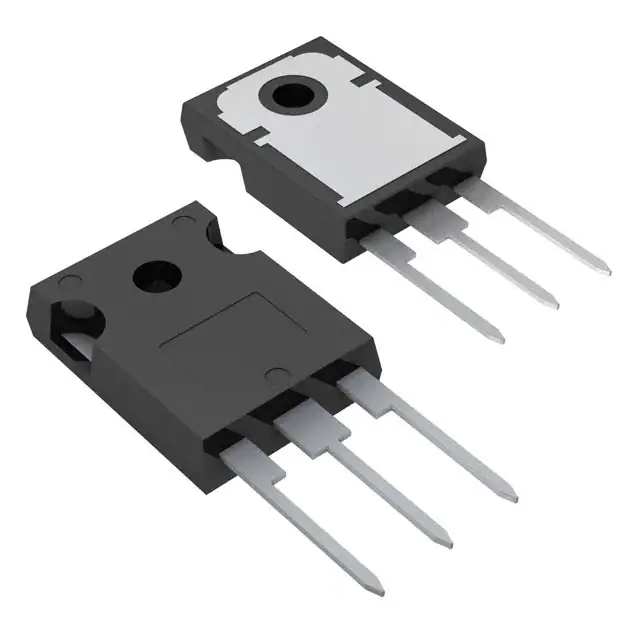
TO-247
e
t
le
)
s
t(
o
r
P
INTERNAL SCHEMATIC DIAGRAM
o
s
b
O
-
APPLICATIONS
HIGH CURRENT, HIGH SPEED SWITCHING
■ SWITCH MODE POWER SUPPLIES (SMPS)
■ DC-AC CONVERTERS FOR WELDING
EQUIPMENT AND UNINTERRUPTIBLE
POWER SUPPLIES AND MOTOR DRIVE
■
)
s
(
ct
u
d
o
r
P
e
ABSOLUTE MAXIMUM RATINGS
t
e
l
o
Symbol
VDS
s
b
O
V DGR
V GS
Value
Unit
Drain-source Voltage (V GS = 0)
Parameter
500
V
Drain- gate Voltage (R GS = 20 kΩ)
500
V
± 30
V
Gate-source Voltage
o
ID
Drain Current (continuous) at T c = 25 C
ID
Drain Current (continuous) at T c = 100 o C
IDM (•)
P tot
dv/dt( 1 )
T stg
Tj
Drain Current (pulsed)
o
Total Dissipation at T c = 25 C
20
A
12.7
A
80
A
250
W
Derating Factor
2
W/o C
Peak Diode Recovery voltage slope
4
V/ns
Storage Temperature
Max. Operating Junction Temperature
(•) Pulse width limited by safe operating area
October 1999
-65 to 150
o
C
150
o
C
(1) ISD ≤ 20A, di/dt ≤ 200 A/µs, VDD ≤ V(BR)DSS, Tj ≤ TJMAX
1/8
�STW20NB50
THERMAL DATA
R thj-case
R thj-amb
R thc-sink
Tl
Thermal Resistance Junction-case
Max
Thermal Resistance Junction-ambient
Max
Thermal Resistance Case-sink
Typ
Maximum Lead Temperature For Soldering Purpose
o
0.5
30
0.1
300
C/W
oC/W
o
C/W
o
C
Max Value
Unit
20
A
1000
mJ
AVALANCHE CHARACTERISTICS
Symbol
Parameter
IAR
Avalanche Current, Repetitive or Not-Repetitive
(pulse width limited by T j max, δ < 1%)
E AS
Single Pulse Avalanche Energy
(starting T j = 25 o C, I D = I AR , V DD = 50 V)
ELECTRICAL CHARACTERISTICS (Tcase = 25 oC unless otherwise specified)
OFF
Symbol
V (BR)DSS
Parameter
Test Conditions
I D = 250 µA
Drain-source
Breakdown Voltage
Zero Gate Voltage
V DS = Max Rating
Drain Current (V GS = 0) V DS = Max Rating
IGSS
Gate-body Leakage
Current (V DS = 0)
Parameter
I D = 250 µA
Gate Threshold
Voltage
V DS = V GS
R DS(on)
Static Drain-source On
Resistance
V GS = 10 V
d
o
r
P
e
bs
O
2/8
C iss
C oss
C rss
Parameter
V DS > I D(on) x R DS(on)max
Input Capacitance
Output Capacitance
Reverse Transfer
Capacitance
V DS = 25 V
f = 1 MHz
uc
od
I D = 10 A
V GS = 0
Unit
V
10
100
µA
µA
± 100
nA
Typ.
Max.
Unit
3
4
5
V
0.22
0.25
Ω
20
Test Conditions
Forward
Transconductance
)
s
t(
Max.
Min.
I D = 10 A
t
c
u
t
e
l
o
g fs (∗)
(s)
On State Drain Current V DS > I D(on) x R DS(on)max
V GS = 10 V
DYNAMIC
Symbol
o
s
b
O
-
Test Conditions
V GS(th)
I D(on)
r
P
e
t
le
T c = 125 o C
V GS = ± 30 V
ON (∗)
Typ.
500
V GS = 0
I DSS
Symbol
Min.
A
Min.
Typ.
9
13.5
3600
460
55
Max.
Unit
S
4700
600
75
pF
pF
pF
�STW20NB50
ELECTRICAL CHARACTERISTICS (continued)
SWITCHING ON
Symbol
Typ.
Max.
Unit
t d(on)
tr
Turn-on Time
Rise Time
Parameter
V DD = 250 V ID = 10 A
VGS = 10 V
R G = 4.7 Ω
(see test circuit, figure 3)
Test Conditions
32
15
43
21
ns
ns
Qg
Q gs
Q gd
Total Gate Charge
Gate-Source Charge
Gate-Drain Charge
V DD = 400 V
85
21
37
110
nC
nC
nC
Typ.
Max.
Unit
20
25
47
27
33
62
ns
ns
ns
I D = 20 A
Min.
V GS = 10 V
SWITCHING OFF
Symbol
tr(Voff)
tf
tc
Parameter
Off-voltage Rise Time
Fall Time
Cross-over Time
Test Conditions
Min.
V DD = 400 V ID = 20 A
R G = 4.7 Ω V GS = 10 V
(see test circuit, figure 5)
SOURCE DRAIN DIODE
Symbol
ISD
I SDM (•)
V SD (∗)
t rr
Q rr
I RRM
Parameter
Test Conditions
Min.
Source-drain Current
Source-drain Current
(pulsed)
Forward On Voltage
I SD = 20 A
Reverse Recovery
Time
Reverse Recovery
Charge
Reverse Recovery
Current
I SD = 20 A di/dt = 100 A/µs
V DD = 100 V
T j = 150 o C
(see test circuit, figure 5)
so
(∗) Pulsed: Pulse duration = 300 µs, duty cycle 1.5 %
(•) Pulse width limited by safe operating area
)
s
(
ct
u
d
o
r
P
e
Safe Operating Area
e
t
le
V GS = 0
b
O
-
c
u
d
Typ.
o
r
P
)
s
t(
Max.
Unit
20
80
A
A
1.6
V
700
ns
9
µC
25
A
Thermal Impedance
t
e
l
o
s
b
O
3/8
�STW20NB50
Output Characteristics
Transfer Characteristics
Transconductance
Static Drain-source On Resistance
c
u
d
e
t
le
)
s
(
ct
u
d
o
r
P
e
Gate Charge vs Gate-source Voltage
t
e
l
o
s
b
O
4/8
o
r
P
o
s
b
O
-
Capacitance Variations
)
s
t(
�STW20NB50
Normalized Gate Threshold Voltage vs
Temperature
Normalized On Resistance vs Temperature
Source-drain Diode Forward Characteristics
c
u
d
e
t
le
)
s
(
ct
)
s
t(
o
r
P
o
s
b
O
-
u
d
o
r
P
e
t
e
l
o
s
b
O
5/8
�STW20NB50
Fig. 1: Unclamped Inductive Load Test Circuit
Fig. 2: Unclamped Inductive Waveform
Fig. 3: Switching Times Test Circuits For
Resistive Load
Fig. 4: Gate Charge test Circuit
c
u
d
e
t
le
)
s
(
ct
u
d
o
r
P
e
Fig. 5: Test Circuit For Inductive Load Switching
And Diode Recovery Times
t
e
l
o
s
b
O
6/8
o
s
b
O
-
o
r
P
)
s
t(
�STW20NB50
TO-247 MECHANICAL DATA
mm
DIM.
MIN.
TYP.
inch
MAX.
MIN.
TYP.
MAX.
A
4.7
5.3
0.185
0.209
D
2.2
2.6
0.087
0.102
E
0.4
0.8
0.016
0.031
F
1
1.4
0.039
0.055
F3
2
2.4
0.079
0.094
F4
3
3.4
0.118
0.134
G
10.9
0.429
H
15.3
15.9
0.602
L
19.7
20.3
0.776
L3
14.2
14.8
0.559
L4
34.6
L5
5.5
M
2
uc
d
o
r
1.362
P
e
let
0.779
0.582
0.217
3
)
s
(
ct
)
s
t(
0.626
0.079
0.118
o
s
b
O
-
u
d
o
r
P
e
t
e
l
o
s
b
O
P025P
7/8
�STW20NB50
c
u
d
e
t
le
)
s
(
ct
)
s
t(
o
r
P
o
s
b
O
-
u
d
o
r
P
e
t
e
l
o
s
b
O
Information furnished is believed to be accurate and reliable. However, STMicroelectronics assumes no responsibility for the consequences
of use of such information nor for any infringement of patents or other rights of third parties which may result from its use. No license is
granted by implication or otherwise under any patent or patent rights of STMicroelectronics. Specification mentioned in this publication are
subject to change without notice. This publication supersedes and replaces all information previously supplied. STMicroelectronics products
are not authorized for use as critical components in life support devices or systems without express written approval of STMicroelectronics.
The ST logo is a trademark of STMicroelectronics
© 1999 STMicroelectronics – Printed in Italy – All Rights Reserved
STMicroelectronics GROUP OF COMPANIES
Australia - Brazil - China - Finland - France - Germany - Hong Kong - India - Italy - Japan - Malaysia - Malta - Morocco Singapore - Spain - Sweden - Switzerland - United Kingdom - U.S.A.
8/8
http://www.st.com
.
�
很抱歉,暂时无法提供与“STW20NB50”相匹配的价格&库存,您可以联系我们找货
免费人工找货