N-CHANNEL 500V - 0.07Ω - 45A TO-247 FDmesh™Power MOSFET (With FAST DIODE)
TYPE STW45NM50FD
n n n n n n
STW45NM50FD
VDSS 500V
RDS(on) < 0.1Ω
ID 45 A
TYPICAL RDS(on) = 0.07Ω HIGH dv/dt AND AVALANCHE CAPABILITIES 100% AVALANCHE TESTED LOW INPUT CAPACITANCE AND GATE CHARGE LOW GATE INPUT RESISTANCE TIGHT PROCESS CONTROL AND HIGH MANUFACTURING YIELDS
3 2 1
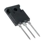
TO-247
DESCRIPTION The FDmesh™ associates all advantages of reduced on-resistance and fast switching with an intrinsic fast-recovery body diode. It is therefore strongly recommended for bridge topologies, in particular ZVS phase-shift converters. APPLICATIONS n ZVS PHASE-SHIFT FULL BRIDGE CONVERTERS FOR SMPS AND WELDING EQUIPMENT
INTERNAL SCHEMATIC DIAGRAM
ABSOLUTE MAXIMUM RATINGS
Symbol VDS VDGR VGS ID ID IDM (l) PTOT dv/dt (1) Tstg Tj Parameter Drain-source Voltage (VGS = 0) Drain-gate Voltage (RGS = 20 kΩ) Gate- source Voltage Drain Current (continuos) at TC = 25°C Drain Current (continuos) at TC = 100°C Drain Current (pulsed) Total Dissipation at TC = 25°C Derating Factor Peak Diode Recovery voltage slope Storage Temperature Max. Operating Junction Temperature Value 500 500 ±30 45 28.4 180 417 2.08 20 –65 to 150 150
(1) ISD ≤45A, di/dt ≤400A/µs, VDD ≤ V (BR)DSS, T j ≤ TJMAX.
Unit V V V A A A W W/°C V/ns °C °C
(•)Pulse width limited by safe operating area
June 2002
1/8
�STW45NM50FD
THERMAL DATA
Rthj-case Rthj-amb Tl Thermal Resistance Junction-case Thermal Resistance Junction-ambient Max Max 0.3 30 300 °C/W °C/W °C
Maximum Lead Temperature For Soldering Purpose
AVALANCHE CHARACTERISTICS
Symbol IAR EAS Parameter Avalanche Current, Repetitive or Not-Repetitive (pulse width limited by Tj max) Single Pulse Avalanche Energy (starting Tj = 25 °C, ID = IAR, VDD = 35 V) Max Value 22.5 800 Unit A mJ
ELECTRICAL CHARACTERISTICS (TCASE = 25 °C UNLESS OTHERWISE SPECIFIED) OFF
Symbol V(BR)DSS IDSS IGSS Parameter Drain-source Breakdown Voltage Zero Gate Voltage Drain Current (VGS = 0) Gate-body Leakage Current (VDS = 0) Test Conditions ID = 250 µA, VGS = 0 VDS = Max Rating VDS = Max Rating, TC = 125 °C VGS = ±30V Min. 500 10 100 ±100 Typ. Max. Unit V µA µA nA
ON (1)
Symbol VGS(th) RDS(on) Parameter Gate Threshold Voltage Static Drain-source On Resistance Test Conditions VDS = VGS, ID = 250µA VGS = 10V, ID = 22.5A Min. 3 Typ. 4 0.07 Max. 5 0.10 Unit V Ω
DYNAMIC
Symbol gfs (1) Ciss Coss Crss Coss eq. (3) RG Parameter Forward Transconductance Input Capacitance Output Capacitance Reverse Transfer Capacitance Equivalent Output Capacitance Gate Input Resistance VGS = 0V, VDS = 0V to 400V f=1 MHz Gate DC Bias = 0 Test Signal Level = 20mV Open Drain Test Conditions VDS > ID(on) x RDS(on)max, ID = 22.5A VDS = 25V, f = 1 MHz, VGS = 0 Min. Typ. 20 3600 680 82 350 2 Max. Unit S pF pF pF pF Ω
Note: 1. Pulsed: Pulse duration = 300 µs, duty cycle 1.5 %.
2/8
�STW45NM50FD
ELECTRICAL CHARACTERISTICS (CONTINUED) SWITCHING ON
Symbol td(on) tr Qg Qgs Qgd Parameter Turn-on Delay Time Rise Time Total Gate Charge Gate-Source Charge Gate-Drain Charge Test Conditions VDD = 250V, ID = 22.5A RG = 4.7Ω VGS = 10V (see test circuit, Figure 3) VDD = 400V, ID = 45A, VGS = 10V Min. Typ. 28 28 92 22 40 120 Max. Unit ns ns nC nC nC
SWITCHING OFF
Symbol tr(Voff) tf tc Parameter Off-voltage Rise Time Fall Time Cross-over Time Test Conditions VDD = 400V, ID = 45A, RG = 4.7Ω, VGS = 10V (see test circuit, Figure 3) Min. Typ. 11 25 44 Max. Unit ns ns ns
SOURCE DRAIN DIODE
Symbol ISD ISDM (2) VSD (1) trr Qrr IRRM Parameter Source-drain Current Source-drain Current (pulsed) Forward On Voltage Reverse Recovery Time Reverse Recovery Charge Reverse Recovery Current ISD = 45A, VGS = 0 ISD = 45A, di/dt = 100A/µs, VDD = 100V (see test circuit, Figure 5) 245 2.2 18 Test Conditions Min. Typ. Max. 45 180 1.5 Unit A A V ns µC A
Note: 1. Pulsed: Pulse duration = 300 µs, duty cycle 1.5 %. 2. Pulse width limited by safe operating area. 3. Coss eq. is defined as a constant equivalent capacitance giving the same charging time as Coss when VDS increases from 0 to 80% VDSS .
Safe Operating Area
Thermal Impedence
3/8
�STW45NM50FD
Output Characteristics Transfer Characteristics
Transconductance
Static Drain-source On Resistance
Gate Charge vs Gate-source Voltage
Capacitance Variations
4/8
�STW45NM50FD
Normalized Gate Thereshold Voltage vs Temp. Normalized On Resistance vs Temperature
Source-drain Diode Forward Characteristics
5/8
�STW45NM50FD
Fig. 1: Unclamped Inductive Load Test Circuit Fig. 2: Unclamped Inductive Waveform
Fig. 3: Switching Times Test Circuit For Resistive Load
Fig. 4: Gate Charge test Circuit
Fig. 5: Test Circuit For Inductive Load Switching And Diode Recovery Times
6/8
�STW45NM50FD
TO-247 MECHANICAL DATA
mm. MIN. 4.85 2.20 0.40 1 3 2 2 3 10.90 15.45 19.85 3.70 18.50 14.20 34.60 5.50 2 5º 60º 3.55 3.65 0.14 3 0.07 5º 60º 0.143 14.80 0.56 1.36 0.21 0.11 15.75 20.15 4.30 0.60 0.78 0.14 0.72 0.58 2.40 3.40 0.07 0.11 0.43 0.62 0.79 0.17 TYP MAX. 5.15 2.60 0.80 1.40 MIN. 0.19 0.08 0.015 0.04 0.11 0.07 0.09 0.13 inch TYP. MAX. 0.20 0.10 0.03 0.05
DIM. A D E F F1 F2 F3 F4 G H L L1 L2 L3 L4 L5 M V V2 Dia
7/8
�STW45NM50FD
Information furnished is believed to be accurate and reliable. However, STMicroelectronics assumes no responsibility for the consequences of use of such information nor for any infringement of patents or other rights of third parties which may result from its use. No license is granted by implication or otherwise under any patent or patent rights of STMicroelectronics. Specification mentioned in this publication are subject to change without notice. This publication supersedes and replaces all information previously supplied. STMicroelectronics products are not authorized for use as critical components in life support devices or systems without express written approval of STMicroelectronics. The ST logo is a trademark of STMicroelectronics © 2000 STMicroelectronics – Printed in Italy – All Rights Reserved STMicroelectronics GROUP OF COMPANIES Australia - Brazil - China - Finland - France - Germany - Hong Kong - India - Italy - Japan - Malaysia - Malta - Morocco Singapore - Spain - Sweden - Switzerland - United Kingdom - U.S.A. http://www.st.com
8/8
�
很抱歉,暂时无法提供与“STW45NM50FD”相匹配的价格&库存,您可以联系我们找货
免费人工找货