STW90NF20
N-channel 200 V, 0.019 Ω, 83 A, TO-247 low gate charge STripFET™ Power MOSFET
Features
Type STW90NF20
■ ■ ■
VDSS 200 V
RDS(on) max < 0.023 Ω
ID 83 A
Exceptional dv/dt capability Low gate charge 100% Avalanche tested
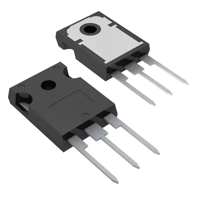
1 2 3
TO-247
Application
■
Switching applications
Description
This Power MOSFET series realized with STMicroelectronics unique STripFET™ process has specifically been designed to minimize input capacitance and gate charge. It is therefore suitable as primary switch in advanced highefficiency isolated DC-DC converters Figure 1. Internal schematic diagram
Table 1.
Device summary
Order code STW90NF20 Marking 90NF20 Package TO-247 Packaging Tube
August 2008
Rev 2
1/12
www.st.com 12
�Contents
STW90NF20
Contents
1 2 Electrical ratings . . . . . . . . . . . . . . . . . . . . . . . . . . . . . . . . . . . . . . . . . . . . 3 Electrical characteristics . . . . . . . . . . . . . . . . . . . . . . . . . . . . . . . . . . . . . 4
2.1 Electrical characteristics (curves) ............................. 6
3 4 5
Test circuits
.............................................. 8
Package mechanical data . . . . . . . . . . . . . . . . . . . . . . . . . . . . . . . . . . . . . 9 Revision history . . . . . . . . . . . . . . . . . . . . . . . . . . . . . . . . . . . . . . . . . . . 11
2/12
�STW90NF20
Electrical ratings
1
Electrical ratings
Table 1.
Symbol VDS VGS ID ID IDM
(1)
Absolute maximum ratings
Parameter Drain-source voltage (VGS = 0) Gate-source voltage Drain current (continuous) at TC = 25 °C Drain current (continuous) at TC = 100 °C Drain current (pulsed) Derating factor Value 200 ± 20 83 52 332 2.4 300 15 -50 to 150 Unit V V A A A W/°C W V/ns °C
PTOT dv/dt (2) TJ Tstg
Total dissipation at TC = 25 °C Peak diode recovery voltage slope Operating junction temperature Storage temperature
1. Pulse width limited by safe operating area 2. ISD ≤ 83 A, di/dt ≤ 400 A/µs, VDD ≤ 80% V(BR)DSS
Table 2.
Symbol Rthj-case Rthj-amb Tl
Thermal resistance
Parameter Thermal resistance junction-case max Thermal resistance junction-ambient max Maximum lead temperature for soldering purpose Value 0.42 50 300 Unit °C/W °C/W °C
Table 3.
Symbol IAR EAS
Avalanche characteristics
Parameter Avalanche current, repetitive or not-repetitive (pulse width limited by TJ max) Single pulse avalanche energy (starting TJ = 25 °C, ID = IAR, VDD = 50 V) Max value 83 400 Unit A mJ
3/12
�Electrical characteristics
STW90NF20
2
Electrical characteristics
(TCASE = 25 °C unless otherwise specified) Table 4.
Symbol V(BR)DSS IDSS IGSS VGS(th) RDS(on)
On/off states
Parameter Drain-source breakdown voltage Zero gate voltage drain current (VGS = 0) Gate body leakage current (VDS = 0) Gate threshold voltage Static drain-source on resistance Test conditions ID = 1 mA, VGS = 0 VDS = Max rating, VDS = Max rating @125 °C VDS = ± 20 V VDS = VGS, ID = 250 µA VGS= 10 V, ID= 45 A 2 3 0.018 Min. 200 1 10 ±100 4 0.023 Typ. Max. Unit V µA µA nA V Ω
Table 5.
Symbol gfs(1) Ciss Coss Crss Coss eq.(2) RG Qg Qgs Qgd
Dynamic
Parameter Forward transconductance Input capacitance Output capacitance Reverse Transfer Capacitance Equivalent output capacitance Intrinsic gate resistance Total gate charge Gate-source charge Gate-drain charge Test conditions VDS = 15 V, ID = 45 A VDS = 25 V, f = 1 MHz, VGS = 0 Min. Typ. 40 5736 1126 196 687 1.7 164 46 72 Max. Unit S pF pF pF pF Ω nC nC nC
VDS = 0 to 160 V, VGS = 0 f = 1 MHz open drain VDD = 160 V, ID = 83 A, VGS = 10 V (see Figure 15)
1. Pulsed: pulse duration = 300µs, duty cycle 1.5% 2. Coss eq. is defined as a constant equivalent capacitance giving the same charging time as Coss when VDS increases from 0 to 80% VDSS
4/12
�STW90NF20 Table 6.
Symbol td(on) tr td(off) tf
Electrical characteristics Switching times
Parameter Turn-on delay time Rise time Turn-off delay time Fall time Test conditions VDD = 100 V, ID = 41.5 A RG = 4.7 Ω, VGS = 10 V, (see Figure 14) Min. Typ. 24 138 148 142 Max. Unit ns ns ns ns
Table 7.
Symbol ISD ISDM(1) VSD(2) trr Qrr IRRM trr Qrr IRRM
Source drain diode
Parameter Source-drain current Source-drain current (pulsed) Forward on voltage Reverse recovery time Reverse recovery charge Reverse recovery current Reverse recovery time Reverse recovery charge Reverse recovery current ISD = 83 A, VGS = 0 ISD = 83 A,VDD = 100 V di/dt = 100 A/µs (see Figure 19) ISD =83 A, VDD = 100 V di/dt = 100 A/µs Tj = 150°C (see Figure 19) 200 1.6 16 235 2.2 18 Test conditions Min. Typ. Max. Unit 83 332 1.6 A A V ns µC A ns µC A
1. Pulse with limited by maximum temperature 2. Pulsed: pulse duration = 300µs, duty cycle 1.5%
5/12
�Electrical characteristics
STW90NF20
2.1
Figure 2.
ID(A)
Electrical characteristics (curves)
Safe operating area
AM00876v1
Figure 3.
Thermal impedance
10µs
(o n
100
Op e Lim rat ite ion d in by th m is a ax re RD a i s S
)
100µs
10
1ms 10ms
1 0.1
1
10
100
VDS(V)
Figure 4.
Output characteristics
AM00877v1
Figure 5.
ID(A) 250
Transfer characteristics
AM00878v1
ID (A) VGS=10V 250 7V 200 6V 150 100 5V 50 4V 0 0 10 20
200 150 100
50 VDS(V) 0 VDS(V)
0
2
4
6
8
10
Figure 6.
BVDSS (norm) 1.10 1.05 1.00 0.95 0.90 0.85 0.8
Normalized BVDSS vs temperature
AM00879v1
Figure 7.
RDS(on) (Ω) 0.0178
Static drain-source on resistance
AM00880v1
ID=1mA VGS=0
ID=45A VGS=0
0.0174
0.0170
0.0166
-50
0
0.0162 50 100 TJ(°C) 5
10
15
20 25 30 35
40
ID(A)
6/12
�STW90NF20 Figure 8.
VGS (V) VDD=160V ID=83A VGS=10V
Electrical characteristics Gate charge vs gate-source voltage Figure 9.
AM00881v1
Capacitance variations
AM00882v1
C (pF) 10000 Ciss 1000
10 8 6 4 2 0 0
Coss Crss
100
50
100
150
200 Qg(nC)
10 0.1
1
10
100
VDS(V)
Figure 10. Normalized gate threshold voltage vs temperature
VGS(th) (norm) 1.1 1.0 0.9
AM00883v1
Figure 11. Normalized on resistance vs temperature
RDS(on) (norm) 2.5 2.0 1.5
AM00884v1
ID=250µA VGS=VDS
0.8 0.7 0.6 0.5 -50 1.0 0.5 0 0 50 100 TJ(°C) -50 0 50 100 TJ(°C)
Figure 12. Source-drain diode forward characteristics
VSD (V) 1.0
Tj=-50°C
AM00885v1
Figure 13. Maximum avalanche energy vs temperature
EAS (mJ) 400 350 300 250
AM00886v1
0.9 0.8 0.7 0.6 0.5 0 0
Tj=150°C Tj=25°C
200 150 100 50 30 50 70 ISD(A) 0 0 10 30 50 70 90 110 130 TJ(°C)
10
7/12
�Test circuits
STW90NF20
3
Test circuits
Figure 15. Gate charge test circuit
Figure 14. Switching times test circuit for resistive load
Figure 16. Test circuit for inductive load Figure 17. Unclamped inductive load test switching and diode recovery times circuit
Figure 18. Unclamped inductive waveform
Figure 19. Switching time waveform
8/12
�STW90NF20
Package mechanical data
4
Package mechanical data
In order to meet environmental requirements, ST offers these devices in ECOPACK® packages. These packages have a Lead-free second level interconnect. The category of second level interconnect is marked on the package and on the inner box label, in compliance with JEDEC Standard JESD97. The maximum ratings related to soldering conditions are also marked on the inner box label. ECOPACK is an ST trademark. ECOPACK specifications are available at: www.st.com
9/12
�Package mechanical data
STW90NF20
TO-247 Mechanical data
mm. Min. 4.85 2.20 1.0 2.0 3.0 0.40 19.85 15.45 5.45 14.20 3.70 18.50 3.55 4.50 5.50 3.65 5.50 14.80 4.30 Typ Max. 5.15 2.60 1.40 2.40 3.40 0.80 20.15 15.75
Dim. A A1 b b1 b2 c D E e L L1 L2 øP øR S
10/12
�STW90NF20
Revision history
5
Revision history
Table 8.
Date 28-Aug-2007 04-Aug-2008
Document revision history
Revision 1 2 First release Document status promoted from preliminary data to datasheet. Changes
11/12
�STW90NF20
Please Read Carefully:
Information in this document is provided solely in connection with ST products. STMicroelectronics NV and its subsidiaries (“ST”) reserve the right to make changes, corrections, modifications or improvements, to this document, and the products and services described herein at any time, without notice. All ST products are sold pursuant to ST’s terms and conditions of sale. Purchasers are solely responsible for the choice, selection and use of the ST products and services described herein, and ST assumes no liability whatsoever relating to the choice, selection or use of the ST products and services described herein. No license, express or implied, by estoppel or otherwise, to any intellectual property rights is granted under this document. If any part of this document refers to any third party products or services it shall not be deemed a license grant by ST for the use of such third party products or services, or any intellectual property contained therein or considered as a warranty covering the use in any manner whatsoever of such third party products or services or any intellectual property contained therein.
UNLESS OTHERWISE SET FORTH IN ST’S TERMS AND CONDITIONS OF SALE ST DISCLAIMS ANY EXPRESS OR IMPLIED WARRANTY WITH RESPECT TO THE USE AND/OR SALE OF ST PRODUCTS INCLUDING WITHOUT LIMITATION IMPLIED WARRANTIES OF MERCHANTABILITY, FITNESS FOR A PARTICULAR PURPOSE (AND THEIR EQUIVALENTS UNDER THE LAWS OF ANY JURISDICTION), OR INFRINGEMENT OF ANY PATENT, COPYRIGHT OR OTHER INTELLECTUAL PROPERTY RIGHT. UNLESS EXPRESSLY APPROVED IN WRITING BY AN AUTHORIZED ST REPRESENTATIVE, ST PRODUCTS ARE NOT RECOMMENDED, AUTHORIZED OR WARRANTED FOR USE IN MILITARY, AIR CRAFT, SPACE, LIFE SAVING, OR LIFE SUSTAINING APPLICATIONS, NOR IN PRODUCTS OR SYSTEMS WHERE FAILURE OR MALFUNCTION MAY RESULT IN PERSONAL INJURY, DEATH, OR SEVERE PROPERTY OR ENVIRONMENTAL DAMAGE. ST PRODUCTS WHICH ARE NOT SPECIFIED AS "AUTOMOTIVE GRADE" MAY ONLY BE USED IN AUTOMOTIVE APPLICATIONS AT USER’S OWN RISK.
Resale of ST products with provisions different from the statements and/or technical features set forth in this document shall immediately void any warranty granted by ST for the ST product or service described herein and shall not create or extend in any manner whatsoever, any liability of ST.
ST and the ST logo are trademarks or registered trademarks of ST in various countries. Information in this document supersedes and replaces all information previously supplied. The ST logo is a registered trademark of STMicroelectronics. All other names are the property of their respective owners.
© 2008 STMicroelectronics - All rights reserved STMicroelectronics group of companies Australia - Belgium - Brazil - Canada - China - Czech Republic - Finland - France - Germany - Hong Kong - India - Israel - Italy - Japan Malaysia - Malta - Morocco - Singapore - Spain - Sweden - Switzerland - United Kingdom - United States of America www.st.com
12/12
�