STX616
High voltage NPN power transistor
Features
■ ■ ■
High voltage capability High DC current gain Minimum lot-to-lot spread for reliable operation
Applications
■ ■
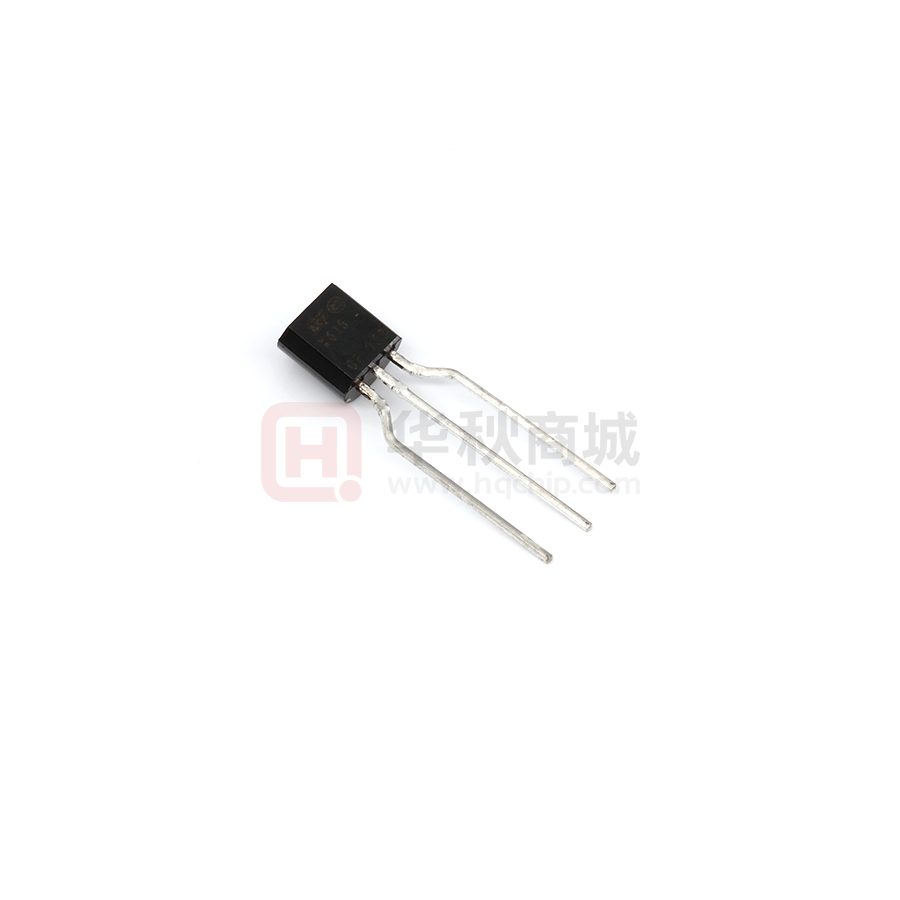
Switching mode power supply Battery charger TO-92 TO-92AP
Description
The device is manufactured using high voltage multi epitaxial planar technology for high switching speeds and high voltage withstand capability. The device is designed for use in SMPS and battery charger.
Figure 1.
Internal schematic diagram
Table 1.
Device summary
Marking X616 X616 Package TO-92 TO-92AP Packaging Bulk Ammopack
Order code STX616 STX616-AP
October 2007
Rev 2
1/8
www.st.com 8
�Electrical characteristics
STX616 STX616-AP
1
Electrical characteristics
(Tcase = 25°C unless otherwise specified) Table 2.
Symbol VCES VCEO VEBO IC ICM IB IBM Ptot Tstg TJ
Absolute maximum rating
Parameter Collector-emitter voltage (V BE = 0) Collector-emitter voltage (IB = 0) Emitter-base voltage (IC = 0) Collector current Collector peak current (tP < 5ms) Base current Base peak current (tP < 5ms) Total dissipation at Tc = 25°C Storage temperature Max. operating junction temperature Value 980 500 12 1.5 2.4 0.8 1.2 2.8 -65 to 150 150 Unit V V V A A A A W °C °C
Table 3.
Symbol Rthj-case Rthj-amb
Thermal data
Parameter Thermal resistance junction-case Thermal resistance junction-ambient __max __max Value 44.6 150 Unit °C/W °C/W
2/8
�STX616 STX616-AP
Electrical characteristics
2
Electrical characteristics
(Tcase = 25°C unless otherwise specified) Table 4.
Symbol ICES
Electrical characteristics
Parameter Collector cut-off current (VBE =0) Collector-emitter sustaining voltage (IB = 0) Emitter-base voltage (IC = 0) Collector-emitter saturation voltage Base-emitter saturation voltage Test conditions VCE = 980V VCE = 980V IC = 10mA Tc = 125°C 500 Min. Typ. Max. 50 0.5 Unit µA mA
VCE(sus) (1)
V
VEBO VCE(sat) (1)
IE = 1mA IC = 0.2A IC = 1A IC = 0.2A IC = 1A IC = 500µA IB = 40mA IB = 200mA IB = 40mA IB = 200mA VCE = 2V V CE = 5V V CE = 5V VCE = 5V
12 0.5 1 1 1.4 17 25 12 4
V V V V V
VBE(sat) (1)
hFE (1)
DC current gain
IC = 200mA IC = 500mA IC = 1.5A
ton ts tf ton ts tf ts tf ts tf
RESISTIVE LOAD Turn-on time Storage time Fall time RESISTIVE LOAD Turn-on time Storage time Fall time INDUCTIVE LOAD Storage time Fall time INDUCTIVE LOAD Storage time Fall time
VCC = 250V IB1 = 65mA
IC = 250mA IB2 = -130mA
0.2 5 0.65
µs µs µs µs µs µs µs µs µs µs
VCC = 250V
IC = 0.8A
1 2.5 0.35
IB1 = 160mA IB2 = -0.4A
Vcl = 300V IB1 = 65mA L = 200µH Vcl = 300V IB1 = 160mA L = 200µH
IC = 250mA IB2 = -130mA IC = 0.8A IB2 = -0.4A 2.5 0.25 5 0.5
Note (1) Pulsed duration = 300 µs, duty cycle ≤ 1.5%
3/8
�Package mechanical data
STX616 STX616-AP
3
Package mechanical data
In order to meet environmental requirements, ST offers these devices in ECOPACK® packages. These packages have a Lead-free second level interconnect. The category of second level interconnect is marked on the package and on the inner box label, in compliance with JEDEC Standard JESD97. The maximum ratings related to soldering conditions are also marked on the inner box label. ECOPACK is an ST trademark. ECOPACK specifications are available at: www.st.com
4/8
�STX616 STX616-AP
Package mechanical data
TO-92 BULK SHIPMENT MECHANICAL DATA
DIM.
mm. MIN. 4.32 0.36 4.45 3.30 2.41 1.14 12.70 2.16 0.92 0.41 5O TYP MAX. 4.95 0.51 4.95 3.94 2.67 1.40 15.49 2.41 1.52 0.56
A b D E e e1 L R S1 W V
0102782 C
5/8
�Package mechanical data
STX616 STX616-AP
TO-92 AMMOPACK SHIPMENT (Suffix”-AP”) MECHANICAL DATA
mm. TYP
DIM. A1 T T1 T2 d P0 P2 F1,F2 delta H W W0 W1 W2 H H0 H1 D0 t L I1 delta P
MIN.
12.50 5.65 2.44 -2.00 17.50 5.70 8.50 18.50 15.50 3.80
12.70 6.35 2.54 18.00 6.00 9.00
16.00 4.00
MAX. 4.80 3.80 1.60 2.30 0.48 12.90 7.05 2.94 2.00 19.00 6.30 9.25 0.50 20.50 16.50 25.00 4.20 0.90 11.00 1.00
3.00 -1.00
6/8
�STX616 STX616-AP
Revision history
4
Revision history
Table 5.
Date 06-Jun-2007 22-Oct-2007
Document revision history
Revision 1 2 Initial release. Added TO-92AP package. Changes
7/8
�STX616 STX616-AP
Please Read Carefully:
Information in this document is provided solely in connection with ST products. STMicroelectronics NV and its subsidiaries (“ST”) reserve the right to make changes, corrections, modifications or improvements, to this document, and the products and services described herein at any time, without notice. All ST products are sold pursuant to ST’s terms and conditions of sale. Purchasers are solely responsible for the choice, selection and use of the ST products and services described herein, and ST assumes no liability whatsoever relating to the choice, selection or use of the ST products and services described herein. No license, express or implied, by estoppel or otherwise, to any intellectual property rights is granted under this document. If any part of this document refers to any third party products or services it shall not be deemed a license grant by ST for the use of such third party products or services, or any intellectual property contained therein or considered as a warranty covering the use in any manner whatsoever of such third party products or services or any intellectual property contained therein.
UNLESS OTHERWISE SET FORTH IN ST’S TERMS AND CONDITIONS OF SALE ST DISCLAIMS ANY EXPRESS OR IMPLIED WARRANTY WITH RESPECT TO THE USE AND/OR SALE OF ST PRODUCTS INCLUDING WITHOUT LIMITATION IMPLIED WARRANTIES OF MERCHANTABILITY, FITNESS FOR A PARTICULAR PURPOSE (AND THEIR EQUIVALENTS UNDER THE LAWS OF ANY JURISDICTION), OR INFRINGEMENT OF ANY PATENT, COPYRIGHT OR OTHER INTELLECTUAL PROPERTY RIGHT. UNLESS EXPRESSLY APPROVED IN WRITING BY AN AUTHORIZED ST REPRESENTATIVE, ST PRODUCTS ARE NOT RECOMMENDED, AUTHORIZED OR WARRANTED FOR USE IN MILITARY, AIR CRAFT, SPACE, LIFE SAVING, OR LIFE SUSTAINING APPLICATIONS, NOR IN PRODUCTS OR SYSTEMS WHERE FAILURE OR MALFUNCTION MAY RESULT IN PERSONAL INJURY, DEATH, OR SEVERE PROPERTY OR ENVIRONMENTAL DAMAGE. ST PRODUCTS WHICH ARE NOT SPECIFIED AS "AUTOMOTIVE GRADE" MAY ONLY BE USED IN AUTOMOTIVE APPLICATIONS AT USER’S OWN RISK.
Resale of ST products with provisions different from the statements and/or technical features set forth in this document shall immediately void any warranty granted by ST for the ST product or service described herein and shall not create or extend in any manner whatsoever, any liability of ST.
ST and the ST logo are trademarks or registered trademarks of ST in various countries. Information in this document supersedes and replaces all information previously supplied. The ST logo is a registered trademark of STMicroelectronics. All other names are the property of their respective owners.
© 2007 STMicroelectronics - All rights reserved STMicroelectronics group of companies Australia - Belgium - Brazil - Canada - China - Czech Republic - Finland - France - Germany - Hong Kong - India - Israel - Italy - Japan Malaysia - Malta - Morocco - Singapore - Spain - Sweden - Switzerland - United Kingdom - United States of America
8/8
�
很抱歉,暂时无法提供与“STX616-AP”相匹配的价格&库存,您可以联系我们找货
免费人工找货