STY60NK30Z
N-CHANNEL 300V - 0.033Ω - 60A Max247 Zener-Protected SuperMESH™Power MOSFET
TYPE STY60NK30Z
s s s s s s
VDSS 300 V
RDS(on) < 0.045 Ω
ID 60 A
Pw 450 W
TYPICAL RDS(on) = 0.033 Ω EXTREMELY HIGH dv/dt CAPABILITY 100% AVALANCHE TESTED GATE CHARGE MINIMIZED VERY LOW INTRINSIC CAPACITANCES VERY GOOD MANUFACTURING REPEATIBILITY
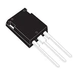
Max247
2 1
3
DESCRIPTION The SuperMESH™ series is obtained through an extreme optimization of ST’s well established stripbased PowerMESH™ layout. In addition to pushing on-resistance significantly down, special care is taken to ensure a very good dv/dt capability for the most demanding applications. Such series complements ST full range of high voltage MOSFETs including revolutionary MDmesh™ products.
INTERNAL SCHEMATIC DIAGRAM
APPLICATIONS s HIGH CURRENT, HIGH EFFICIENCY SWITCHING DC/DC CONVETERS FOR PLASMA TV’s s IDEAL FOR OFF-LINE POWER SUPPLIES, ADAPTORS AND PFC
ORDERING INFORMATION
SALES TYPE STY60NK30Z MARKING Y60NK30Z PACKAGE Max247 PACKAGING TUBE
February 2004
1/8
�STY60NK30Z
ABSOLUTE MAXIMUM RATINGS
Symbol VDS VDGR VGS ID ID IDM ( ) PTOT VESD(G-S) dv/dt (1) Tj Tstg Parameter Drain-source Voltage (VGS = 0) Drain-gate Voltage (RGS = 20 kΩ) Gate- source Voltage Drain Current (continuous) at TC = 25°C Drain Current (continuous) at TC = 100°C Drain Current (pulsed) Total Dissipation at TC = 25°C Derating Factor Gate source ESD(HBM-C=100 pF, R=1.5 KΩ) Peak Diode Recovery voltage slope Operating Junction Temperature Storage Temperature Value 300 300 ± 30 60 37.5 240 450 3.57 6000 4.5 -55 to 150 Unit V V V A A A W W/°C V V/ns °C
( ) Pulse width limited by safe operating area (1) ISD ≤60A, di/dt ≤ 200A/µs, VDD ≤ V(BR)DSS, Tj ≤ T JMAX.
THERMAL DATA
Rthj-case Rthj-amb Tl Thermal Resistance Junction-case Max Thermal Resistance Junction-ambient Max Maximum Lead Temperature For Soldering Purpose 0.28 30 300 °C/W °C/W °C
AVALANCHE CHARACTERISTICS
Symbol IAR EAS Parameter Avalanche Current, Repetitive or Not-Repetitive (pulse width limited by Tj max) Single Pulse Avalanche Energy (starting Tj = 25 °C, ID = IAR, VDD = 50 V) Max Value 60 0.7 Unit A J
GATE-SOURCE ZENER DIODE
Symbol BVGSO Parameter Gate-Source Breakdown Voltage Test Conditions Igs=± 1mA (Open Drain) Min. 30 Typ. Max. Unit V
PROTECTION FEATURES OF GATE-TO-SOURCE ZENER DIODES The built-in back-to-back Zener diodes have specifically been designed to enhance not only the device’s ESD capability, but also to make them safely absorb possible voltage transients that may occasionally be applied from gate to source. In this respect the Zener voltage is appropriate to achieve an efficient and cost-effective intervention to protect the device’s integrity. These integrated Zener diodes thus avoid the usage of external components.
2/8
�STY60NK30Z
ELECTRICAL CHARACTERISTICS (TCASE =25°C UNLESS OTHERWISE SPECIFIED) ON/OFF
Symbol V(BR)DSS IDSS IGSS VGS(th) RDS(on) Parameter Drain-source Breakdown Voltage Zero Gate Voltage Drain Current (VGS = 0) Gate-body Leakage Current (VDS = 0) Gate Threshold Voltage Static Drain-source On Resistance Test Conditions ID = 1 mA, VGS = 0 VDS = Max Rating VDS = Max Rating, TC = 125 °C VGS = ± 20 V VDS = VGS, ID = 100 µA VGS = 10V, ID = 30 A 3 3.75 0.033 Min. 300 1 50 ±10 4.5 0.045 Typ. Max. Unit V µA µA µA V Ω
DYNAMIC
Symbol gfs (1) Ciss Coss Crss Coss eq. (3) Parameter Forward Transconductance Input Capacitance Output Capacitance Reverse Transfer Capacitance Equivalent Output Capacitance Parameter Turn-on Delay Time Rise Time Total Gate Charge Gate-Source Charge Gate-Drain Charge Test Conditions VDS = 15 V, ID = 30 A VDS = 25V, f = 1 MHz, VGS = 0 Min. Typ. 29 7200 1070 250 880 Max. Unit S pF pF pF pF
VGS = 0V, VDS = 0V to 240V
SWITCHING ON
Symbol td(on) tr Qg Qgs Qgd Test Conditions VDD = 150 V, ID = 30 A RG = 4.7Ω , VGS = 10 V (Resistive Load see, Figure 3) VDD = 240 V, ID = 60 A, VGS = 10 V Min. Typ. 50 90 220 46 123 Max. Unit ns ns nC nC nC
SWITCHING OFF
Symbol td(off) tf tr(Voff) tf tc Parameter Turn-off Delay Time Fall Time Off-voltage Rise Time Fall Time Cross-over Time Test Conditions VDD = 150 V, ID = 30 A RG = 4.7Ω , VGS = 10 V (Resistive Load see, Figure 3) VDD = 240 V, ID = 60 A, RG = 4.7Ω, VGS = 10V (Inductive Load see, Figure 5) Min. Typ. 150 60 40 65 110 Max. Unit ns ns ns ns ns
SOURCE DRAIN DIODE
Symbol ISD ISDM (2) VSD (1) trr Qrr IRRM Parameter Source-drain Current Source-drain Current (pulsed) Forward On Voltage Reverse Recovery Time Reverse Recovery Charge Reverse Recovery Current ISD = 60 A, VGS = 0 ISD = 60 A, di/dt = 100 A/µs VR = 100 V, Tj = 150°C (see test circuit, Figure 5) 475 6.4 27 Test Conditions Min. Typ. Max. 60 240 1.6 Unit A A V ns µC A
Note: 1. Pulsed: Pulse duration = 300 µs, duty cycle 1.5 %. 2. Pulse width limited by safe operating area. 3. Coss eq. is defined as a constant equivalent capacitance giving the same charging time as Coss when VDS increases from 0 to 80% VDSS.
3/8
�STY60NK30Z
Safe Operating Area Thermal Impedance
Output Characteristics
Transfer Characteristics
Transconductance
Static Drain-source On Resistance
4/8
�STY60NK30Z
Gate Charge vs Gate-source Voltage Capacitance Variations
Normalized Gate Thereshold Voltage vs Temp.
Normalized On Resistance vs Temperature
Source-drain Diode Forward Characteristics
5/8
�STY60NK30Z
Fig. 1: Unclamped Inductive Load Test Circuit Fig. 2: Unclamped Inductive Waveform
Fig. 3: Switching Times Test Circuit For Resistive Load
Fig. 4: Gate Charge test Circuit
Fig. 5: Test Circuit For Inductive Load Switching And Diode Recovery Times
6/8
�STY60NK30Z
Max247 MECHANICAL DATA
mm MIN. A A1 b b1 b2 c D e E L L1 4.70 2.20 1.00 2.00 3.00 0.40 19.70 5.35 15.30 14.20 3.70 TYP. MAX. 5.30 2.60 1.40 2.40 3.40 0.80 20.30 5.55 15.90 15.20 4.30 MIN. inch TYP. MAX.
DIM.
P025Q
7/8
�STY60NK30Z
Information furnished is believed to be accurate and reliable. However, STMicroelectronics assumes no responsibility for the consequences of use of such information nor for any infringement of patents or other rights of third parties which may result from its use. No license is granted by implication or otherwise under any patent or patent rights of STMicroelectronics. Specifications mentioned in this publication are subject to change without notice. This publication supersedes and replaces all information previously supplied. STMicroelectronics products are not authorized for use as critical components in life support devices or systems without express written approval of STMicroelectronics. The ST logo is a registered trademark of STMicroelectronics All other names are the property of their respective owners © 2004 STMicroelectronics - All Rights Reserved STMicroelectronics GROUP OF COMPANIES Australia - Belgium - Brazil - Canada - China - Czech Republic - Finland - France - Germany - Hong Kong - India - Israel - Italy - Japan Malaysia - Malta - Morocco - Singapore - Spain - Sweden - Switzerland - United Kingdom - United States. http://www.st.com
8/8
�
很抱歉,暂时无法提供与“STY60NK30Z”相匹配的价格&库存,您可以联系我们找货
免费人工找货