T1610T-8G
Datasheet
16 A - 800 V logic level T-series Triac in D²PAK
Features
A2
A2
A1
G
•
•
•
•
150 °C maximum junction temperature
Three quadrants
High commutation on resistive loads
Surge capability VDSM, VRSM = 900 V
•
Benefits:
–
Easy direct control by MCU thanks to low 10 mA IGT
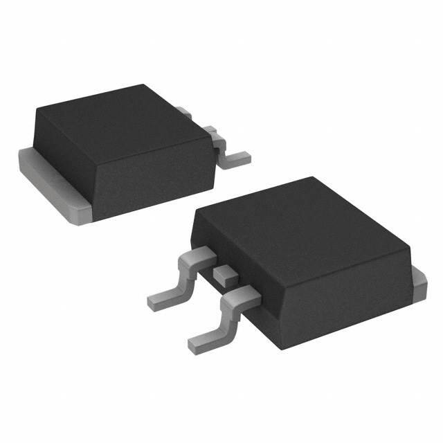
D²PAK
–
A2
A2: Anode2
A1: Anode1
G: Gate
G
A1
Increase of thermal margin due to extended working Tj up to 150 °C
Applications
•
•
•
•
•
General purpose AC line load switching
Small home appliances with resistive loads
Hybrid relays
Inrush current limiting circuits
Overvoltage crowbar protection
Description
The SMD T1610T-8G Triac can be used for the on/off or phase angle control function
in general purpose AC switching with resistive loads. A Logic level T-series Triac, the
T1610T-8G can be controlled directly from an MCU with a simplified circuit. T-series
triacs are optimized for high EMI constraints.
Product status link
T1610T-8G
Product summary
IT(RMS)
16 A
VDRM/VRRM
800 V
VDSM/VRSM
900 V
IGT
10 mA
The surface mount D2PAK package enables compact SMT designs for automated
manufacturing.
D2PAK package's molding compound resin is halogen-free and meets UL94
flammability standard level V0.
Package environmentally friendly Ecopack2 graded (RoHS and Halogen Free
compliance).
DS12532 - Rev 3 - October 2020
For further information contact your local STMicroelectronics sales office.
www.st.com
�T1610T-8G
Characteristics
1
Characteristics
Table 1. Absolute maximum ratings (limiting values), Tj = 25 °C unless otherwise specified
Symbol
Parameter
Value
Unit
Tj = 125 °C
800
V
Tj = 150 °C
600
V
tp = 10 ms, Tj = 25 °C
900
V
RMS on-state current (full sine wave)
Tc = 126 °C
16
A
Non repetitive surge peak on-state current (full cycle, Tj initial = 25
°C
t = 16.7 ms
126
t = 20 ms
120
I2t value for fusing
tp = 10 ms
95
A2s
dl/dt
Critical rate of rise of on-state current, IG = 2 x IGT, tr ≤ 100 ns
f = 100 Hz
100
A/µs
IGM
Peak gate current
4
A
VGM
Peak Gate Voltage
5
V
1
W
Storage junction temperature range
-40 to +150
°C
Operating junction temperature range
-40 to +150
°C
VDRM/VRRM Repetitive peak off-state voltage (50-60 Hz)
VDSM/VRSM Non Repetitive peak off-state voltage
IT(RMS)
ITSM
I2t
PG(AV)
Tstg
Tj
tp = 20 µs, Tj = 150 °C
Tj = 150 °C
Average gate power dissipation
A
Table 2. Electrical characteristics (Tj = 25 °C, unless otherwise specified)
Symbol
Quadrants; Tj
Test conditions
Value
Unit
IGT(1)
VD = 12 V, RL = 30 Ω
I - II - III
Max.
10
mA
VGT
VD = 12 V, RL = 30 Ω
I - II - III
Max.
1.3
V
VGD
VD = 800 V, RL = 3.3 kΩ
I - II - III
Min.
0.2
V
IG = 1.2 x IGT
I - III
Max.
20
mA
IG = 1.2 x IGT
II
Max.
30
mA
Max.
25
mA
IL
IH
(2)
dV/dt (2)
Tj = 125 °C
IT = 500 mA, gate open
VD = 536 V, gate open
Tj = 125 °C
Min.
100
V/µs
VD = 402 V, gate open
Tj = 150 °C
Min.
50
V/µs
(dV/dt)c = 0.1 V/μs
(dl/dt)c (2)
(dV/dt)c = 10 V/μs
Tj = 125 °C
Tj = 150 °C
Tj = 125 °C
Tj = 150 °C
Min.
Min.
9
5.4
3
1.8
A/ms
A/ms
1. Minimum IGT is guaranteed at 5% of IGT max
2. For both polarities of A2 referenced to A1.
DS12532 - Rev 3
page 2/12
�T1610T-8G
Characteristics
Table 3. Static characteristics
Symbol
Tj
Test conditions
Value
Unit
VTM (1)
IT = 22.6 A, tp = 380 µs
25 °C
Max.
1.55
V
VTO(1)
Threshold on-state voltage
150 °C
Max.
0.85
V
RD(1)
Dynamic resistance
150 °C
Max.
34
mΩ
5
µA
1.0
mA
3.6
mA
Value
Unit
Max.
1.15
°C/W
Typ.
45
°C/W
IDRM/IRRM
25 °C
VDRM = VRRM = 800 V
125°C
VDRM = VRRM = 600 V
150 °C
Max.
Max.
1. For both polarities of A2 referenced to A1.
Table 4. Thermal resistance
Symbol
Parameter
Rth(j-c)
Junction to case (AC)
Rth(j-a)
Junction to ambient (SCU (1) = 2 cm2)
D2PAK
1. Scu : copper pad surface under tab, 35 μm copper thickness on FR4 PCB.
DS12532 - Rev 3
page 3/12
�T1610T-8G
Characteristics (curves)
1.1
Characteristics (curves)
Figure 1. Maximum power dissipation versus on-state
RMS current
Figure 2. On-state RMS current versus case temperature
IT(RMS)(A)
P(W)
22
18
20
16
α = 180°
18
14
16
12
14
α = 180°
10
12
8
10
6
8
4
6
4
2
Tc(°C)
2
180°
0
IT(RMS)(A)
0
25
50
75
100
125
150
0
0
2
4
6
8
10
12
14
16
Figure 3. On-state RMS current versus ambient
temperature (free air convection)
IT(RMS)(A)
Figure 4. Relative variation of thermal impedance versus
pulse duration
1.0E+00
4.0
K = [Z th / Rth]
Zth(j-c)
α = 180°
3.5
Zth(j-a)
3.0
2.5
2.0
1.0E-01
1.5
1.0
0.5
Ta(°C)
0.0
0
25
50
75
100
125
150
Figure 5. Relative variation of gate trigger voltage and
current versus junction temperature (typical values)
Tp (s)
1.0E-02
1.0E-03 1.0E-02 1.0E-01 1.0E+00 1.0E+01 1.0E+02 1.0E+03 1.0E+04
Figure 6. Relative variation of holding current and
latching current versus junction temperature (typical
values)
IGT,VGT[Tj] / IGT,VGT[Tj = 25 °C]
IH,IL [Tj] / IH,IL [Tj = 25 °C]
2.0
2.0
3Q IGT Q3
1.5
1.5
1.0
1.0
3Q IGT Q1-Q2
IL
0.5
0.5
IH
Tj (°C)
0.0
-50
DS12532 - Rev 3
-30
-10
10
30
50
70
90
110
130
150
Tj (°C)
0.0
-50
-30
-10
10
30
50
70
90
110
130
150
page 4/12
�T1610T-8G
Characteristics (curves)
Figure 7. Surge peak on-state current versus number of
cycles
Figure 8. Non repetitive surge peak on-state current for a
sinusoidal pulse with width tp < 10 ms
ITSM(A)
ITSM(A)
10000
130
Tj initial=25°C
120
110
t=20ms
100
90
80
dI/dt limitation:
100A/µs
One cy cle
Non repetitive
Tj initial = 25 °C
1000
70
ITSM
60
Repetitive
Tc = 126°C
50
40
100
30
20
10
Number of cycles
0
1
10
t p (ms)
10
100
0.01
1000
Figure 9. Relative variation of critical rate of decrease of
main current versus junction temperature (typical values)
0.10
1.00
10.00
Figure 10. Relative variation of critical rate of decrease of
main voltage versus junction temperature
dV/dt [Tj] / dV/dt [Tj = 150 °C]
(dI/dt)c [Tj] / (dI/dt)c [Tj = 150 °C]
4
10
VD = VR = 536 V
9
8
3
7
6
2
5
4
3
1
2
Tj(°C)
Tj(°C)
1
0
0
25
50
75
100
125
150
Figure 11. On-state characteristics (maximum values)
ITM(A)
1000
25
50
75
100
125
Figure 12. Relative variation of leakage current versus
junction temperature for different values of blocking
voltage
IDRM/IRRM [Tj, VDRM/VRRM] / IDRM/IRRM [Tj max.,VDRM/VRRM]*
Tj max.
Vto = 0.85 V
Rd = 34 mΩ
1.0E+00
*[Tj max = 125 °C; VDRM, VRRM = 800 V]
[Tj max = 150 °C; VDRM, VRRM = 600 V]
Tj = 25 °C
100
1.0E-01
VDRM = VRRM = 600 V
Tj = 150 °C
10
VDRM = VRRM = 800 V
1.0E-02
VDRM = VRRM = 400 V
1.0E-03
VTM(V)
1
0
1
2
3
4
5
Tj(°C)
1.0E-04
25
DS12532 - Rev 3
50
75
100
125
150
page 5/12
�T1610T-8G
Characteristics (curves)
Figure 13. Thermal resistance junction to ambient versus copper surface under tab
Rth(j-a) (°C/W)
80
Epoxy printed circuit board FR4, eCu = 35 µm
D²PAK
70
60
50
40
30
20
SCu (cm²)
10
0
0
DS12532 - Rev 3
5
10
15
20
25
30
35
40
page 6/12
�T1610T-8G
Package information
2
Package information
In order to meet environmental requirements, ST offers these devices in different grades of ECOPACK packages,
depending on their level of environmental compliance. ECOPACK specifications, grade definitions and product
status are available at: www.st.com. ECOPACK is an ST trademark.
2.1
D²PAK package information
•
•
•
ECOPACK2 compliant
Lead-free package leads finishing
Molding compound resin is halogen-free and meets UL standard level V0
Figure 14. D²PAK package outline
A
E
E1
E2
H
D
D1
L2
c2
2
3
D2
L3
1
b2
b
e
Max resin gate protrusion: 0.5 mm (1)
G
A1
A2
A3
L
R
Gauge Plane
V2
c
(1) Resin gate is accepted in each of position shown on the drawing, or their symmetrical.
DS12532 - Rev 3
page 7/12
�T1610T-8G
D²PAK package information
Table 5. D²PAK package mechanical data
Dimensions
Inches(1)
Millimeters
Ref.
Min.
Typ.
Max.
Min.
Typ.
Max.
A
4.30
4.60
0.1693
0.1811
A1
2.49
2.69
0.0980
0.1059
A2
0.03
0.23
0.0012
A3
0.25
0.0091
0.0098
b
0.70
0.93
0.0276
0.0366
b2
1.25
1.7
0.0492
0.0669
c
0.45
0.60
0.0177
0.0236
c2
1.21
1.36
0.0476
0.0535
D
8.95
9.35
0.3524
0.3681
D1
7.50
8.00
0.2953
0.3150
D2
1.30
1.70
0.0512
0.0669
e
2.54
0.1
E
10.00
10.28
0.3937
0.4047
E1
8.30
8.70
0.3268
0.3425
E2
6.85
7.25
0.2697
0.2854
G
4.88
5.28
0.1921
0.2079
H
15
15.85
0.5906
0.6240
L
1.78
2.28
0.0701
0.0898
L2
1.19
1.40
0.0468
0.0551
L3
1.40
1.75
0.0551
0.0689
R
V2(2)
0.40
0°
0.0157
8°
0°
8°
1. Dimensions in inches are given for reference only
2. Degrees
DS12532 - Rev 3
page 8/12
�T1610T-8G
D²PAK package information
Figure 15. D²PAK recommended footprint (dimensions are in mm)
16.90
10.30
5.08
1.30
8.90
3.70
Figure 16. D²PAK stencil definitions(dimensions are in mm)
DS12532 - Rev 3
page 9/12
�T1610T-8G
Ordering information
3
Ordering information
Figure 17. Ordering information scheme
T 16
10
T -
8
G
TR
Series
T = T-series Triac
Current (RMS) / Type
16 = 16 A
Gate Current
10 = 10 mA
Specific application
T = T-series Triac
Voltage
8 = 800 V
Package
G = D²PAK
Packing
Blank = Tube
TR = Tape and reel
Table 6. Ordering information
Order code
T1610T-8G-TR
T1610T-8G
DS12532 - Rev 3
Marking
Package
Weight
T1610T-8G
D²PAK
1.6 g
Base qty.
Delivery mode
1000
Tape and reel
50
Tube
page 10/12
�T1610T-8G
Revision history
Table 7. Document revision history
Date
Version
Changes
03-Apr-2018
1
Initial release.
17-Jul-2018
2
Updated Table 2. Electrical characteristics (Tj = 25 °C, unless otherwise
specified).
29-Oct-2020
3
Updated Table 5 and added Figure 13. Thermal resistance junction to ambient
versus copper surface under tab.
Minor text changes.
DS12532 - Rev 3
page 11/12
�T1610T-8G
IMPORTANT NOTICE – PLEASE READ CAREFULLY
STMicroelectronics NV and its subsidiaries (“ST”) reserve the right to make changes, corrections, enhancements, modifications, and improvements to ST
products and/or to this document at any time without notice. Purchasers should obtain the latest relevant information on ST products before placing orders. ST
products are sold pursuant to ST’s terms and conditions of sale in place at the time of order acknowledgement.
Purchasers are solely responsible for the choice, selection, and use of ST products and ST assumes no liability for application assistance or the design of
Purchasers’ products.
No license, express or implied, to any intellectual property right is granted by ST herein.
Resale of ST products with provisions different from the information set forth herein shall void any warranty granted by ST for such product.
ST and the ST logo are trademarks of ST. For additional information about ST trademarks, please refer to www.st.com/trademarks. All other product or service
names are the property of their respective owners.
Information in this document supersedes and replaces information previously supplied in any prior versions of this document.
© 2020 STMicroelectronics – All rights reserved
DS12532 - Rev 3
page 12/12
�
很抱歉,暂时无法提供与“T1610T-8G-TR”相匹配的价格&库存,您可以联系我们找货
免费人工找货- 国内价格
- 1+12.04200
- 10+11.77200
- 30+11.58840
- 国内价格 香港价格
- 1000+3.647151000+0.46782
- 国内价格 香港价格
- 1+15.004101+1.92458
- 10+9.5152710+1.22053
- 100+6.35061100+0.81460
- 500+4.99264500+0.64041
- 国内价格 香港价格
- 1000+4.555791000+0.58438
- 2000+4.188262000+0.53723
- 3000+4.000993000+0.51321
- 5000+3.790575000+0.48622
- 7000+3.666007000+0.47024
- 10000+3.5449410000+0.45471
- 国内价格 香港价格
- 2000+2.921732000+0.37477
- 3000+2.866853000+0.36773
- 5000+2.781955000+0.35684
- 7000+2.729637000+0.35013
- 10000+2.7090510000+0.34749
- 国内价格 香港价格
- 1000+3.497391000+0.44861
- 国内价格 香港价格
- 1+13.942401+1.78840
- 10+8.8517010+1.13550
- 100+5.90520100+0.75750
- 500+4.64750500+0.59620
- 1000+4.228201000+0.54240
- 2000+3.844902000+0.49320
- 国内价格 香港价格
- 1000+2.964611000+0.38027
- 2000+2.934592000+0.37642
- 3000+2.905443000+0.37268
- 5000+2.884855000+0.37004
- 7000+2.841127000+0.36443
- 10000+2.7948110000+0.35849
- 国内价格 香港价格
- 2000+2.921732000+0.37477
- 3000+2.917443000+0.37422
- 5000+2.858275000+0.36663
- 7000+2.805967000+0.35992
- 10000+2.7536510000+0.35321
- 国内价格 香港价格
- 1000+2.975761000+0.38170
- 2000+2.945742000+0.37785
- 3000+2.916583000+0.37411
- 5000+2.896005000+0.37147
- 7000+2.852277000+0.36586
- 10000+2.8051010000+0.35981