T4050-6PF
Datasheet
40 A Snubberless™ Triac
Features
A2
G
A1
•
•
•
High current Triac
High surge current = 400 A
Max. blocking voltage = VDRM, VRRM = 600 V
•
Max. surge voltage = VDSM, VRSM = 700 V
•
IGT maximum = 50 mA
•
•
•
High static and dynamic commutation:
–
(dI/dt)c = 25.1 A/ms
–
dV/dt = 1000 V/μs
UL1557 certified (file ref. 81734) = 2.5 kV
Snubberless™ device
•
ECOPACK®2 compliant (RoHS and HF compliance)
G
A2
A1
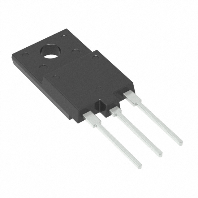
TO-3PF
Applications
•
•
•
•
Product status link
T4050-6PF
Product summary
IT(RMS)
40 A
VDRM, VRRM
600 V
VDSM, VRSM
700 V
IGT
50 mA
Heater, ventilation and air conditioning (HVAC)
Solid state relay (SSR)
Motor soft starter
SMPS inrush current limiter
Description
The device is packaged in a through-hole TO-3PF full plastic insulated.
The T4050-6PF is optimized for the ON/OFF function or phase angle control in
applications such as static relays, heating regulation, induction motor starting circuits,
light dimmers, motor speed controllers and in many other industrial applications
where high immunity and high surge current are required.
DS12857 - Rev 1 - December 2018
For further information contact your local STMicroelectronics sales office.
www.st.com
�T4050-6PF
Characteristics
1
Characteristics
Table 1. Absolute maximum ratings (limiting values)
Symbol
IT(RMS)
ITSM
I2t
dl/dt
Parameter
Unit
A
RMS on-state current (full sine wave)
Tc = 76 °C
40
Non repetitive surge peak on-state current
t = 16.7 ms
420
(full cycle,Tj initial = 25 °C)
t = 20 ms
400
I2t value for fusing
tp = 10 ms
1000
A2s
50
A/µs
600
V
700
V
8
A
8
V
1
W
2.5
kV
Critical rate of rise of on-state current,
IG = 2 x IGT, tr ≤ 100 ns
VDRM/VRRM
Repetitive peak off-state voltage (50-60 Hz)
VDSM/VRSM
Non repetitive peak off-state voltage
IGM
Peak gate current
VGM
Peak gate voltage
PG(AV)
Value
Average gate power dissipation
F = 120 Hz, Tj = 25 °C
tp = 10 ms, Tj = 25 °C
tp = 20 µs, Tj = 125 °C
Tj = 125 °C
A
Vins.
Insulation RMS voltage, 1 minute (UL1557 file E81734)
Tstg
Storage temperature range
-40 to +150
°C
Tj
Operating junction temperature range
-40 to +125
°C
TL
Maximum lead temperature for soldering during 10 s
260
°C
Table 2. Electrical characteristics (Tj = 25 °C, unless otherwise specified)
Symbol
IGT(1)
VGT
VGD
IL
IH
(2)
dV/dt (2)
(dl/dt)c (2)
Test conditions
VD = 12 V, RL = 33 Ω
VD = 600 V, RL = 3.3 kΩ
IG = 1.2 x IGT
Quadrants; Tj
Value
Unit
Max.
50
mA
Max.
1.3
V
Min.
0.2
V
I - III
Max.
70
mA
II
Max.
160
mA
Max.
85
mA
I - II - III
I - II - III
Tj = 125 °C
IT = 500 mA, gate open
VD = 402 V, gate open
Tj = 125 °C
Min.
1000
V/µs
Snubberless™ (dV/dt)c > 20 V/μs
Tj = 125 °C
Min.
25.1
A/ms
1. Minimum IGT is guaranteed at 5% of IGT max
2. For both polarities of A2 referenced to A1.
DS12857 - Rev 1
page 2/11
�T4050-6PF
Characteristics
Table 3. Static electrical characteristics
Symbol
VTM(1)
Tj
Test conditions
Value
Unit
ITM = 60 A, tp = 380 µs
25 °C
Max.
1.4
V
VTO
Threshold voltage
125 °C
Max.
0.85
V
RD(1)
Dynamic resistance
125 °C
Max.
10
mΩ
5
µA
7.5
mA
Value
Unit
(1)
IDRM/IRRM
25 °C
VDRM = VRRM = 600 V
125°C
Max.
1. For both polarities of A2 referenced to A1.
Table 4. Thermal resistance
Symbol
DS12857 - Rev 1
Parameter
Rth(j-c)
Junction to case (AC)
Rth(j-a)
Junction to ambient
Max.
1.45
Typ.
1.1
Typ.
50
°C/W
page 3/11
�T4050-6PF
Characteristics (curves)
1.1
Characteristics (curves)
Figure 1. Maximum power dissipation versus on-state
RMS current
P(W)
48
Figure 2. On-state RMS current versus case temperature
44
44
40
40
36
36
32
32
28
28
24
24
20
20
16
16
12
12
IT(RMS)(A)
8
180°
8
4
4
IT(RMS)(A)
TC(°C)
0
0
0
0
4
8
12
16
20
24
28
32
36
Figure 3. On-state RMS current versus ambient
temperature (free air convection)
3.5
25
50
75
100
125
40
IT(RMS)(A)
Figure 4. Relative variation of thermal impedance versus
pulse duration
1.0E+00
K=[Z th /Rth ]
Zth(j-c)
3.0
Zth(j-a)
2.5
2.0
1.0E-01
1.5
1.0
0.5
Ta(°C)
0.0
0
DS12857 - Rev 1
25
50
75
100
125
1.0E-02
t P(s)
1.0E-03 1.0E-02 1.0E-01 1.0E+00 1.0E+01 1.0E+02 1.0E+03 1.0E+04 1.0E+05
page 4/11
�T4050-6PF
Characteristics (curves)
Figure 5. Relative variation of gate trigger voltage and
current versus junction temperature (typical values)
Figure 6. Relative variation of holding current and
latching current versus junction temperature (typical
values)
IGT, VGT[T j] / I GT, VGT[T j= 25 °C]
2.0
1.5
IH, IL [T j] / I H, IL [T j = 25 °C]
IGT Q3
1.5
IGT Q1-Q2
1.0
IL
1.0
VGT Q1-Q2-Q3
0.5
0.5
IH
Tj(°C)
Tj(°C)
0.0
-50
-25
0
25
50
75
100
Figure 7. Relative variation of static dV/dt immunity
versus junction temperature
6
0.0
125
dV/dt [Tj ] / dV/dt [Tj = 125 °C]
-50
0
25
50
75
100
125
Figure 8. Relative variation of critical rate of decrease of
main current versus junction temperature
7
VD = VR = 402 V
-25
(dI/dt) c [T j] / (dI/dt) c [T j = 125 °C]
6
5
5
4
4
3
3
2
2
1
1
Tj(°C)
0
25
50
75
100
125
Figure 9. Surge peak on-state current versus number of
cycles
450
ITSM(A)
Tj(°C)
0
25
50
75
100
Figure 10. Non repetitive surge peak on-state current for a
sinusoidal pulse with width tp < 10 ms
10000
ITSM(A)
Tj initial = 25 °C
dI/dt limitation: 50 A/µs
400
350
125
t=20ms
One cycle
Non repetitive
Tj initial = 25 °C
300
1000
250
200
150
100
100
Repetitive
TC = 76 °C
50
t P(ms)
Number of cycles
0
10
1
DS12857 - Rev 1
10
100
1000
0.01
0.10
1.00
10.00
page 5/11
�T4050-6PF
Characteristics (curves)
Figure 11. On-state characteristics (maximum values)
1000
Figure 12. Relative variation of Leakage current versus
junction temperature
ITM (A)
1.0E+00
IDRM/IRRM[Tj] / IDRM/IRRM[Tj = 125 °C]
1.0E-01
100
VDRM=VRRM = 600 V
Tj = 125 °C
1.0E-02
Tj = 25 °C
10
1.0E-03
Tj max :
Vto = 0.85 V
Rd = 10 mΩ
VTM (V)
Tj(°C)
1
0
DS12857 - Rev 1
1
2
3
4
5
1.0E-04
25
50
75
100
125
page 6/11
�T4050-6PF
Package information
2
Package information
In order to meet environmental requirements, ST offers these devices in different grades of ECOPACK®
packages, depending on their level of environmental compliance. ECOPACK® specifications, grade definitions
and product status are available at: www.st.com. ECOPACK® is an ST trademark.
2.1
TO-3PF package information
•
•
•
Epoxy meets UL94, V0
Lead-free package and HF package
Recommended torque: 0.8N·m (max. 1.0 N·m)
Figure 13. TO-3PF package outline
A
H
C
DIA
L5
L
L2
L3
L6
L4
N
F2(3X)
D1
D
R
L7
F(3X)
E
G1
G
Projection
DS12857 - Rev 1
page 7/11
�T4050-6PF
TO-3PF package information
Table 5. TO-3PF mechanical data
Dimensions
Ref.
Inches(1)
mm
Min.
Typ.
Max.
Min.
Typ.
Max.
A
5.30
5.70
0.2087
0.2244
C
2.80
3.20
0.1102
0.1260
D
3.10
3.50
0.1220
0.1378
D1
1.80
2.20
0.0709
0.0866
E
0.80
1.10
0.0315
0.0433
F
0.65
0.95
0.0256
0.0374
F2
1.80
2.20
0.0709
0.0866
G
10.30
11.50
0.4055
0.4528
G1
5.45
H
15.30
L
9.80
L2
0.2146
15.70
0.6024
10.20
0.3858
22.80
23.20
0.8976
0.9134
L3
26.30
26.70
1.0354
0.0512
L4
43.20
44.40
1.7008
1.7480
L5
4.30
4.70
0.1693
0.1850
L6
24.30
24.70
0.9567
0.9724
L7
14.60
15.00
0.5748
0.5906
N
1.80
2.20
0.0709
0.0866
R
3.80
4.20
0.1496
0.1654
Dia
3.40
3.80
0.1339
0.1496
10.00
0.6181
0.3937
0.4016
1. Inches given for reference only
DS12857 - Rev 1
page 8/11
�T4050-6PF
Ordering information
3
Ordering information
Figure 14. Ordering information scheme
T
40
50
-
6
PF
SnubberlessTM Triac
Current (RMS) / type
40 = 40 A
Gate current
50 = 50 mA
Voltage
6 = 600 V
Package
PF = TO-3PF
Table 6. Ordering information
DS12857 - Rev 1
Order code
Marking
Package
Weight
Base qty.
Delivery mode
T4050-6PF
T4050-6PF
TO-3PF
5.2 g
30
Tube
page 9/11
�T4050-6PF
Revision history
Table 7. Document revision history
DS12857 - Rev 1
Date
Version
03-Dec-2018
1
Changes
Initial release.
page 10/11
�T4050-6PF
IMPORTANT NOTICE – PLEASE READ CAREFULLY
STMicroelectronics NV and its subsidiaries (“ST”) reserve the right to make changes, corrections, enhancements, modifications, and improvements to ST
products and/or to this document at any time without notice. Purchasers should obtain the latest relevant information on ST products before placing orders. ST
products are sold pursuant to ST’s terms and conditions of sale in place at the time of order acknowledgement.
Purchasers are solely responsible for the choice, selection, and use of ST products and ST assumes no liability for application assistance or the design of
Purchasers’ products.
No license, express or implied, to any intellectual property right is granted by ST herein.
Resale of ST products with provisions different from the information set forth herein shall void any warranty granted by ST for such product.
ST and the ST logo are trademarks of ST. All other product or service names are the property of their respective owners.
Information in this document supersedes and replaces information previously supplied in any prior versions of this document.
© 2018 STMicroelectronics – All rights reserved
DS12857 - Rev 1
page 11/11
�
很抱歉,暂时无法提供与“T4050-6PF”相匹配的价格&库存,您可以联系我们找货
免费人工找货- 国内价格
- 1+17.82000
- 10+15.36700
- 300+14.91600
- 国内价格
- 10+65.35250
- 100+38.98500
- 200+27.28950
- 300+19.49250
- 600+18.51790
- 3000+17.15340
- 国内价格
- 1+24.41880
- 10+20.71440
- 30+18.51120
- 国内价格 香港价格
- 1+39.278961+4.91451
- 30+21.7152430+2.71697
- 120+17.83753120+2.23180
- 510+14.99303510+1.87590
- 1020+13.954661020+1.74598
- 2010+13.638512010+1.70643
- 国内价格 香港价格
- 1+29.442601+3.68380
- 3+27.907253+3.49170
- 10+24.5656110+3.07360
- 30+20.6820730+2.58770
- 150+20.50144150+2.56510


 工商网监
湘ICP备2023018690号
工商网监
湘ICP备2023018690号
