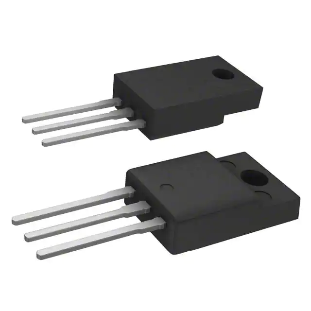
T610T-8FP
6 A logic level Triac
Datasheet − production data
$�
Description
$�
Available in through-hole fullpack package, the
T610T-8FP Triac can be used for the on/off or
phase angle control function in general purpose
AC switching. This device can be directly driven
by a microcontroller thanks to its 10 mA gate
current requirement. Provide UL certified
insulation rated at 2000 VRMS.
*
$�
Table 1. Device summary
*
72����)3$%
$�
$�
Symbol
Value
Unit
IT(rms)
6
A
VDRM, VRRM
800
V
VDSM, VRSM
900
V
IGT
10
mA
Features
• Medium current Triac
• Three triggering quadrants Triac
• ECOPACK®2 compliant component
• Complies with UL standards (File ref: E81734)
• 6 A high performance Triac:
– High Tj family
– High dI/dt family
– High dV/dt family
• Insulated package TO-220FPAB:
– Insulated voltage: 2000 VRMS
Applications
• General purpose AC line load switching
• Motor control circuits
• Small home appliances
• Lighting
• Inrush current limiting circuits
• Overvoltage crowbar protection
February 2015
This is information on a product in full production.
DocID025568 Rev 2
1/9
www.st.com
9
�Characteristics
1
T610T-8FP
Characteristics
Table 2. Absolute maximum ratings (Tj = 25 °C unless otherwise stated)
Symbol
IT(rms)
ITSM
I ²t
Parameter
A
Tc = 117 °C
6
Non repetitive surge peak on-state F = 50 Hz
current (full cycle, Tj initial = 25 °C) F = 60 Hz
t = 20 ms
45
t = 16.7 ms
47
I²t value for fusing, Tj initial = 25 °C
tp = 10 ms
13
Tj = 150 °C
600
Tj = 125 °C
800
tp = 10 ms
900
V
100
A/µs
Tj = 150 °C
4
A
Tj = 150 °C
1
W
- 40 to + 150
- 40 to + 150
°C
260
°C
2
kV
Repetitive surge peak off-state voltage
VDSM,
VRSM
Non repetitive surge peak off-state voltage
dI/dt
Critical rate of rise of on-state
current IG = 2 x IGT, tr ≤ 100 ns
F = 100 Hz
IGM
Peak gate current
tp = 20 µs
Average gate power dissipation
A
Tstg
Tj
Storage junction temperature range
Operating junction temperature range
TL
Maximum lead temperature for soldering during 10 s
Vins
Unit
On-state rms current (full sine wave)
VDRM,
VRRM
PG(AV)
Value
Insulation rms voltage, 1 minute
A ²s
V
Table 3. Electrical characteristics (Tj = 25 °C, unless otherwise stated)
Symbol
Test conditions
Quadrant
0.5
Max.
10
I - II - III
Max.
1.3
V
I - II - III
Min.
0.2
V
Max.
15
mA
I - III
Max.
20
mA
II
Max.
25
mA
250
V/µs
170
V/µs
VD = 12 V, RL = 30 Ω
I - II - III
VGT
VD = 12 V, RL = 30 Ω
VGD
VD = VDRM, RL = 3.3 k Ω , Tj = 150 °C
IH (1)
IT = 500 mA
IL
IG = 1.2 IGT
(dI/dt)c (1)
VD = VR = 536 V, gate open
Tj = 125 °C
VD = VR = 402 V, gate open
Tj = 150 °C
Tj = 125 °C
(dV/dt)c = 0.1 V/µs
mA
Min.
5.2
Min.
Tj = 150 °C
(dI/dt)c (1)
Tj = 125 °C
(dV/dt)c = 10 V/µs
Tj = 150 °C
1. For both polarities of A2 referenced to A1
2/9
DocID025568 Rev 2
Unit
Min.
IGT
dV/dt (1)
Value
A/ms
3.7
2.7
Min.
A/ms
1.2
�T610T-8FP
Characteristics
Table 4. Static characteristics
Symbol
Test conditions
VT (1)
Value
Unit
ITM = 8.5 A, tp = 380 µs
Tj = 25 °C
Max.
1.55
V
Vt0
(1)
Threshold voltage
Tj = 150 °C
Max.
0.85
V
Rd
(1)
Dynamic resistance
Tj = 150 °C
Max.
75
mΩ
5
µA
Tj = 25 °C
VDRM = VRRM = 800 V
IDRM
IRRM
Max.
Tj = 125 °C
VDRM = VRRM = 600 V
0.6
mA
Tj = 150 °C
Max.
2.0
1. For both polarities of A2 referenced to A1
Table 5. Thermal resistance
Symbol
Parameter
Value
Unit
Rth(j-c)
Junction to case (AC)
4.5
°C/W
Rth(j-a)
Junction to ambient (DC)
60
°C/W
Figure 1. Maximum power dissipation versus
on-state rms current (full cycle)
8
Figure 2. On-state rms current versus case
temperature (full cycle)
P(W)
7
� =180
IT(RMS)(A)
� =180°
6
6
5
4
4
3
2
2
180°
�
IT(RMS)(A)
0
0
1
2
3
1
�
4
6
Figure 3. On-state rms current versus ambient
temperature (free air convection)
3.0
TC(°C)
0
5
IT(RMS)(A)
0
25
50
100
125
150
Figure 4. Relative variation of thermal
impedance versus pulse duration
1.0E+00
K = [Zth / Rth]
� =180°
2.5
75
Zth(j-c)
Zth(j-a)
2.0
1.0E-01
1.5
1.0
0.5
tp (s)
Ta(°C)
0.0
0
25
50
75
100
125
150
1.0E-02
1.0E-03
DocID025568 Rev 2
1.0E-02
1.0E-01
1.0E+00
1.0E+01
1.0E+02
1.0E+03
3/9
�Characteristics
T610T-8FP
Figure 5. On-state characteristics (maximum
values)
100
ITM(A)
ITSM(A)
50
45
40
35
30
25
20
15
10 Repetitive
5 TC= 117 °C
0
Tj max :
Vto = 0.85 V
Rd = 75 mΩ
10
Tj = 150 °C
T j = 25 °C
VTM(V)
1
0.0
0.5
1.0
1.5
2.0
2.5
3.0
3.5
4.0
Figure 7. Non repetitive surge peak on-state
current and corresponding values of I2t
1000
Figure 6. Surge peak on-state current versus
number of cycles
t = 20 ms
Non repetitive
Tj initial=25°C
One cycle
Number of cycles
1
10
100
1000
Figure 8. Relative variation of gate trigger
current and gate voltage versus junction
temperature (typical values)
ITSM(A), I²t (A²s)
I GT, VGT [ Tj ] / I GT ,V GT [ T j = 25 °C ]
Tj initial = 25 °C
dI/dt limitation: 100 A/µs
2.5
IGT Q1-Q2
2.0
ITSM
1.5
100
1.0
Half cycle sinusoidal pulse with
width tp < 10 ms
10
0.01
0.10
VGT
0.5
I²t
tp(ms)
1.00
10.00
Figure 9. Relative variation of static dV/dt
immunity versus junction temperature (typical
values)
5
IGT Q3
0.0
-50
Tj(°C)
-25
25
50
75
100
125
150
Figure 10. Relative variation of holding current
and latching current versus junction
temperature (typical values)
I , I [T j ] / I H , I L [T j = 25 °C ]
2.0 H L
dV/dt [Tj ] / dV/dt [Tj =150 °C]
VD = V R = 402 V ; 150°C
VD = VR = 536 V ; 125°C
4
0
IH
1.5
IL
3
1.0
2
0.5
1
0
25
4/9
Tj(°C)
50
75
100
125
Tj(°C)
0.0
150
-50
DocID025568 Rev 2
-25
0
25
50
75
100
125
150
�T610T-8FP
Characteristics
Figure 11. Relative variation of critical rate of
decrease of main current (dI/dt)c versus
reapplied (dV/dt)c (typical values)
3
Figure 12. Relative variation of critical rate of
decrease of main current (dI/dt)c versus
junction temperature (typical values)
(dI/dt)c [ (dV/dt)c ] / Specified (dI/dt)c
8
(dI/dt)C [T j] / (dI/dt)c [T j=150 °C]
(dV/dt)c = 10 V/µs
7
Tj = 150 ° C
6
2
5
4
1
3
Tj = 125 ° C
2
1
(dV/dt)c (V/µs)
0
0.1
1.0
10.0
Tj(°C)
0
25
100.0
50
75
100
125
150
Figure 13. Relative variation of leakage current versus junction temperature for
different values of blocking voltage (typical values)
IDRM, IRRM [Tj;V DRM, V RRM] / IDRM, IRRM
1.0E+00
V DRM = V RRM = 800 V
1.0E-01
V DRM = V RRM = 600 V
1.0E-02
V DRM = V RRM = 400 V
1.0E-03
[Tj = 125 °C; 800 V] ;
[Tj = 150°C; 600 V]
Tj(°C)
1.0E-04
25
50
75
100
DocID025568 Rev 2
125
150
5/9
�Package information
2
T610T-8FP
Package information
•
Epoxy meets UL94, V0
•
Lead-free package
•
Recommended torque: 0.4 to 0.6 N·m
In order to meet environmental requirements, ST offers these devices in different grades of
ECOPACK® packages, depending on their level of environmental compliance. ECOPACK®
specifications, grade definitions and product status are available at: www.st.com.
ECOPACK® is an ST trademark.
Figure 14. TO-220FPAB dimension definitions
A
B
H
Dia
L6
L2
L7
L3
L5
F1
L4
F2
F
G1
G
6/9
D
DocID025568 Rev 2
E
�T610T-8FP
Package information
Table 6. TO-220FPAB dimensions
Dimensions
Ref.
Millimeters
Inches
Min.
Max.
Min.
Max.
A
4.4
4.6
0.173
0.181
B
2.5
2.7
0.098
0.106
D
2.5
2.75
0.098
0.108
E
0.45
0.70
0.018
0.027
F
0.75
1
0.030
0.039
F1
1.15
1.70
0.045
0.067
F2
1.15
1.70
0.045
0.067
G
4.95
5.20
0.195
0.205
G1
2.4
2.7
0.094
0.106
H
10
10.4
0.393
0.409
L2
16 Typ.
0.63 Typ.
L3
28.6
30.6
1.126
1.205
L4
9.8
10.6
0.386
0.417
L5
2.9
3.6
0.114
0.142
L6
15.9
16.4
0.626
0.646
L7
9.00
9.30
0.354
0.366
Dia.
3.00
3.20
0.118
0.126
DocID025568 Rev 2
7/9
�Ordering information
3
T610T-8FP
Ordering information
Figure 15. Ordering information scheme
T
6
10
T -
8
FP
Triac
Current
6=6A
Gate sensitivity
10 = 10 mA
Specific application
T = Increased (dI/dt)c and dV/dt producing reduced ITSM
Voltage (VDRM, VRRM)
8 = 800 V
Package
FP = TO-220FPAB
Table 7. Ordering information
4
Order code
Marking
Package
Weight
Base qty
Delivery mode
T610T-8FP
T610T-8FP
TO-220FPAB
2.0 g
50
Tube
Revision history
Table 8. Document revision history
8/9
Date
Revision
Changes
05-Feb-2014
1
Initial release.
12-Feb-2015
2
Updated Features and Table 2.
DocID025568 Rev 2
�T610T-8FP
IMPORTANT NOTICE – PLEASE READ CAREFULLY
STMicroelectronics NV and its subsidiaries (“ST”) reserve the right to make changes, corrections, enhancements, modifications, and
improvements to ST products and/or to this document at any time without notice. Purchasers should obtain the latest relevant information on
ST products before placing orders. ST products are sold pursuant to ST’s terms and conditions of sale in place at the time of order
acknowledgement.
Purchasers are solely responsible for the choice, selection, and use of ST products and ST assumes no liability for application assistance or
the design of Purchasers’ products.
No license, express or implied, to any intellectual property right is granted by ST herein.
Resale of ST products with provisions different from the information set forth herein shall void any warranty granted by ST for such product.
ST and the ST logo are trademarks of ST. All other product or service names are the property of their respective owners.
Information in this document supersedes and replaces information previously supplied in any prior versions of this document.
© 2015 STMicroelectronics – All rights reserved
DocID025568 Rev 2
9/9
�
很抱歉,暂时无法提供与“T610T-8FP”相匹配的价格&库存,您可以联系我们找货
免费人工找货- 国内价格 香港价格
- 1000+6.075061000+0.78424
- 国内价格
- 1+18.13810
- 10+12.09210
- 30+10.07680
- 国内价格
- 1+17.05320
- 10+14.29920
- 30+12.58200