TD310
TRIPLE IGBT/MOS DRIVER WITH CURRENT SENSE
■ THREE POWER IGBT/MOS AND PULSE
TRANSFORMER DRIVERS
■ CURRENT SENSE COMPARATOR
■ UNCOMMITTED OP-AMP
■ 0.6 A PER CHANNEL PEAK OUTPUT
CURRENT CAPABILITY
■ LOW OUTPUT IMPEDANCE TYP: 7Ω AT
N
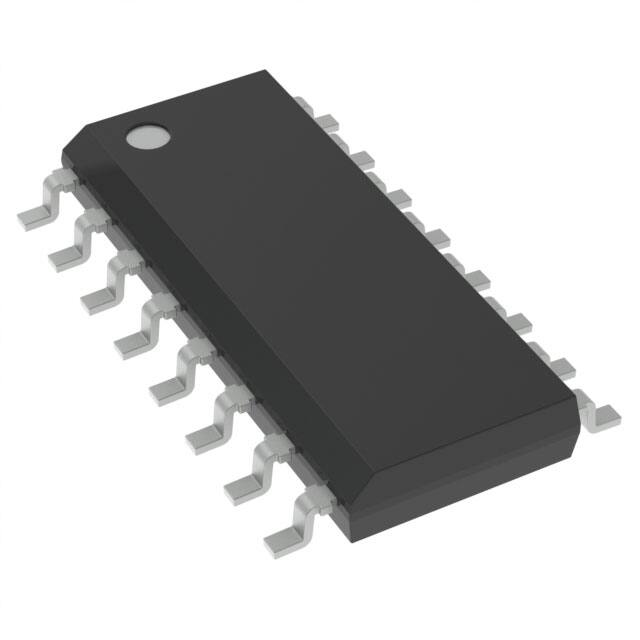
DIP-16
(Plastic Package)
200mA
■ CMOS/LSTTL COMPATIBLE INVERTING
INPUT WITH HYSTERESIS
■ 4V TO 16V SINGLE SUPPLY OPERATION
■ LOW BIAS CURRENT TYP: 1.5mA
■ ADJUSTABLE UNDERVOLTAGE LOCKOUT
D
SO-16
(Plastic Micropackage)
LEVEL
■ STAND-BY MODE
■ CHANNEL PARALLELING CAPABILITY
ORDER CODE
DESCRIPTION
The TD310 is designed to drive one, two or three
Power IGBT/MOS and has driving capability for
pulse transformer. So it is perfectly suited to
interface control IC with Power Switches in low
side or half-bridge configuration.
TD310 includes a current sense comparator which
inhibit the output drivers in case of overcurrent. An
alarm output signals the even to a controller.
TD310 also includes an uncommitted op-amp
which can be used for current measurement (as
an amplifier before the A/D input of a
microcontroller) of for other general purpose.
Programmable undervoltage lockout and standby
mode make TD310 suitable for a large area of
environment and application.
Typical applications are low side IGBT and power
MOSFET drive in three phase systems, pulse
transformer drive, and general purpose pulse
drive.
December 2001
Part Number
Temperature Range
TD310I
-40°C, +125°C
Package
N
D
•
•
N = Dual in Line Package (DIP)
D = Small Outline Package (SO) - also available in Tape & Reel (DT)
PIN CONNECTIONS (top view)
VCC
1
16
UVLO/Stby
INA
2
15
OUTA
INB
3
14
OUTB
INC
4
13
OUTC
Enable
5
12
Gnd
Alarm
6
11
Sense -
OA Output
7
10
OA Input -
OA Input +
8
9
Sense +
1/9
�TD310
BLOCK DIAGRAM
VCC
Standby
Standby
VCC
Stby
1.26M
0.7V
UVLO
TD310
140k
GND
1.2V
INA
OUTA
INB
OUTB
INC
OUTC
Enable
Control
Sense+
Unit
Alarm
Sense OA output
OA input +
GND
OA InputGND
ABSOLUTE MAXIMUM RATINGS
Symbol
VCC
Parameter
Supply Voltage
Value
Unit
18
0 to VCC
V
V
Vi
Input Voltage
Vis
Sense Input Voltage
-0.3 to VCC
V
Tj
Operating Junction Temperature
-40 to 150
°C
Tamb
Operating Ambient Temperature
-40 to 125
°C
Value
Unit
4 to 16
V
OPERATING CONDITIONS
Symbol
VCC
Parameter
Supply Voltage
INSTRUCTION FOR USE
1 - The TD310 supply voltage must be decoupled with a 1µF min. capacitor.
2 - If the application involving TD310 requires maximum output current capability, this current must be
pulsed: pulse width 1µsec, duty cycle 1% at Tamb.
2/9
�TD310
ELECTRICAL CHARACTERISTICS
VCC = 15V, Tamb = 25°C (unless otherwise specified)
Symbol
ICC
Parameter
Min.
Supply Current with Inputs in High State
Typ.
Max.
Unit
1.5
2
mA
LOGIC INPUT (all inputs)
VIH
VIL
IIH
IIL
tdH, teL
tdL, teH
tli
tdd
High Input Voltage
Low Input Voltage
High Input Current
Low Input Current
Propagation Delay (10% input to 10% output)
Output Delay
Output Delay
Tmin. ≤ Tamb ≤ Tmax.
2
0.8
10
10
200
60
Input Inhibiting Time
Differential Delay Time Between Channels
400
400
100
20
V
V
pA
pA
ns
ns
ns
OUTPUT DRIVERS
Vsod
Vsid
Vdem
Ropd
Sourcing Drop Voltage (A/B/C outputs)
Isource = 200mA
Sinking Drop Voltage (A/B/C outputs)
Isink = 200mA
Demagnetizing Drop Voltage (A/B/C outputs)
Idemag. = 100mA
Output Pull Down Resistor
3
V
5
V
2
V
47
kΩ
35
mA
ALARM OUTPUT
Is
Low Level Sinking Current
VO = 0.8V
Ish
tA
High Level Sinking Current
Alarm Output : Delay Time to Alarm Fall if Sense Input Triggered
5
1
500
µA
ns
20
mV
ms
600
ns
SENSE INPUT
Vios
tAi
ts
tsi
Vshys
Input Offset Voltage
Inhibition Time if Sense Input Triggered
Delay Time to Output Fall if Sense Input Triggered
All outputs inhibited
Inhibition Time of Sense Input
Sense Hysteresis
1
300
40
ns
mV
OPERATIONAL AMPLIFIER
Vicm
Common Mode Input Voltage Range
Vio
GBP
Avd
Input Offset Voltage
Gain Bandwidth Product
Open Loop Gain
Slew Rate at Unity Gain (RL = 100kΩ, CL = 100pF, Vi = 3 to 7V)
SR
0 to VCC+ - 1.5
V
10
mV
MHz
dB
V/µs
1.1
V
µA
1
60
0.6
STAND-BY
Vstdby
Istdby
Standby Mode Threshold Voltage
Standby Mode Supply Current
0.3
30
UNDER VOLTAGE LOCKOUT
Iadj
Vst1
Vhys
Under Voltage Level Adjust Current
Internal Stop Threshold (without external adjustment)
Threshold Hysteresis
1
10.7
13.3
0.8
µA/V
V
V
3/9
�TD310
UVLO/stdby pin functioning modes
Due to the wide supply voltage range of the TD310, the UVLO function (Under Voltage Lock Out) is
externally adjustable by a resistor bridge.
The bridge rate can be calculated in relation with the expected UVLO protection level as follows :
R1
R1 + R2
VUVLO x ---------------------
= 1.2V (where R1 is the lower resistor of the bridge)
The internal resistor sets the default UVLO value to 12V (*) and might influence the external bridge rate if
the values of the external resistors are too high. Moreover, the internal resistor ratio is accurate, but the
the tolerance on the absolute value of each internal resistor (typically 140k and 1.26M) is about +/-20%.
If an external bridge is used, we recommend to choose resistor values not greater than 10k.
The standby threshold value depends of the UVLO value as follows:
Vstdby = 0.7/1.2 VUVLO
Both UVLO and stdby functions can be inhibited by connecting the UVLO/stdby pin to VCC+ via a pull up
resistor (ex 150kΩ).
The following table summarizes the functions of the TD310 :
Pin
16
9/11
5
2/3/4
15/14/13
6
7/8/10
Config
UVLO/
stdby
Sense+/
Sense-
Enable
In A/B/C
Out A/B/C
Alarm
Op-Amp
L
1
H
+>Normal
Stdby
2
L
UVLO
3
M
++
很抱歉,暂时无法提供与“TD310IDT”相匹配的价格&库存,您可以联系我们找货
免费人工找货- 国内价格
- 1+24.57678
- 8+16.24844
- 21+15.35028
- 国内价格 香港价格
- 1+24.016581+3.09620
- 10+17.7056610+2.28260
- 25+16.6538325+2.14700
- 100+15.77732100+2.03400
- 250+15.16375250+1.95490