TDA7467
AUDIO MATRIX WITH SRS EFFECTS
The Device incorporates the SRS
(Sound Retrieval System) under
licence from SRS Labs, Inc.
■
■
■
■
■
■
■
1 STEREO INPUT
INPUT ATTENUATION CONTROL IN 0.5dB
STEP
– MUTE FUNCTION
MONO MODE (SRS 3D MONO)
STEREO MODE (SRS 3D STEREO)
SPACE AND CENTER ATTENUATORS ARE
AVAILABLE
ALL FUNCTION ARE PROGRAMMABLE VIA
SERIAL BUS (I2C BUS)
c
u
d
)
s
t(
nents and it is not affected by internal process
spreads.
o
r
P
The AC signal setting is obtained by resistor networks and switches combined with operational
amplifiers according to the SRS labs specification.
DESCRIPTION
The TDA7467 is a SRS (Sound Retrieval System)
audio matrix. It reproduces SRS sound processing
stereo and mono sources both.
PIN CONNECTION (Top view)
RIN
)
s
(
ct
2
27
CREF
LIN
3
26
LP2
DIG_GND
4
25
LP1
SCL
5
24
HP6
ADDR
6
23
HP5
SDA
7
22
HP4
AGND
8
21
VS
PS1
9
20
HP3
PS2
10
19
HP2
PS3
11
18
HP1
PS4
12
17
VREFOUT
PS5
13
16
NETW2
PS6
14
15
NETW1
LOUT
o
r
P
e
t
e
l
o
e
t
le
Control of all the functions is accomplished by serial bus. Thanks to the used BIPOLAR/CMOS/
DMOS technology, Low Distortion, Low Noise and
DC stepping are obtained.
o
s
b
O
-
The SRS sound is guaranteed by external compo-
s
b
O
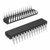
DIP28
SO28
ORDERING NUMBERS:
TDA7467
TDA7467D
du
1
28
ROUT
D96AU507
November 2003
1/11
�L-IN
R-IN
0.15µF
0.15µF
2
3
50K
50K
21
31.5dB
control
VS
31.5dB control
8
27
SUPPLY
-
+
22µF
17
SRS
12
PS4
CREF
PS5
PS6
14
VREF
4.42K
15
MONO
10
9
1.5K
0.47µF
1K
NETW1
3.74K
47.5K
NETW2
-
+
4.7nF
SPACE
MIX
MIX
+
22
20
0.1µF
HPF1
19
18
1µF
c
u
d
0.47µF
32.4K
130K
16
11
PS3
PHASE SHIFTER 1
PS2
PS1
CENTER
PHASE SHIFTER 2
13
0.47nF
HP1
4.7nF
HP2
27nF
HP3
2.2nF
HP4
15nF
)
s
(
ct
o
s
b
O
-
AGND
r
P
e
u
d
o
e
t
le
VREFOUT
HPF2
24
0.1µF
23
1µF
HP5
2/11
HP6
s
b
O
t
e
l
o
100nF
25
1µF
LPF1
26
LP1
+
+
SRS
FIX
MONO
FIX
SRS
MONO
+
2
4
6
7
5
1
D96AU506
I2C BUS DECODER + LATCHES
+
LP2
0.1µF
R-OUT
DIG_GND
ADDR
SDA
SCL
L-OUT
TDA7467
BLOCK DIAGRAM
)
s
t(
o
r
P
�TDA7467
THERMAL DATA
Symbol
Rth j-pins
Parameter
Thermal Resistance Junction-pins
Value
Unit
85
°C/W
Value
Unit
11
V
-10 to 85
°C
-55 to +150
°C
Max.
ABSOLUTE MAXIMUM RATINGS
Symbol
VS
Parameter
Operating Supply Voltage
Tamb
Operating Ambient Temperature
Tstg
Storage Temperature Range
QUICK REFERENCE DATA
Symbol
VS
Parameter
Supply Voltage
VCL
Max. input signal handling
THD
Total Harmonic Distortion V = 1Vrms f = 1KHz
S/N
Signal to Noise Ratio Vout = 1Vrms (mode = OFF)
SC
Channel Separation f = 1KHz
Typ.
Max.
Unit
7
9
10.2
V
uc
2
d
o
r
0.01
P
e
let
SRS Center Control (1dB step)
so
SRS Space Control (1dB step)
Mute Attenuation
)
s
(
ct
0.1
106
Input Control (0.5dB)
)
s
t(
Min.
Vrms
%
dB
90
dB
-31.5
0
dB
-31
0
dB
0
dB
-31
b
O
-
100
dB
ELECTRICAL CHARACTERISTCS
Refer to the test circuit Tamb = 25°C, VS = 9V, RL = 10KΩ, Vin = 1Vrms; RG = 600Ω, all controls flat
(G = 0dB), Effect Ctrl = -6dB, MODE = OFF; f = 1KHz unless otherwise specified
Symbol
u
d
o
Parameter
r
P
e
SUPPLY
VS
Supply Voltage
IS
Supply Current
t
e
l
o
SVR
Ripple Rejection
Test Condition
LCH / RCH out, Mode = OFF
Min.
Typ.
Max.
Unit
7
9
10.2
V
60
25
mA
80
dB
INPUT STAGE
s
b
O
RIN
VCL
Input Resistance
Clipping Level
THD = 0.3%
37.5
50
2
2.5
62.5
KΩ
Vrms
AVMIN
Min. Attenuation
-1
0
1
AVMAX
Max. Attenuation
31
31.5
32
dB
ASTEP
Step Resolution
-1
0.5
1
dB
-3
0
3
mV
0
dB
VDC
DC Steps
Adjacent att. step
dB
SRS EFFECT CONTROL
Crange1
Sstep1
Center/Space Control Range
Center/Space Step Resolution
-31
1
dB
3/11
�TDA7467
ELECTRICAL CHARACTERISTCS (continued)
Refer to the test circuit Tamb = 25°C, VS = 9V, RL = 10KΩ, Vin = 1Vrms; RG = 600Ω, all controls flat
(G = 0dB), Effect Ctrl = -6dB, MODE = OFF; f = 1KHz unless otherwise specified
Symbol
Parameter
Test Condition
Min.
Typ.
Max.
Unit
AUDIO OUTPUTS
N
o(Off)
Output Noise (OFF)
Output muted, Flat
BW (20Hz to 20KHz)
4
5
µVrms
µVrms
N
o(srs)
Output noise (srs)
Surround Sound
BW (20Hz to 20KHz)
50
µVrms
Distortion
AV = 0; Vin = 1Vrms
0.01
d
SC
Channel Separation
0.1
%
90
dB
Vocl
Clipping Level
2.5
Vrms
Rout
Output Resistance
30
Ω
Vout
DC Voltage Level
3.8
V
d = 0.3%
2
BUS INPUTS
Vil
Input Low Voltage
Vih
Input High Voltage
3
Iin
Input Current
-5
Vo
Output Voltage SDA
Acknowledge
1
IO =1.6mA
e
t
le
SRS SURROUND SOUND MATRIX
CENTE
R
StepC
SRS Control Range
SPACE
SRS Space Control Range
Space Step Resolution
StepS
PERSP1
Perspective 1
PERSP2
Perspective 2
L+R
t
e
l
o
s
b
O
L, R SRS Curve
b
O
-
5
o
r
P
-31
V
µA
0.4
V
0
dB
1
-31
V
dB
0
dB
1
dB
Input Signal of 125Hz
SPACE = 0dB, CENTER = MUTE
Rin = GND; Lin → ROUT
12
dB
Input Signal of 2.15KHz
SPACE = 0dB, CENTER = MUTE
Rin = GND; Lin → ROUT
0
dB
SPACE = 0dB, CENTER = MUTE
Rin = GND; Lin → ROUT
-8.5
dB
SPACE = 0dB, CENTER = MUTE
Rin = GND; Lin → LOUT
Lin = GND; Rin → ROUT
-13.4
dB
)
s
(
ct
u
d
o
r
P
e
L+ R SRS Curve
L, R
4/11
so
Center Step Resolution
c
u
d
)
s
t(
�TDA7467
I2C BUS INTERFACE
Data transmission from microprocessor to the TDA7467 and vice versa takes place through the 2 wires
I2C BUS interface, consisting of the two lines SDA and SCL (pull-up resistors to positive supply voltage
must be connected).
Data Validity
As shown in fig. 1, the data on the SDA line must be stable during the high period of the clock. The HIGH
and LOW state of the data line can only change when the clock signal on the SCL line is LOW.
Start and Stop Conditions
As shown in fig.2 a start condition is a HIGH to LOW transition of the SDA line while SCL is HIGH. The
stop condition is a LOW to HIGH transition of the SDA line while SCL is HIGH.
Byte Format
Every byte transferred on the SDA line must contain 8 bits. Each byte must be followed by an acknowledge
bit. The MSB is transferred first.
)
s
t(
Acknowledge
The master (µP) puts a restive HIGH level on the SDA line during the acknowledge clock pulse (see fig.
3). The peripheral (audio processor) that acknowledges has to pull-down (LOW) the SDA line during this
clock pulse.
The audio processor which has been addressed has to generate an acknowledge after the reception of
each byte, otherwise the SDA line remains at the HIGH level during the ninth clock pulse time. In this case
the master transmitter can generate the STOP information in order to abort the transfer.
c
u
d
e
t
le
o
r
P
Transmission without Acknowledge
Avoiding to detect the acknowledge of the audio processor, the µP can use a simpler transmission: simply
it waits one clock without checking the slave acknowledging, and sends the new data.
This approach of course is less protected from misworking.
Figure 1. Data Validity on the I2CBUS
)
s
(
ct
SDA
SCL
o
r
P
e
du
DATA LINE
STABLE, DATA
VALID
o
s
b
O
CHANGE
DATA
ALLOWED
D99AU1031
Figure 2. Timing Diagram of I2CBUS
t
e
l
o
SCL
I2CBUS
s
b
O
SDA
D99AU1032
START
STOP
Figure 3. Acknowledge on the I2CBUS
SCL
1
2
3
7
8
9
SDA
MSB
START
D99AU1033
ACKNOWLEDGMENT
FROM RECEIVER
5/11
�TDA7467
SOFTWARE SPECIFICATION
Interface Protocol
The interface protocol comprises:
■
■
■
■
■
A start condition (S)
A chip address byte
A subaddress bytes
A sequence of data (N byte + acknowledge)
A stop condition (P)
SUBADDRESS
CHIP ADDRESS
MSB
S
1
LSB
0
0
0
0
0
A
0
MSB
ACK
DATA 1 to DATA n
LSB
B
DATA
MSB
LSB
ACK
DATA
ACK
P
D96AU420mod
ACK = Acknowledge
S = Start; P = Stop
A = Address
c
u
d
B = Auto Increment
EXAMPLES
No Incremental Bus
e
t
le
)
s
t(
o
r
P
The TDA7467 receives a start condition, the correct chip address, a subaddress with the MSB = 0 (no
incremental bus), N-data (all these data concern the subaddress selected), a stop condition.
MSB
S
1
LSB
0
0
0
0
0
o
s
b
O
-
SUBADDRESS
CHIP ADDRESS
A
0
MSB
LSB
)
s
(
ct
ACK
0
D96AU421mod
X
X
X
X
DATA
MSB
X D1 D0 ACK
LSB
DATA
ACK
P
u
d
o
Incremental Bus
r
P
e
The TDA7467 receive a start conditions, the correct chip address, a subaddress with the MSB = 1 (incremental bus): now it is in a loop condition with an autoincrease of the subaddress whereas SUBADDRESS
from "1XXXX1XX" to "1XXX111" of DATA are ignored.
t
e
l
o
The DATA 1 concern the subaddress sent, and the DATA 2 concerns the subaddress sent plus one sent
in the loop etc, and at the end it receivers the stop condition.
s
b
O
SUBADDRESS
CHIP ADDRESS
MSB
S
1
LSB
0
0
0
0
D96AU422mod
6/11
0
A
0
MSB
ACK
1
DATA 1 to DATA n
LSB
X
X
X
X
X D1 D0 ACK
MSB
LSB
DATA
ACK
P
�TDA7467
DATA BYTES (Address = 80(HEX) if ADDR pin is floating, 82(HEX) if ADDR pin is connected to VS):
FUNCTION SELECTION:
The first byte (subaddress)
MSB
LSB
SUBADDRESS
D7
D6
D5
D4
D3
D2
D1
D0
B
X
X
X
X
X
0
0
MODE
B
X
X
X
X
X
0
1
SRS/SPACE ATTENUATION
B
X
X
X
X
X
1
0
SRS/CENTER ATTENUATION
B
X
X
X
X
X
1
1
INPUT ATTENUATION
LSB
INPUT ATTENUATION
D3
D2
D1
D0
0.5 dB STEPS
0
0
0
0
0
0
1
0
1
0
0
1
1
0
1
0
1
1
1
1
B = 1: INCREMENTAL BUS; ACTIVE
B = 0: NO INCREMENTAL BUS
X = INDIFFERENT 0, 1
INPUT ATTENUATION SELECTION
MSB
D7
D6
D5
D4
0
0
0
0
0
0
0
1
0
0
1
0
0
0
1
0
1
0
1
0
t
c
u
1
1
1
1
d
o
r
P
e
0
0
0
t
e
l
o
1
1
(s)
b
O
-
-0.5
ro
P
e
let
1
so
c
u
d
)
s
t(
-1
-1.5
0
-2
1
-2.5
0
-3
1
-3.5
4 dB STEPS
0
-4
-8
-12
0
-16
1
-20
0
-24
1
-28
MUTE
INPUT ATTENUATION = 0 ~ -31.5dB
s
b
O
SRS MODE
D7
D6
D5
D4
D3
D2
D1
D0
X
0
SRS OFF (FIX)
MODE
X
1
SRS ON
0
1
MONO SRS (MONO 3D)
1
1
STEREO SRS (STEREO 3D)
RECOMMENDED TO ATTENUATE -3dB ON "SRS OFF"
ie. MONO SRS (MONO 3D): XXXXXX01
7/11
�TDA7467
SPACE & CENTER ATTENUATION SELECTION
MSB
D7
D6
D5
D4
D3
LSB
SPACE & CENTER ATT.
D2
D1
D0
1 dB STEPS
0
0
0
0
0
0
1
-1
0
1
0
-2
0
1
1
-3
1
0
0
-4
1
0
1
-5
1
1
0
-6
1
1
1
-7
8 dB STEPS
0
0
0
0
0
0
1
-8
0
1
0
-16
0
1
1
-24
1
X
X
X
X
X = INDIFFERENT 0, 1
SPACE & CENTER ATTENUATION = 0dB ~ -31dB
POWER ON RESET
INPUT
MODE
CENTER ATTENUATION
MUTR (MIN)
)
s
(
ct
u
d
o
r
P
e
s
b
O
8/11
o
s
b
O
OFF (FIX)
MUTE (MIN)
t
e
l
o
e
t
le
MUTE
SPACE ATTENUATION
c
u
d
X
MUTE
o
r
P
)
s
t(
�TDA7467
mm
inch
OUTLINE AND
MECHANICAL DATA
DIM.
MIN.
TYP.
MAX.
MIN.
TYP.
a1
0.63
0.025
b
0.45
0.018
b1
0.23
b2
0.31
0.009
0.012
1.27
D
0.050
37.34
E
15.2
16.68
1.470
0.598
0.657
e
2.54
0.100
e3
33.02
1.300
F
14.1
I
c
u
d
0.555
4.445
L
MAX.
0.175
3.3
e
t
le
0.130
)
s
(
ct
)
s
t(
o
r
P
DIP28
o
s
b
O
-
u
d
o
r
P
e
t
e
l
o
s
b
O
9/11
�TDA7467
mm
DIM.
MIN.
TYP.
A
inch
MAX.
MIN.
TYP.
2.65
MAX.
0.104
a1
0.1
0.3
0.004
0.012
b
0.35
0.49
0.014
0.019
b1
0.23
0.32
0.009
0.013
C
0.5
c1
0.020
45° (typ.)
D
17.7
18.1
0.697
0.713
E
10
10.65
0.394
0.419
e
1.27
0.050
e3
16.51
0.65
F
7.4
7.6
0.291
0.299
L
0.4
1.27
0.016
0.050
c
u
d
e
t
le
8 ° (max.)
S
)
s
(
ct
u
d
o
r
P
e
t
e
l
o
s
b
O
10/11
OUTLINE AND
MECHANICAL DATA
o
s
b
O
-
o
r
P
SO28
)
s
t(
�TDA7467
c
u
d
e
t
le
)
s
(
ct
)
s
t(
o
r
P
o
s
b
O
-
u
d
o
r
P
e
t
e
l
o
Information furnished is believed to be accurate and reliable. However, STMicroelectronics assumes no responsibility for the consequences
of use of such information nor for any infringement of patents or other rights of third parties which may result from its use. No license is granted
by implication or otherwise under any patent or patent rights of STMicroelectronics. Specifications mentioned in this publication are subject
to change without notice. This publication supersedes and replaces all information previously supplied. STMicroelectronics products are not
authorized for use as critical components in life support devices or systems without express written approval of STMicroelectronics.
s
b
O
The ST logo is a registered trademark of STMicroelectronics.
All other names are the property of their respective owners
© 2003 STMicroelectronics - All rights reserved
STMicroelectronics GROUP OF COMPANIES
Australia - Belgium - Brazil - Canada - China - Czech Republic - Finland - France - Germany - Hong Kong - India - Israel - Italy - Japan Malaysia - Malta - Morocco - Singapore - Spain - Sweden - Switzerland - United Kingdom - United States
www.st.com
11/11
�
很抱歉,暂时无法提供与“TDA7467”相匹配的价格&库存,您可以联系我们找货
免费人工找货