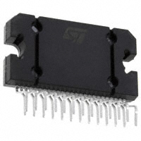
TDA7490L
20W + 20W STEREO CLASS-D AMPLIFIER
40W MONO IN BTL
1
FEATURES
Figure 1. Package
■
20W + 20W OUTPUT POWER:
@RL = 8Ω/4Ω; THD = 10%
■
HIGH EFFICIENCY
WIDE SUPPLY VOLTAGE RANGE (FROM ±10
TO ±25V)
SPLIT SUPPLY, SINGLE SUPPLY
OPERATION
TURN OFF/ON POP FREE
ST-BY AND MUTE FEATURES
SHORT CIRCUIT PROTECTION ACROSS
THE LOAD
THERMAL OVERLOAD PROTECTION
EXTERNALLY SINCHRONIZABLE
BRIDGE CONFIGURATION
■
■
■
■
■
■
■
■
Flexiwatt 25
Table 1. Order Codes
2
Part Number
Package
TDA7490L
Flexiwatt 25
c
u
d
DESCRIPTION
)
s
t(
o
r
P
The TDA7490L is a dual audio class D amplifier
assembled in Flexiwatt 25 package; it is specially
designed for high efficiency application mainly for
TV and Home Stereo sets.
e
t
le
o
s
b
O
-
Figure 2. Test and Application Circuit. (Stereo Configuration)
R1 10K
R17 52.3K
MUTE
STBY
R2
30K
R3
10K
R21 4.7K
6
INPUT1
10
o
r
P
e
C2
1nF
C26 470pF C25 470pF
(t s)
c
u
d
7
9
C23
2200µF
14
+VCC
C22
100nF
2
C21
2200µF
t
e
l
o
C4
100nF
R1 10K
bs
O
R15
100
5
INTEGRATOR1
3
12
C3
100nF
C19
560pF
L1 30µ
C18 330pF
OUT1
C10
220nF
R14 22K
8
OSC
16
EXT_CK
C17
24pF
1
C7 100nF
-VCC
C20
33nF
11
13
-VCC
-VCC
4
PWM-stage1
G=2.5
PREAMPLIFIER1
-VCC
R4
130K
R20
68K
C27
2.2µF
C1 330nF
+VCC
15
R13
10K
C16 330pF
25
R 6.8
C5 330nF
INPUT2
C6
1nF
PREAMPLIFIER2
18
PWM-stage2
G=2.5
19
R5 4.7K
23
INTEGRATOR2
17
21
20
24
22
L2 30µ
R12 22K
C15
560pF
C14
33nF
OUT2
C29
220nF
R11
100
C8 470pF
-VCC
R6
68K
C9 470pF
C28
2200µF
-VCC
C11
100nF
C12
2200µF
+VCC
D98AU978A
R9 52.3K
December 2005
Rev. 2
1/11
TDA7490L
Figure 3. Test and Application Circuit. (Bridge Configuration)
470pF
C40
C41
R4
68K
7
INPUT
R5 52.3K
470pF
The LC filter is optimized for 8Ω
(LC filter for 4Ω in single-ended)
It hos to be changed for other loads
9
-
10
L9 30µ
Int.
PWM-stage
+
PRE
3
C23
235nF
C26
470nF
dumping
(common
mode)
R27
10
R63
4.7K
C24
235nF
+
PRE
18
Int.
PWM-stage
23
C29
470nF
L10 30µ
-
19
R25
Rload
R28
10
17
470pF
c
u
d
470pF
C60 R61
68K
C59
R62 52.3K
)
s
t(
o
r
P
D99AU1081
e
t
le
Table 2. Absolute Maximum Ratings
Symbol
Parameter
VCC
DC Supply Voltage (no signal)
Ptot
Power Dissipation Tcase = 70°C
Tstg, Tj
(s)
o
s
b
O
-
ct
Storage and Junction Temperature
u
d
o
Operating Temperature Range
Top
V6,8,10,18
r
P
e
Maximum Voltage on pins # 6,8,10,18 referred to GND
t
e
l
o
Value
Unit
±30
V
35
W
–40 to 150
°C
0 to 70
°C
±5
V
Value
Unit
1
°C/W
Table 3. Thermal Data
Symbol
s
b
O
Rth j-case
2/11
Parameter
Thermal Resistance Junction-case
Typ.
TDA7490L
Figure 4. Application in Supply Voltage
52.3K
1
1
*
R3
1 2
1
2
+VSP2
-VSP2
N.C.
IN 2
FEED3
18
FEED4
2
BOOT2
2
2
2
R12
1
21
C15
560pF
C14
22
24
20
22K
1
23
2
1
1
2
2
470pF
100uF
1
e
t
le
C11
470pF
C9
2
R5
4.7K
+Vs
1
R6
68K
R9
2
2
1
C8
2
1
2
c
u
d
30uH
L2
C29
2
OUT 1
EXT_CK
)
s
t(
1
2
OUT 2
220nF
o
r
P *
R11
100
C6
1
1
1
1
15
2
10K
33nF
17
1nF
19
330nF
C5
10V REG
2
1
IN 2
25
1
R13
330pF
1
OUT2
100nF
C17 24pF
1
T2
-VS
220nF
R14
22K
2
-5V REG
1
2
2
8
C16
16
1
OSC
1
2
C10
2
2 1
TDA7490L
C4 100nF
C18
330pF
2
1
1
SGND
2
1
1
3
11
2
T1
13
1
*
L1 30uF
2
+5V REG
100nF
C7
C12
C19
560pF
1 2
2
C20
5
2200uF
R23
2
1
OUT1
12
C3
BOOT1
*
R15
33nF
1
1
4
+VSP1
9
2
-VSP1
C2
1nF
100
CURREF
330nF
1K
130K
FEED2
C1
FEED1
2
IN 1
7
6
MUTE
2
10
2
1
2
68K
14
1 uF
*
C21
2200uF
2
1
R20
2
1
1K
R4
C27
U1
IN 1
R22
2
1
+Vs
1
2
4.7K
10k
2
1
1
2
R21
1
+Vs
C22
470pF
C25
1
2
1
2
30k
Stby
1
1
Mute
+VS
R2
2
2
1
10K
R17
2
100nF
2
2
2
1
C26
470pF
1
R1
New component
o
s
b
O
1
52.3K
)
s
(
ct
u
d
o
r
P
e
t
e
l
o
s
b
O
3/11
TDA7490L
Figure 5. Pin Connection
Name
1
-VCC sign/sub
2
-VCCpow1
3
out 1
4
+VCCpow1
5
BOOT1
6
STBY-MUTE
7
FEED1
8
OSC
9
FEED2
10
IN1
11
T1
+5V
13
GND
t
e
l
o
14
15
16
s
b
O
17
Function
Negative signal/substrate supply
CURREF
T2
-5V
FEED3
PWM output of CH1
Bootstrap CH1
Control State Pin
Feedback pin 1 CH1
)
s
(
ct
Feedback pin2 CH1
u
d
o
Input CH1
Triangular waveform CH1
+5V regulator (only for internal purposes)
Signal ground
Setting current resistor
Triangular waveform CH2
-5V regulator (only for internal purposes)
Feedback pin1 CH2
19
FEED4
20
NC
Not connected
21
BOOT2
Bootstrap CH2
22
+VCCpow2
OUT2
-VCCpow2
25
Vreg
4/11
Input CH2
Feedback pin2 CH2
Positive power supply CH2
PWM output of CH2
Negative power supply CH2
10V regulator
-VCC
Vreg
c
u
d
o
r
P
Master Oscillator Setting Freequency Pin (or external sync.)
IN2
24
o
s
b
O
-
Positive power supply CH1
18
23
e
t
le
Negative power supply CH1
r
P
e
12
+VCC
D97AU816B
Table 4. Pin Description
Pin N°
OUT2
N.C.
BOOT2
IN2
FEED4
FEED3
T2
-5V
GND
CURREF
T1
+5V
IN1
OSC
FEED2
FEED1
STBY-MUTE
+VCC
BOOT1
-VCC
25
OUT1
-VCC
1
)
s
t(
TDA7490L
Table 5. Electrical Characteristics
(Refer to the test circuit, VCC = ±19V; RL = 8Ω; Demod. filter L = 30µH, C = 220nF; f = 1KHz; fsw = 200kHz;
Tamb = 25°C unless otherwise specified.)
Symbol
Parameter
Test Condition
VS
Supply Range
Iq
Total Quiescent Current
Po
Po(BTL)
RL = ∞ no LC filter
PD
mA
mV
Output Power in Bridge
Configuration
VS = ±20V; RL = 16Ω
THD = 10%
THD=1%
40
32
W
W
VS =±15.5V; RL = 8Ω
THD = 10%
THD=1%
40
32
W
W
RL = 4Ω Vcc=±13.5V
THD = 10%
THD=1%
18
14.5
VCC = ±19V; RL = 8Ω
Pο = 20W + 20W; THD = 10%
Po = 20W + 20W
RL = 8Ω; Po = 1 W
Imax
Overcurrent Protection
Threshold
RL = 0
Tj
Thermal Shut-down Junction
Temperature
Gv
Closed Loop Gain
Gain Matching
eN
Total Input Noise
RG = 50Ω
CT
Cross talk
Ri
Input Resistance
o
s
b
O
-
e
t
le
Pr
29
)
s
(
ct
u
d
o
Supply Voltage Rejection
Overvoltage Threshold
(5)
Tr, Tt
uc
od
86
f = 100Hz; Vr = 0.5
%
%
5
A
150
°C
30
31
dB
+1
dB
7
12
20
W
0.1
-1
f = 1 KHz, Po = 1W
SVR
)
s
t(
W
W
5.6
A Curve
f = 20Hz to 22KHz
Vrmax
µV
µV
55
dB
30
kΩ
60
dB
55
60
V
Rising and Falling Time
50
70
ns
Power Transistor on Resistance
0.4
0.8
Ω
200
230
KHz
0
07
V
r
P
e
t
e
l
o
(4)
120
+150
W
W
Efficiency (')
RDSON
V
20
16
Total Harmonic Distortion
(3)
Unit
±25
THD = 10%
THD= 1%
Maximum Dissipated Power
η
Max.
Output Power
THD
Fsw
70
-150
Output Power
Po(1)
Typ.
±10
Output Offset Voltage
VOS
∆Gv
Min.
Switching Frequency Range
100
MUTE & STAND-BY FUNCTIONS
s
b
O
VST-BY
Stand-by range
VMUTE
Mute Range
1.7
2.5
V
VPLAY
Play Range
4
5
V
AMUTE
Mute Attenuation
55
IqST-BY
Quiescent Current @ Stand-by
60
3
dB
5
mA
*: Po = measured across the load using the following inductor: COIL58120 MPPA 2 (magnectics) TURNS= 20∅ 1 mm
(1) L = 15µH, C = 470nF
(3) ∆Gv is intended with R2, R17, R5, R9 1% precision
(4) Fsw = 0.25 · (1/(300ns + R13 · (C17 + 76pF) . 0.85)
(5) VRMAX = (+Vcc) - (-Vcc) when VR ≥VRMAX the device goes in Stand-By mode
5/11
TDA7490L
Figure 6. P.C. Board and Component Layout of the Figs. 2, 3 (for Stereo and Bridge Compatible
Configuration)
Component
Side
c
u
d
e
t
le
)
s
(
ct
u
d
o
r
P
e
t
e
l
o
s
b
O
6/11
o
s
b
O
-
)
s
t(
o
r
P
Solder
Side
TDA7490L
Figure 10. Frequency Response
Figure 7. Distortion vs. Output Power
10
AMP
(dB)
THD (%)
5
D99AU1103
2
2
Stereo
0
Vcc=+/-19V
1
Rl = 8 ohm
-2
f = 1KHz
0.5
Filter AES
VS= ±17V;
Rl= 8Ω;
0dB= 1W
-4
0.2
-6
0.1
-8
0.05
-10
0.02
-12
0.01
200m
500m
1
2
5
10
20
-14
0.01
30
0.1
1
10
f(KHz)
Pout (W)
THD(%)
10
Stereo
Vs=± 19V
7
Vs=+/-13.5V, Rl=4Ohm
2
Rl = 8 ohm
f = 1KHz
6
f = 1KHz
e
t
le
1
5
0.5
4
0.2
o
r
P
o
s
b
O
3
0.1
2
0.05
0.02
0.01
200m
500m
1
2
5
c
u
d
Pout(W)
o
r
P
e
(t s)
10
CT
(dB)
bs
0
0.5
2
4
6
8
10
12
14
16
18
20
2xPo(W)
Figure 12. Distortion vs. Output Power in BTL
THD (%)
D99AU1102
t
e
l
o
-20
1
20
Figure 9. Crosstalk vs. Frequency
-30
c
u
d
Ptot(W)
8
5
)
s
t(
Figure 11. Power Dissipation vs. Output Power
Figure 8. Distortion vs. Output Power
10
5
VS ± 17V;
Rl=8Ω;
0dB=1W
BTL
Vcc=+/-15.5 V
2
1
-40
Rl = 8ohm
f = 1KHZ
Filter AES
O
0.5
-50
0.2
-60
0.1
-70
0.05
-80
-90
-100
0.001
0.02
0.01
0.1
1
f(KHz)
0.01
200m
500m
1
2
5
10
20
50
Pout (W)
7/11
TDA7490L
Figure 13. Distortion vs. Output Power in BTL
THD (%) 10
5
25
Pout (W)
BTL
Stereo
Vcc=+/-20V
2
Figure 14. Pout vs Supply Voltage
20
Rl = 8ohm
Rl=16ohm
THD=10%
f = 1KHZ
f = 1KHz
1
Filter AES
15
0.5
10
0.2
THD=1%
0.1
5
0.05
0.02
0
0.01
200m
500m
1
2
5
10
20
50
10
12
Pout (W)
14
16
Vs ( +/-V)
18
c
u
d
e
t
le
)
s
(
ct
u
d
o
r
P
e
t
e
l
o
s
b
O
8/11
o
s
b
O
-
o
r
P
20
)
s
t(
TDA7490L
Figure 15. Flexiwatt 25 Mechanical Data & Package Dimensions
DIM.
A
B
C
D
E
F (1)
G
G1
H (2)
H1
H2
H3
L (2)
L1
L2 (2)
L3
L4
L5
M
M1
N
O
R
R1
R2
R3
R4
V
V1
V2
V3
MIN.
4.45
1.80
0.75
0.37
0.80
23.75
28.90
22.07
18.57
15.50
7.70
3.70
3.60
mm
TYP.
4.50
1.90
1.40
0.90
0.39
1.00
24.00
29.23
17.00
12.80
0.80
22.47
18.97
15.70
7.85
5
3.5
4.00
4.00
2.20
2
1.70
0.5
0.3
1.25
0.50
MAX.
4.65
2.00
MIN.
0.175
0.070
1.05
0.42
0.57
1.20
24.25
29.30
0.029
0.014
0.031
0.935
1.139
22.87
19.37
15.90
7.95
0.869
0.731
0.610
0.303
4.30
4.40
0.145
0.142
inch
TYP.
0.177
0.074
0.055
0.035
0.015
0.040
0.945
1.150
0.669
0.503
0.031
0.884
0.747
0.618
0.309
0.197
0.138
0.157
0.157
0.086
0.079
0.067
0.02
0.12
0.049
0.019
MAX.
0.183
0.079
0.041
0.016
0.022
0.047
0.955
1.153
0.904
0.762
0.626
0.313
0.169
0.173
(1): dam-bar protusion not included
(2): molding protusion included
V
(s)
t
c
u
d
o
r
P
e
V3
e
t
le
o
s
b
O
R3
R4
V1
R2
N
L2
L4
A
H2
R
L3
O
C
V
t
e
l
o
bs
o
r
P
H
H1
H3
O
c
u
d
)
s
t(
Flexiwatt25 (vertical)
5˚ (T p.)
3˚ (Typ.)
20˚ (Typ.)
45˚ (Typ.)
B
OUTLINE AND
MECHANICAL DATA
L
L1
V1
V2
R2
D
R1
L5
Pin 1
R1
R1
E
G
G1
F
FLEX25ME
M
M1
7034862
9/11
TDA7490L
Table 6. Revision History
Date
Revision
Description of Changes
March 2001
1
First Issue
December 2005
2
Corrected the value of the inductance in the caption of the Table 5
“Electrical Characteristics”.
c
u
d
e
t
le
)
s
(
ct
u
d
o
r
P
e
t
e
l
o
s
b
O
10/11
o
s
b
O
-
o
r
P
)
s
t(
TDA7490L
c
u
d
e
t
le
)
s
(
ct
)
s
t(
o
r
P
o
s
b
O
-
u
d
o
r
P
e
t
e
l
o
Information furnished is believed to be accurate and reliable. However, STMicroelectronics assumes no responsibility for the consequences
of use of such information nor for any infringement of patents or other rights of third parties which may result from its use. No license is granted
by implication or otherwise under any patent or patent rights of STMicroelectronics. Specifications mentioned in this publication are subject
to change without notice. This publication supersedes and replaces all information previously supplied. STMicroelectronics products are not
authorized for use as critical components in life support devices or systems without express written approval of STMicroelectronics.
s
b
O
The ST logo is a registered trademark of STMicroelectronics.
All other names are the property of their respective owners
© 2005 STMicroelectronics - All rights reserved
STMicroelectronics group of companies
Australia - Belgium - Brazil - Canada - China - Czech Republic - Finland - France - Germany - Hong Kong - India - Israel - Italy - Japan Malaysia - Malta - Morocco - Singapore - Spain - Sweden - Switzerland - United Kingdom - United States of America
www.st.com
11/11
很抱歉,暂时无法提供与“TDA7490L”相匹配的价格&库存,您可以联系我们找货
免费人工找货