TDA7515
RF front-end for AM/FM-DSP car radios with IF sampling
Features
■
RF AGC generation by RF and IF detection
■
I/Q Mixer for FM IF 10.7MHz with image
rejection and programmable IF tank adjust for
FM and AM
■
Preamplifier and mixer for IF 10.7MHz AM
upconversion
■
VCO and programmable divider for “world
receiver”
■
Programmable controlled IF-gain stage
■
High performance fast PLL for RDS-system
■
Electronic alignment for the preselection
stages
■
All functions bus-controlled
u
d
o
r
P
e
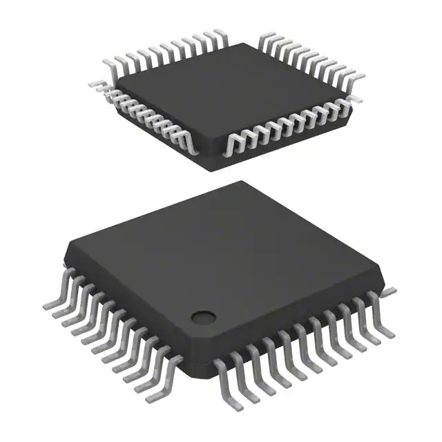
LQFP44
t
e
l
o
It contains mixer and IF amplifiers for AM and FM,
VCO and PLL synthesizer on a single chip.
)
(s
Description
)
s
(
ct
s
b
O
Use of BICMOS technology allows the
implementation of several tuning functions and a
minimum of external components.
t
c
u
The front-end is a high performance tuner circuit
for AM/FM - DSP car radios with 10.7MHz - IF
sampling.
P
e
d
o
r
Order codes
t
e
l
o
s
b
O
Part numbers
Package
Packing
TDA7515
LQFP44 (10x 10x 1.4mm)
Tray
TDA7515TR
LQFP44 (10x 10x 1.4mm)
Tape and reel
November 2006
Rev 2
1/7
www.st.com
7
�Block diagram and pin description
1
TDA7515
Block diagram and pin description
Figure 1.
Block diagram
optional
2
AGC
2
2
ADJ
IF 10.7MHz
2
FM
u
d
o
Bus
Interface
AGC
TV1
TV2
2
AM
e
t
e
ol
PM
1/4
1/8
DIV
1/6
1/10
)
(s
00AT0037
t
c
u
:1/:2/:3
VCO
PLL
LPOUT
LPAM
Pr
Supply
REFDIV
LPFM
LPHC
s
b
O
Fref
18/100kHz
t
e
l
o
SDA
Fref-
IFAMAGCTC
Fref+
Vref
DAGC
IFGND
IFOUT2
IFOUT1
P
e
IFAGCTC
d
o
r
VCCIF
Pin connection
33 32 31 30 29 28 27 26 25 24 23
bs
VCC
34
22
SCL
IFINAM
35
21
GNDPLL
17
LPOUT
MIXOUT2
40
16
LPAM/SW
AMAGCTC
41
15
VPLL
FMIFAGCin
42
14
VCOE
AMIN2
43
13
VCOB
AMIN1
44
12
GNDVCO
00AT0036
1
2
3
4
5
6
7
8
9
10 11
VCCVCO
O
TV2
39
TV1
LPREF
MIXOUT1
FMAGCTC
18
FMIN2
38
RFGND
LPFM
IFIN2
FMIN1
LPHC
19
FMPINDR
20
37
AMPINDR
36
AMRFAGCin
GND
IFIN1
AMRFAGCout
Figure 2.
2/7
)
s
(
ct
AGC
Q
I
PM
DAGC
2
�TDA7515
Block diagram and pin description
Table 1.
Pin description
Pin No.
Pin Name
1
AMRFAGCin
2
AMRFAGCout AM AGC output for RF AGC
AMPINDR
4
FMPINDR
5
FMIN1
FM mixer input 1
6
RFGND
RF ground
7
FMIN2
8
FMAGCTC
O
AM AGC pin-diode driver
FM AGC pin-diode driver
FM mixer input 2
FM AGC time constant
9
TV1
Tuning voltage 1 output
10
TV2
Tuning voltage 2 output
11
VCCVCO
Supply voltage VCO
12
GNDVCO
VCO ground
13
VCOB
Base VCO
14
VCOE
Emitter VCO
15
VPLL
PLL supply voltage
)
s
(
ct
u
d
o
r
P
e
16
LPAM/SW
17
LPOUT
OPAMP output to PLL loop filter
18
LPREF
Voltage reference for PLL
19
LPFM
OP AMP input to PLL loop filter FM
20
LPHC
High current PLL loop filter
21
GNDPLL
22
SCL
Bus connection (IIC clock)
23
SDA
Bus connection (IIC data)
24
IFAMAGCTC
25
Fref-
27
o
s
b
AM AGC input for RF detection
3
P
e
28
OP AMP input to PLL loop filter AM / switch output (optional)
t
e
l
o
)
(s
PLL ground
s
b
O
t
c
u
d
o
r
26
let
Function
Time constant for AM IF AGC
Reference frequency input
Fref+
Reference frequency input
Vref
Reference voltage 5V
DAGC
Digital keying AGC input
29
IFGND
IF ground
30
IFOUT2
IF amplifier output
31
IFOUT1
IF amplifier output
32
VCCIF
Supply voltage for IF output
33
IFAGCTC
34
VCC
35
IFINAM
IF AGC time constant
Supply voltage
IF input for narrowband AM
36
GND
Ground
37
IFIN1
IF Input - signal
38
IFIN2
IF Input - blocked
39
MIXOUT1
Mixer output
40
MIXOUT2
Mixer output
41
AMAGCTC
AM AGC time constant
42
FMIFAGCin
43
AMIN2
AM RF input
44
AMIN1
AM RF input
IF input for FM AGC
3/7
�Electrical specifications
TDA7515
2
Electrical specifications
2.1
Thermal data
Table 2.
Thermal data
Values
Symbol
Parameter
Unit
Min.
Rth(j-a)
2.2
Thermal resistance
85
°C/W
Ambient temperature
-40
85
°C
Tstg
Storage temperature
-55
150
°C
Table 3.
Supply voltage for IF-interface
VPLL
PLL supply voltage
VCCVCO
VCO supply voltage
VCC
t(s
c
u
d
o
r
P
o
s
b
O
)
Supply voltage
VMIXOUT1/2 Open collector voltage
e
t
e
ol
e
t
e
l
Parameter
VCCIF
)
s
(
t
c
u
d
Absolute maximum ratings
Symbol
4/7
Max.
Tamb
Absolute maximum ratings
s
b
O
Typ.
o
r
P
Value
Unit
12
V
12
V
12
V
12
V
12
V
�TDA7515
3
Package information
Package information
In order to meet environmental requirements, ST offers these devices in ECOPACK®
packages. These packages have a lead-free second level interconnect. The category of
second level interconnect is marked on the package and on the inner box label, in
compliance with JEDEC standard JESD97. The maximum ratings related to soldering
conditions are also marked on the inner box label.
ECOPACK is an ST trademark. ECOPACK specifications are available at: www.st.com.
Figure 3.
LQFP44 (10x10) Mechanical data & package dimensions
mm
MIN.
TYP.
A
MAX.
MIN.
TYP.
1.60
A1
0.05
A2
1.35
0.15
0.002
1.40
1.45
0.053
0.055
0.37
0.45
0.012
0.015
0.20
0.004
B
0.30
0.09
D
11.80
12.00
12.20
0.464
D1
9.80
10.00
10.20
0.386
8.00
0.480
0.394
0.401
0.315
12.20
0.464
0.472
E1
9.80
10.00
10.20
0.386
0.394
8.00
L
d
o
r
k
ccc
)
(s
0.315
0.60
1.00
t
e
l
o
s
b
O
0.480
0.401
0.031
t
c
u
0.45
L1
r
P
e
0.018
0.472
12.00
0.80
0.057
0.008
11.80
e
u
d
o
0.006
E
E3
OUTLINE AND
MECHANICAL DATA
MAX.
0.063
C
D3
)
s
(
ct
inch
DIM.
0.75
0.018
0.024
0.030
0.039
LQFP44 (10 x 10 x 1.4mm)
0˚(min.), 3.5˚(typ.), 7˚(max.)
0.10
0.0039
P
e
t
e
l
o
s
b
O
0076922 E
5/7
�Revision history
4
TDA7515
Revision history
Table 4.
Document revision history
Date
Revision
Changes
24-Jan-2006
1
Initial release.
24-Nov-2006
2
Package changed, layout changes, text modification.
)
s
(
ct
u
d
o
r
P
e
t
e
l
o
)
(s
t
c
u
d
o
r
P
e
t
e
l
o
s
b
O
6/7
s
b
O
�TDA7515
)
s
(
ct
Please Read Carefully:
u
d
o
Information in this document is provided solely in connection with ST products. STMicroelectronics NV and its subsidiaries (“ST”) reserve the
right to make changes, corrections, modifications or improvements, to this document, and the products and services described herein at any
time, without notice.
r
P
e
All ST products are sold pursuant to ST’s terms and conditions of sale.
Purchasers are solely responsible for the choice, selection and use of the ST products and services described herein, and ST assumes no
liability whatsoever relating to the choice, selection or use of the ST products and services described herein.
t
e
l
o
No license, express or implied, by estoppel or otherwise, to any intellectual property rights is granted under this document. If any part of this
document refers to any third party products or services it shall not be deemed a license grant by ST for the use of such third party products
or services, or any intellectual property contained therein or considered as a warranty covering the use in any manner whatsoever of such
third party products or services or any intellectual property contained therein.
)
(s
s
b
O
UNLESS OTHERWISE SET FORTH IN ST’S TERMS AND CONDITIONS OF SALE ST DISCLAIMS ANY EXPRESS OR IMPLIED
WARRANTY WITH RESPECT TO THE USE AND/OR SALE OF ST PRODUCTS INCLUDING WITHOUT LIMITATION IMPLIED
WARRANTIES OF MERCHANTABILITY, FITNESS FOR A PARTICULAR PURPOSE (AND THEIR EQUIVALENTS UNDER THE LAWS
OF ANY JURISDICTION), OR INFRINGEMENT OF ANY PATENT, COPYRIGHT OR OTHER INTELLECTUAL PROPERTY RIGHT.
t
c
u
UNLESS EXPRESSLY APPROVED IN WRITING BY AN AUTHORIZED ST REPRESENTATIVE, ST PRODUCTS ARE NOT
RECOMMENDED, AUTHORIZED OR WARRANTED FOR USE IN MILITARY, AIR CRAFT, SPACE, LIFE SAVING, OR LIFE SUSTAINING
APPLICATIONS, NOR IN PRODUCTS OR SYSTEMS WHERE FAILURE OR MALFUNCTION MAY RESULT IN PERSONAL INJURY,
DEATH, OR SEVERE PROPERTY OR ENVIRONMENTAL DAMAGE. ST PRODUCTS WHICH ARE NOT SPECIFIED AS "AUTOMOTIVE
GRADE" MAY ONLY BE USED IN AUTOMOTIVE APPLICATIONS AT USER’S OWN RISK.
d
o
r
P
e
t
e
l
o
Resale of ST products with provisions different from the statements and/or technical features set forth in this document shall immediately void
any warranty granted by ST for the ST product or service described herein and shall not create or extend in any manner whatsoever, any
liability of ST.
s
b
O
ST and the ST logo are trademarks or registered trademarks of ST in various countries.
Information in this document supersedes and replaces all information previously supplied.
The ST logo is a registered trademark of STMicroelectronics. All other names are the property of their respective owners.
© 2006 STMicroelectronics - All rights reserved
STMicroelectronics group of companies
Australia - Belgium - Brazil - Canada - China - Czech Republic - Finland - France - Germany - Hong Kong - India - Israel - Italy - Japan Malaysia - Malta - Morocco - Singapore - Spain - Sweden - Switzerland - United Kingdom - United States of America
www.st.com
7/7
�
很抱歉,暂时无法提供与“TDA7515”相匹配的价格&库存,您可以联系我们找货
免费人工找货