TDA7535
Delta/sigma cascade 20 bit stereo DAC
Features
■
20-bit resolution single ended output
■
Analog reconstruction third order Chebyshev
filter
■
I2S input data format
■
On chip PLL
■
System clock: 64 Fs
■
2 output channels
■
0.9 VRMS single ended output dynamic
■
3.3 V power supply
■
Reset
■
Sampling rate 36 kHz to 48 kHz
)
s
(
ct
u
d
o
r
P
e
Description
t
e
l
o
)
(s
The TDA7535 is a stereo, digital-to-analog
converter designed for audio application,
including digital interpolation filter, a third order
multi-bit Delta-Sigma DAC, a third order
Chebyshev's reconstruction filter and a differential
to single ended output converter. This device is
fabricated in highly advanced CMOS, where high
speed precision analog circuits are combined with
high density logic circuits. The TDA7535,
according to standard audio converters, can
accept any I2S data format.
t
c
u
d
o
r
P
e
t
e
l
o
s
b
O
Table 1.
SO14
s
b
O
The TDA7535 is available in SO14 package. The
total power consumption is less than 75 mW.
TDA7535 is suitable for a wide variety of
applications where high performance are
required. Its low cost and single 3.3 V power
supply make it ideal for several applications, such
as CD players, MPEG audio, MIDI applications,
CD-ROM drives, CD-Interactive, digital radio
applications and so on. An evaluation board is
available to perform measurement and to make
listening tests.
Device summary
Order code
Package
Packing
TDA7535
SO14
Tube
TDA7535013TR
SO14
Tape and reel
February 2009
Rev 8
1/12
www.st.com
12
�Contents
TDA7535
Contents
1
Block diagram and pin description . . . . . . . . . . . . . . . . . . . . . . . . . . . . . 3
2
Electrical specification . . . . . . . . . . . . . . . . . . . . . . . . . . . . . . . . . . . . . . . 4
2.1
Absolute maximum ratings . . . . . . . . . . . . . . . . . . . . . . . . . . . . . . . . . . . . . 4
2.2
Thermal data . . . . . . . . . . . . . . . . . . . . . . . . . . . . . . . . . . . . . . . . . . . . . . . 4
2.3
Recommended DC operating conditions . . . . . . . . . . . . . . . . . . . . . . . . . . 4
2.4
Power consumption . . . . . . . . . . . . . . . . . . . . . . . . . . . . . . . . . . . . . . . . . . 5
2.5
General interface electrical characteristics . . . . . . . . . . . . . . . . . . . . . . . . . 5
2.6
Low voltage CMOS interface DC electrical characteristics . . . . . . . . . . . . 5
2.7
DAC electrical characteristics . . . . . . . . . . . . . . . . . . . . . . . . . . . . . . . . . . . 6
)
s
(
ct
u
d
o
r
P
e
3
I2S interface . . . . . . . . . . . . . . . . . . . . . . . . . . . . . . . . . . . . . . . . . . . . . . . . 7
4
Application circuit . . . . . . . . . . . . . . . . . . . . . . . . . . . . . . . . . . . . . . . . . . . 9
5
Package information . . . . . . . . . . . . . . . . . . . . . . . . . . . . . . . . . . . . . . . . 10
6
Revision history . . . . . . . . . . . . . . . . . . . . . . . . . . . . . . . . . . . . . . . . . . . 11
t
e
l
o
)
(s
t
c
u
d
o
r
P
e
t
e
l
o
s
b
O
2/12
s
b
O
�TDA7535
1
Block diagram and pin description
Block diagram and pin description
Figure 1.
I2S
I2S
Block diagram
DIGITAL
INPUT 20
FIR1
FIR2
FIR3
20
FS
PLL
8FS
ALU
CLKOUT
23
S&H
ΣΔ MODULATOR
64FS
4
THERMO DECODER &
RANDOMIZER
DIFF TO SINGLE
CONVERTER
D02AU1417
Figure 2.
Pin connection (top view)
N.C.
1
14
SDATA
2
13
SCK
3
N.C.
4
GND_DIG
5
GND_ANA
6
OUTSR
Table 2.
od
7
FSYNC
VDD_DIG
11
N.C.
10
VDD_ANA
9
VCM
8
OUTSL
D01AU1276A
Input/output power
N.C.
-
-
SDATA
I
I2S digital data input
3
SCK
I
I2S clock input
4
N.C.
-
-
5
GND_DIG
P
Digital ground
6
GND_ANA
P
Analog ground
7
OUTSR
O
Right channel single ended output
8
OUTSL
O
Left channel single ended output
9
VCM
P
Reference 1.65 V externally filtered
10
VDD_ANA
P
Analog 3.3 V supply
11
N.C.
-
-
12
VDD_DIG
P
Digital 3.3 V-supply
13
FSYNC
I
I2S Left-right channel selector
14
RESETN
I
Reset (active low)
2
b
O
-O
RESETN
Pin name
1
e
t
e
l
so
t
c
u
Pin function
Pin #
(s)
bs
u
d
o
r
P
e
t
e
l
o
12
ANALOG
OUTPUT
)
s
(
ct
3rd CHEBYSHEV
SC FILTER
Pr
Description
3/12
�Electrical specification
TDA7535
2
Electrical specification
2.1
Absolute maximum ratings
Table 3.
Absolute maximum ratings
Symbol
Parameter
-0.5 to +4.6
-0.5 to +4.6
V
V
Power supplies
Vaio
Analog input and output voltage
-0.5 to (VCC+0.5)
V
Vdio
Digital input and output voltage
-0.5 to (VDD+0.5)
Vdi5
Digital input voltage (5 V tolerant)
-0.5 to 6.5
Operating junction temperature range
-40 to 125
(s)
Tstg
°C
°C
t
e
l
o
)
(s
t
c
u
od
Pr
Rth j-amb
V
Operation at or beyond these limit may result in permanent
damage to the device. Normal operation is not guaranteed at
these extremes.
Thermal data
Symbol
-55 to 150
V
r
P
e
Thermal data
Table 4.
ct
u
d
o
Storage temperature
Warning:
2.2
Unit
VDD
VCC
Tj
Digital
Analog
Value
s
b
O
Parameter
Thermal resistance junction to ambient (1)
Value
Unit
85
°C/W
e
t
e
ol Recommended DC operating conditions
1. In still air.
2.3
s
b
O
Table 5.
Recommended DC operating conditions
Symbol
Parameter
VDD
VCC
4/12
Test condition
Min.
Typ.
Max.
Unit
3.3 V digital power supply voltage
3.15
3.3
3.45
V
3.3 V analog power supply voltage
3.15
3.3
3.45
V
�TDA7535
Electrical specification
2.4
Power consumption
Table 6.
Power consumption
Symbol
Idd
Parameter
Test condition
Total maximum current
Min.
Power supply @ 3.3 V and Tj = 125 °C
2.5
General interface electrical characteristics
Table 7.
General interface electrical characteristics
Symbol
Parameter
Test condition
lil
Low level input current
without pull-up device
Vi = 0 V(1)
lih
High level input current
without pull-up device
Vi = Vdd (1)
I/O latch-up current
V < 0 V, V > Vdd
Ilatchup
Electrostatic protection
Vesd
Leakage, 1
Min.
Max.
Unit
21.5
25
mA
Typ.
Max.
Unit
1
μA
1
μA
)
s
(
ct
u
d
o
r
P
e
200
μA(2)
Typ.
t
e
l
o
mA
2000
V
1. The leakage currents are generally very small,
很抱歉,暂时无法提供与“TDA7535”相匹配的价格&库存,您可以联系我们找货
免费人工找货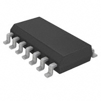


 工商网监
湘ICP备2023018690号
工商网监
湘ICP备2023018690号