TDA7803A
High efficiency digital input automotive quad power amplifier with
built-in diagnostics features, ’start stop’ compatible
Datasheet - production data
Programmable diagnostic pin
CMOS compatible enable pin
Thermal protection
'!0'03�����
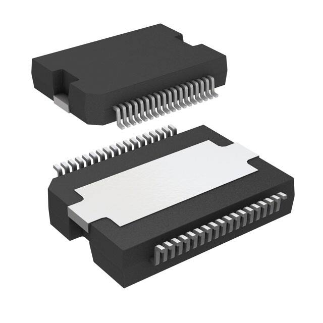
PowerSO-36
'!0'03�����
Pop free in mute to play transitions and viceversa
Flexiwatt 27 (SMD)
Description
The TDA7803A is a single chip quad bridge
amplifier in advanced BCD technology
integrating: a full D/A converter, digital input for
direct connection to I2S (or TDM) and powerful
MOSFET output stages.
'!0'03�����
'!0'03�����
Flexiwatt 27
(horizontal)
Flexiwatt 27
(vertical)
Features
The integrated D/A converter allows the
performance to reach an outstanding 115 dB S/N
ratio with more than 110 dB of dynamic range.
AEC-Q100 qualified
24-bit digital processing
115 dB dynamic range (A-weighted)
SB-I (SB - improved) high efficiency operation
the highest ’non - class D’ efficiency
Parallel mode function availability
High output power capability:
– 4 x 27 W 4Ω@ 14.4 V, 1 kHz, THD = 10%
– 4 x 47 W 2 Ω @ 14.4 V, 1 kHz, THD = 10%
Flexible mode control:
– Full I2C bus driving 1.8V/3.3V) with four
addresses selectable (only for PowerSO36
package option)
– Independent front/rear play/ mute
– Selectable digital gains for very-low noise
line-out function
– Digital diagnostic with DC and AC load
detections
Start-stop compatibility (operation down to 6V)
Sample rates: 44.1 kHz, 48 kHz, 96 kHz, 192 kHz
Flexible serial data port (1.8 V / 3.3 V):
– I2S standard, TDM 4Ch, TDM 8Ch, TDM
16ch (8+8ch)
Moreover the TDA7803A integrates an innovative
high efficiency concept, optimized also for
uncorrelated music signals. The device is
designed to be compatible to battery modulation
for class-G systems.
Thanks to this concept, the dissipated “output
power” under average listening conditions can be
reduced up to 50% when compared to the
conventional class AB solutions.
The TDA7803A integrates also a programmable
PLL that is able to lock at the input frequencies of
64*Fs for all the input configurations.
The device is equipped with a full diagnostics array
that communicates the status of each speaker
through the I2C bus. The same I2C bus allows to
control several configurations of the device.
The TDA7803A is able to play music down to 6 V
supply voltage - so it is compatible with the so
called 'start stop' battery profile recently adopted
by several car makers (thus reducing the fuel
consumption and the impact over the
environment).
Offset detector
Independent front/rear clipping detector
January 2019
This is information on a product in full production.
DS12195 Rev 5
1/72
www.st.com
�Contents
TDA7803A
Contents
1
Block diagram and pins description . . . . . . . . . . . . . . . . . . . . . . . . . . . . 8
1.1
Block diagram . . . . . . . . . . . . . . . . . . . . . . . . . . . . . . . . . . . . . . . . . . . . . . . 8
1.2
Pins description . . . . . . . . . . . . . . . . . . . . . . . . . . . . . . . . . . . . . . . . . . . . . 8
2
Application diagrams . . . . . . . . . . . . . . . . . . . . . . . . . . . . . . . . . . . . . . . 11
3
Electrical specification . . . . . . . . . . . . . . . . . . . . . . . . . . . . . . . . . . . . . . 12
4
3.1
Absolute maximum ratings . . . . . . . . . . . . . . . . . . . . . . . . . . . . . . . . . . . . 12
3.2
Thermal data . . . . . . . . . . . . . . . . . . . . . . . . . . . . . . . . . . . . . . . . . . . . . . 12
3.3
Electrical characteristics . . . . . . . . . . . . . . . . . . . . . . . . . . . . . . . . . . . . . . 13
3.4
Electrical characteristics typical curves . . . . . . . . . . . . . . . . . . . . . . . . . . 17
Operation states . . . . . . . . . . . . . . . . . . . . . . . . . . . . . . . . . . . . . . . . . . . 22
4.1
Standby state . . . . . . . . . . . . . . . . . . . . . . . . . . . . . . . . . . . . . . . . . . . . . . 22
4.2
ECO-mode state . . . . . . . . . . . . . . . . . . . . . . . . . . . . . . . . . . . . . . . . . . . . 22
4.3
Amplifier-mode state . . . . . . . . . . . . . . . . . . . . . . . . . . . . . . . . . . . . . . . . . 22
4.4
Turn-on and permanent diagnostic . . . . . . . . . . . . . . . . . . . . . . . . . . . . . . 22
5
Operation compatibility vs. battery . . . . . . . . . . . . . . . . . . . . . . . . . . . . 24
6
Functional description . . . . . . . . . . . . . . . . . . . . . . . . . . . . . . . . . . . . . . 25
2/72
6.1
Voltage regulators timing . . . . . . . . . . . . . . . . . . . . . . . . . . . . . . . . . . . . . 25
6.2
Turn-on diagnostic description . . . . . . . . . . . . . . . . . . . . . . . . . . . . . . . . . 25
6.3
Permanent diagnostic . . . . . . . . . . . . . . . . . . . . . . . . . . . . . . . . . . . . . . . . 29
6.4
AC diagnostic . . . . . . . . . . . . . . . . . . . . . . . . . . . . . . . . . . . . . . . . . . . . . . 31
6.5
Input offset detector . . . . . . . . . . . . . . . . . . . . . . . . . . . . . . . . . . . . . . . . . 31
6.6
Double faults . . . . . . . . . . . . . . . . . . . . . . . . . . . . . . . . . . . . . . . . . . . . . . 32
6.7
Thermal protection . . . . . . . . . . . . . . . . . . . . . . . . . . . . . . . . . . . . . . . . . . 32
6.8
Voltage monitoring feature and ADC characteristics . . . . . . . . . . . . . . . . 33
6.9
Mute management . . . . . . . . . . . . . . . . . . . . . . . . . . . . . . . . . . . . . . . . . . 34
6.9.1
Auto-mute threshold . . . . . . . . . . . . . . . . . . . . . . . . . . . . . . . . . . . . . . . . 35
6.9.2
Mute and unmute commutation time . . . . . . . . . . . . . . . . . . . . . . . . . . . 35
DS12195 Rev 5
�TDA7803A
7
8
9
10
Contents
6.10
Class SBI - Improved high efficiency principle . . . . . . . . . . . . . . . . . . . . . 35
6.11
High power and parallel mode configuration . . . . . . . . . . . . . . . . . . . . . . 36
6.12
Power on reset threshold . . . . . . . . . . . . . . . . . . . . . . . . . . . . . . . . . . . . . 36
Additional features . . . . . . . . . . . . . . . . . . . . . . . . . . . . . . . . . . . . . . . . . 37
7.1
Noise gating . . . . . . . . . . . . . . . . . . . . . . . . . . . . . . . . . . . . . . . . . . . . . . . 37
7.2
Tri-state mode . . . . . . . . . . . . . . . . . . . . . . . . . . . . . . . . . . . . . . . . . . . . . 37
I2S and TDM bus interface . . . . . . . . . . . . . . . . . . . . . . . . . . . . . . . . . . . 38
8.1
I2S and TDM input data frame format . . . . . . . . . . . . . . . . . . . . . . . . . . . 38
8.2
I2S input data format . . . . . . . . . . . . . . . . . . . . . . . . . . . . . . . . . . . . . . . . 39
8.3
TDM input data format . . . . . . . . . . . . . . . . . . . . . . . . . . . . . . . . . . . . . . . 39
8.4
Timings requirements . . . . . . . . . . . . . . . . . . . . . . . . . . . . . . . . . . . . . . . . 41
8.5
Group delay . . . . . . . . . . . . . . . . . . . . . . . . . . . . . . . . . . . . . . . . . . . . . . . 42
I2C bus interface . . . . . . . . . . . . . . . . . . . . . . . . . . . . . . . . . . . . . . . . . . . 43
9.1
Writing procedure . . . . . . . . . . . . . . . . . . . . . . . . . . . . . . . . . . . . . . . . . . . 44
9.2
Reading procedure . . . . . . . . . . . . . . . . . . . . . . . . . . . . . . . . . . . . . . . . . . 44
9.3
Data validity . . . . . . . . . . . . . . . . . . . . . . . . . . . . . . . . . . . . . . . . . . . . . . . 44
9.4
Start and stop conditions . . . . . . . . . . . . . . . . . . . . . . . . . . . . . . . . . . . . . 44
9.5
Byte format . . . . . . . . . . . . . . . . . . . . . . . . . . . . . . . . . . . . . . . . . . . . . . . . 44
9.6
Acknowledge . . . . . . . . . . . . . . . . . . . . . . . . . . . . . . . . . . . . . . . . . . . . . . 44
9.7
Address selection . . . . . . . . . . . . . . . . . . . . . . . . . . . . . . . . . . . . . . . . . . . 45
9.8
I2C bus timings . . . . . . . . . . . . . . . . . . . . . . . . . . . . . . . . . . . . . . . . . . . . . 45
I2C registers . . . . . . . . . . . . . . . . . . . . . . . . . . . . . . . . . . . . . . . . . . . . . . . 46
10.1
Instruction byte . . . . . . . . . . . . . . . . . . . . . . . . . . . . . . . . . . . . . . . . . . . . . 46
10.1.1
IB0 - Subaddress "I0000000h" - default = "00000000" . . . . . . . . . . . . . 46
10.1.2
IB1 - Subaddress "I0000001h" - default = "00000000" . . . . . . . . . . . . . 47
10.1.3
IB2 - Subaddress "I0000010h" - default = "00000000" . . . . . . . . . . . . . 48
10.1.4
IB3 - Subaddress "I0000011h" - default = "00000000" . . . . . . . . . . . . . 49
10.1.5
IB4 - Subaddress "I0000100h" - default = "00000000" . . . . . . . . . . . . . 50
10.1.6
IB5 - Subaddress "I0000101h" - default = "00000000" . . . . . . . . . . . . . 51
10.1.7
IB6 - Subaddress "I0000110h" - default = "00000000" . . . . . . . . . . . . . 52
10.1.8
IB7 - Subaddress "I0000111h" - default = "00000000" . . . . . . . . . . . . . 53
DS12195 Rev 5
3/72
4
�Contents
TDA7803A
10.2
11
Data byte . . . . . . . . . . . . . . . . . . . . . . . . . . . . . . . . . . . . . . . . . . . . . . . . . 54
10.2.1
DB0 - Subaddress: "I0010000h" . . . . . . . . . . . . . . . . . . . . . . . . . . . . . . 54
10.2.2
DB1 - Subaddress: "I0010001h" - Channel 1 . . . . . . . . . . . . . . . . . . . . 55
10.2.3
DB2 - Subaddress: "I0010010h" - Channel 2 . . . . . . . . . . . . . . . . . . . . 56
10.2.4
DB3 - Subaddress: "I0010011h" - Channel 3 . . . . . . . . . . . . . . . . . . . . . 57
10.2.5
DB4 - Subaddress: "I0010100h" - Channel 4 . . . . . . . . . . . . . . . . . . . . 58
10.2.6
DB5 - Subaddress: "I0010101h" . . . . . . . . . . . . . . . . . . . . . . . . . . . . . . 59
10.2.7
DB6 - Subaddress: "I0010110h" . . . . . . . . . . . . . . . . . . . . . . . . . . . . . . 60
10.2.8
DB7 - Subaddress: "I0010111h" - Vcc level ADC conversion . . . . . . . . 60
Package information . . . . . . . . . . . . . . . . . . . . . . . . . . . . . . . . . . . . . . . . 61
11.1
PowerSO-36 (slug up) package information . . . . . . . . . . . . . . . . . . . . . . 61
11.2
Flexiwatt 27 (vertical) package information . . . . . . . . . . . . . . . . . . . . . . . 63
11.3
Flexiwatt 27 (SMD) package information . . . . . . . . . . . . . . . . . . . . . . . . . 65
11.4
Flexiwatt 27 (horizontal) package information . . . . . . . . . . . . . . . . . . . . . 67
11.5
Package marking information . . . . . . . . . . . . . . . . . . . . . . . . . . . . . . . . . . 69
12
Order codes . . . . . . . . . . . . . . . . . . . . . . . . . . . . . . . . . . . . . . . . . . . . . . . 70
13
Revision history . . . . . . . . . . . . . . . . . . . . . . . . . . . . . . . . . . . . . . . . . . . 71
4/72
DS12195 Rev 5
�TDA7803A
List of tables
List of tables
Table 1.
Table 2.
Table 3.
Table 4.
Table 5.
Table 6.
Table 7.
Table 8.
Table 9.
Table 10.
Table 11.
Table 12.
Table 13.
Table 14.
Table 15.
Table 16.
Table 17.
Table 18.
Table 19.
Table 20.
Table 21.
Table 22.
Table 23.
Table 24.
Table 25.
Table 26.
Table 27.
Table 28.
Table 29.
Table 30.
Table 31.
Table 32.
Table 33.
Table 34.
Table 35.
Table 36.
Flexiwatt27 pins description . . . . . . . . . . . . . . . . . . . . . . . . . . . . . . . . . . . . . . . . . . . . . . . . . 9
PowerSO36 pins description. . . . . . . . . . . . . . . . . . . . . . . . . . . . . . . . . . . . . . . . . . . . . . . . 10
Absolute maximum ratings . . . . . . . . . . . . . . . . . . . . . . . . . . . . . . . . . . . . . . . . . . . . . . . . . 12
Thermal data. . . . . . . . . . . . . . . . . . . . . . . . . . . . . . . . . . . . . . . . . . . . . . . . . . . . . . . . . . . . 12
Electrical characteristics . . . . . . . . . . . . . . . . . . . . . . . . . . . . . . . . . . . . . . . . . . . . . . . . . . . 13
Start-up pulse typical timings (Fs = 48 kHz) . . . . . . . . . . . . . . . . . . . . . . . . . . . . . . . . . . . . 28
Double faults priority . . . . . . . . . . . . . . . . . . . . . . . . . . . . . . . . . . . . . . . . . . . . . . . . . . . . . . 32
VCC value express by 8 bit with thermometric code . . . . . . . . . . . . . . . . . . . . . . . . . . . . . . 33
Transition play to mute strategy . . . . . . . . . . . . . . . . . . . . . . . . . . . . . . . . . . . . . . . . . . . . . 34
Mute and unmute commutation time. . . . . . . . . . . . . . . . . . . . . . . . . . . . . . . . . . . . . . . . . . 35
System input frequencies . . . . . . . . . . . . . . . . . . . . . . . . . . . . . . . . . . . . . . . . . . . . . . . . . . 38
I2S interface timing . . . . . . . . . . . . . . . . . . . . . . . . . . . . . . . . . . . . . . . . . . . . . . . . . . . . . . . 41
Address threshold . . . . . . . . . . . . . . . . . . . . . . . . . . . . . . . . . . . . . . . . . . . . . . . . . . . . . . . . 45
I2C bus interface timing. . . . . . . . . . . . . . . . . . . . . . . . . . . . . . . . . . . . . . . . . . . . . . . . . . . . 45
IB0 - Subaddress "I0000000h" - default = "00000000" . . . . . . . . . . . . . . . . . . . . . . . . . . . . 46
IB1 - Subaddress "I0000001h" - default = "00000000" . . . . . . . . . . . . . . . . . . . . . . . . . . . . 47
IB2 - Subaddress "I0000010h" - default = "00000000" . . . . . . . . . . . . . . . . . . . . . . . . . . . . 48
IB3 - Subaddress "I0000011h" - default = "00000000" . . . . . . . . . . . . . . . . . . . . . . . . . . . . 49
IB4 - Subaddress "I0000100h" - default = "00000000" . . . . . . . . . . . . . . . . . . . . . . . . . . . . 50
IB5 - Subaddress "I0000101h" - default = "00000000" . . . . . . . . . . . . . . . . . . . . . . . . . . . . 51
IB6 - Subaddress "I0000110h" - default = "00000000" . . . . . . . . . . . . . . . . . . . . . . . . . . . . 52
IB7 - Subaddress "I0000111h" - default = "00000000" . . . . . . . . . . . . . . . . . . . . . . . . . . . 53
DB0 - Subaddress: "I0010000h" . . . . . . . . . . . . . . . . . . . . . . . . . . . . . . . . . . . . . . . . . . . . . 54
DB1 - Subaddress: "I0010001h" - Channel 1 . . . . . . . . . . . . . . . . . . . . . . . . . . . . . . . . . . . 55
DB2 - Subaddress: "I0010010h" - Channel 2 . . . . . . . . . . . . . . . . . . . . . . . . . . . . . . . . . . . 56
DB3 - Subaddress: "I0010011h" - Channel 3 . . . . . . . . . . . . . . . . . . . . . . . . . . . . . . . . . . . 57
DB4 - Subaddress: "I0010100h" - Channel 4 . . . . . . . . . . . . . . . . . . . . . . . . . . . . . . . . . . . 58
DB5 - Subaddress: "I0010101h" . . . . . . . . . . . . . . . . . . . . . . . . . . . . . . . . . . . . . . . . . . . . . 59
DB6 - Subaddress: "I0010110h" . . . . . . . . . . . . . . . . . . . . . . . . . . . . . . . . . . . . . . . . . . . . . 60
DB7 - Subaddress: "I0010111h" - Vcc level ADC conversion . . . . . . . . . . . . . . . . . . . . . . 60
PowerSO-36 (slug up) package mechanical data. . . . . . . . . . . . . . . . . . . . . . . . . . . . . . . . 61
Flexiwatt 27 (vertical) package mechanical data . . . . . . . . . . . . . . . . . . . . . . . . . . . . . . . . 63
Flexiwatt 27 (SMD) package mechanical data . . . . . . . . . . . . . . . . . . . . . . . . . . . . . . . . . . 65
Flexiwatt 27 (horizontal) package mechanical data . . . . . . . . . . . . . . . . . . . . . . . . . . . . . . 67
Ordering information . . . . . . . . . . . . . . . . . . . . . . . . . . . . . . . . . . . . . . . . . . . . . . . . . . . . . . 70
Document revision history. . . . . . . . . . . . . . . . . . . . . . . . . . . . . . . . . . . . . . . . . . . . . . . . . . 71
DS12195 Rev 5
5/72
5
�List of figures
TDA7803A
List of figures
Figure 1.
Figure 2.
Figure 3.
Figure 4.
Figure 5.
Figure 6.
Figure 7.
Figure 8.
Figure 9.
Figure 10.
Figure 11.
Figure 12.
Figure 13.
Figure 14.
Figure 15.
Figure 16.
Figure 17.
Figure 18.
Figure 19.
Figure 20.
Figure 21.
Figure 22.
Figure 23.
Figure 24.
Figure 25.
Figure 26.
Figure 27.
Figure 28.
Figure 29.
Figure 30.
Figure 31.
Figure 32.
Figure 33.
Figure 34.
Figure 35.
Figure 36.
Figure 37.
Figure 38.
Figure 39.
Figure 40.
Figure 41.
Figure 42.
Figure 43.
Figure 44.
Figure 45.
Figure 46.
Figure 47.
Figure 48.
6/72
Block diagram (Flexiwatt27) . . . . . . . . . . . . . . . . . . . . . . . . . . . . . . . . . . . . . . . . . . . . . . . . . 8
Pins connection diagrams. . . . . . . . . . . . . . . . . . . . . . . . . . . . . . . . . . . . . . . . . . . . . . . . . . . 8
I2C bus mode application diagram (Flexiwatt)) . . . . . . . . . . . . . . . . . . . . . . . . . . . . . . . . . . 11
I2C bus mode application diagram (PowerSO) . . . . . . . . . . . . . . . . . . . . . . . . . . . . . . . . . . 11
Quiescent current vs. supply voltage . . . . . . . . . . . . . . . . . . . . . . . . . . . . . . . . . . . . . . . . . 17
Output power vs. supply voltage (4 Ω) . . . . . . . . . . . . . . . . . . . . . . . . . . . . . . . . . . . . . . . . 17
Output power vs. supply voltage (2 Ω, STD mode) . . . . . . . . . . . . . . . . . . . . . . . . . . . . . . 18
Distortion vs. output power (4 Ω, STD mode) . . . . . . . . . . . . . . . . . . . . . . . . . . . . . . . . . . . 18
Distortion vs. output power (4 Ω, SBI mode) . . . . . . . . . . . . . . . . . . . . . . . . . . . . . . . . . . . 18
Distortion vs. output power (2 Ω, STD mode) . . . . . . . . . . . . . . . . . . . . . . . . . . . . . . . . . . . 18
Distortion vs. output power (2 Ω, SBI mode) . . . . . . . . . . . . . . . . . . . . . . . . . . . . . . . . . . . 18
Distortion vs. frequency (4 Ω) . . . . . . . . . . . . . . . . . . . . . . . . . . . . . . . . . . . . . . . . . . . . . . . 18
Distortion vs. frequency (2 Ω) . . . . . . . . . . . . . . . . . . . . . . . . . . . . . . . . . . . . . . . . . . . . . . . 19
Distortion vs. output power (4 Ω, Vs = 6 V). . . . . . . . . . . . . . . . . . . . . . . . . . . . . . . . . . . . . 19
Distortion vs. output power (2 Ω, Vs = 6 V). . . . . . . . . . . . . . . . . . . . . . . . . . . . . . . . . . . . . 19
Vo vs. Vin (Gv1-2-3-4 settings). . . . . . . . . . . . . . . . . . . . . . . . . . . . . . . . . . . . . . . . . . . . . . 19
Vo vs. Vin (Gv1-2-3-4 settings + 6 dB dig. gain). . . . . . . . . . . . . . . . . . . . . . . . . . . . . . . . . 19
Distortion vs. output voltage (LD-Gv2) . . . . . . . . . . . . . . . . . . . . . . . . . . . . . . . . . . . . . . . . 19
Distortion vs. output voltage (LD-Gv3) . . . . . . . . . . . . . . . . . . . . . . . . . . . . . . . . . . . . . . . . 20
Distortion vs. output voltage (LD-Gv4) . . . . . . . . . . . . . . . . . . . . . . . . . . . . . . . . . . . . . . . . 20
Output attenuation vs. Vs . . . . . . . . . . . . . . . . . . . . . . . . . . . . . . . . . . . . . . . . . . . . . . . . . 20
Crosstalk vs. frequency (STD mode) . . . . . . . . . . . . . . . . . . . . . . . . . . . . . . . . . . . . . . . . . 20
Crosstalk vs. frequency (SBI mode) . . . . . . . . . . . . . . . . . . . . . . . . . . . . . . . . . . . . . . . . . . 20
Supply voltage rejection vs. frequency . . . . . . . . . . . . . . . . . . . . . . . . . . . . . . . . . . . . . . . . 20
Total power dissipation & efficiency vs. Po (4 Ω, STD, Sine) . . . . . . . . . . . . . . . . . . . . . . . 21
Total power dissipation & efficiency vs. Po (4 Ω, SBI, Sine). . . . . . . . . . . . . . . . . . . . . . . . 21
Total power dissipation & efficiency vs. Po (2 Ω, SBI, Sine). . . . . . . . . . . . . . . . . . . . . . . . 21
Power dissipation vs. average Po (audio program simulation, 4 Ω) . . . . . . . . . . . . . . . . . . 21
Power dissipation vs. average Po (audio program simulation, 2 Ω) . . . . . . . . . . . . . . . . . . 21
ITU R-ARM frequency response, weighting filter for transient pop. . . . . . . . . . . . . . . . . . . 21
State diagram . . . . . . . . . . . . . . . . . . . . . . . . . . . . . . . . . . . . . . . . . . . . . . . . . . . . . . . . . . . 23
Operation compatibility vs. battery . . . . . . . . . . . . . . . . . . . . . . . . . . . . . . . . . . . . . . . . . . . 24
Soft short diagnostic . . . . . . . . . . . . . . . . . . . . . . . . . . . . . . . . . . . . . . . . . . . . . . . . . . . . . . 26
Short circuit and open load diagnostic . . . . . . . . . . . . . . . . . . . . . . . . . . . . . . . . . . . . . . . . 27
Short to GND and short to Vs, threshold description . . . . . . . . . . . . . . . . . . . . . . . . . . . . . 27
Short across the speaker and open load threshold description, in speaker mode . . . . . . . 27
Short across the speaker and open load threshold description, line driver mode . . . . . . . 28
Permanent diagnostic flow-chart. . . . . . . . . . . . . . . . . . . . . . . . . . . . . . . . . . . . . . . . . . . . . 30
Thermal muting diagram . . . . . . . . . . . . . . . . . . . . . . . . . . . . . . . . . . . . . . . . . . . . . . . . . . . 33
Low voltage mute attenuation, supply voltage variation (Vs); result digital attenuation (At) . 35
I2S format . . . . . . . . . . . . . . . . . . . . . . . . . . . . . . . . . . . . . . . . . . . . . . . . . . . . . . . . . . . . . . 39
TDM 16 (8+8) - channel format. . . . . . . . . . . . . . . . . . . . . . . . . . . . . . . . . . . . . . . . . . . . . . 39
TDM 8-channel format . . . . . . . . . . . . . . . . . . . . . . . . . . . . . . . . . . . . . . . . . . . . . . . . . . . . 40
TDM 16 (8+8) - channel format. . . . . . . . . . . . . . . . . . . . . . . . . . . . . . . . . . . . . . . . . . . . . . 40
Audio interface timing . . . . . . . . . . . . . . . . . . . . . . . . . . . . . . . . . . . . . . . . . . . . . . . . . . . . . 41
I2C bus protocol description . . . . . . . . . . . . . . . . . . . . . . . . . . . . . . . . . . . . . . . . . . . . . . . . 43
I2C bus interface timing. . . . . . . . . . . . . . . . . . . . . . . . . . . . . . . . . . . . . . . . . . . . . . . . . . . . 45
PowerSO-36 (slug up) package outline . . . . . . . . . . . . . . . . . . . . . . . . . . . . . . . . . . . . . . . 61
DS12195 Rev 5
�TDA7803A
Figure 49.
Figure 50.
Figure 51.
Figure 52.
Figure 53.
List of figures
Flexiwatt 27 (vertical) package outline . . . . . . . . . . . . . . . . . . . . . . . . . . . . . . . . . . . . . . . . 63
Flexiwatt 27 (SMD) package outline . . . . . . . . . . . . . . . . . . . . . . . . . . . . . . . . . . . . . . . . . . 65
Flexiwatt 27 (horizontal) package outline . . . . . . . . . . . . . . . . . . . . . . . . . . . . . . . . . . . . . . 67
PowerSO-36 marking information. . . . . . . . . . . . . . . . . . . . . . . . . . . . . . . . . . . . . . . . . . . . 69
Flexiwatt 27 marking information . . . . . . . . . . . . . . . . . . . . . . . . . . . . . . . . . . . . . . . . . . . . 69
DS12195 Rev 5
7/72
7
�Block diagram and pins description
TDA7803A
1
Block diagram and pins description
1.1
Block diagram
Figure 1. Block diagram (Flexiwatt27)
,�&
&'�',$*
6'$ 6&/
��
3//
:6
�
�
6&.
��
6'��
��
6'��
��
67%<
�
,�6��
LQWHUIDFH
��
,�&
'LDJQ�
,QWHUSRO�
��)V
�
1RLVH
VKDSHU
67�%<
$�'
9&&�� 9&&��
��
��
�
��
7KHUPRPHWULF
&RGH
&RQYHUVLRQ
�
'':$
���[��
&XUUHQW�
JHQHUDWRUV
DUUD\
7KHUPRPHWULF
&RGH
&RQYHUVLLRQ
�
'':$
���[��
&XUUHQW�
JHQHUDWRUV
DUUD\
7KHUPRPHWULF
&RGH
&RQYHUVLRQ
�
'':$
���[��
&XUUHQW�
JHQHUDWRUV
DUUD\
)XOO\�%DODQFHG
7UDQVUHVLVWDQFH
3RZHU�)LOWHU
7KHUPRPHWULF
&RGH
&RQYHUVLRQ
�
'':$
���[��
&XUUHQW�
JHQHUDWRUV
DUUD\
)XOO\�%DODQFHG
7UDQVUHVLVWDQFH
3RZHU�)LOWHU
�� 287��
)XOO\�%DODQFHG
7UDQVUHVLVWDQFH
3RZHU�)LOWHU
)XOO\�%DODQFHG
7UDQVUHVLVWDQFH
3RZHU�)LOWHU
�
�
287��
�
�
287��
�
�
287��
�� 287��
�� 287��
�� 287��
��
�
287��
9&&
��
��
'�9� '*1'
��
��
�
��
��
�
��
$�9�
$*1'
7$%
3:*1'�
3:*1'�
�
�
�
3:*1'� 3:*1'�
*$3*36�����
1.2
Pins description
Figure 2. Pins connection diagrams
Flexiwatt27
��
3#,
��
3$!
��
#$�$)!'
��
/54��
��
07'.$�
��
/54�
��
4!"
��
�
4!"
/54�
��
�
/54�
6##��
��
�
6##��
6##��
07'.$�
��
�
07'.$�
��
/54�
/54��
��
�
/54��
��
07'.$�
��
/54��
.#
��
�
.#
��
!�6�
!�6�
��
�
#$�$)!'
��
$�6�
$�6�
��
�
3$!
��
!'.$
!'.$
��
�
��
$'.$
3#,
��
3$��
$'.$
��
��
!$$
��
3$��
3$��
��
��
34"9
��
3#+
3$��
��
��
73
��
/54��
3#+
��
��
5.-54%HW
�
07'.$�
�
/54�
/54��
��
��
/54��
�
6##��
07'.$�
��
��
07'.$�
�
/54�
�
07'.$�
6##��
��
��
6##��
�
/54��
/54�
��
��
/54�
�
73
4!"
��
��
�
34"9
�
4!"
4!"
*$3*36�����
*$3*36�����
8/72
PowerSO
DS12195 Rev 5
�TDA7803A
Block diagram and pins description
Table 1. Flexiwatt27 pins description
N°
Pin
1
TAB
2
STBY
3
WS
4
OUT2+
5
PWGND2
6
Function
TAB connection
Ground
STBY pin
Input
2
Word select (I S bus)
Logic Input
Channel 2 (Left Rear) positive output
Power Output
Power ground channels 2
Power Ground
OUT2-
Channels 2 (Left Rear) negative output
Power Output
7
VCC12
Channel 1 and 2 positive supply
8
OUT1-
Channel 1 (Left Front) negative output
Power Output
9
PWGND1
Power ground channel 1
Power Ground
10
OUT1+
Channel 1 (Left Front) positive output
Power Output
2S
Battery
bus)
Logic Input
11
SCK
Serial clock (I
12
SD24
Serial data channels 2 and 4 (I2S bus)
2S
bus)
Logic Input
Logic Input
13
SD13
Serial data channels 1 and 3 (I
14
DGND
Digital ground
Signal Ground
15
AGND
Analog ground
Signal Ground
16
D3V3
Digital 3.3V supply filter
Digital Regulator
17
A3V3
Analog 3.3V supply filter
Analog Regulator
18
OUT3+
19
PWGND3
20
Channels 3 (right front) positive output
Power Output
Power ground channel 3
Power Ground
OUT3-
Channels 3 (right front) negative output
Power Output
21
VCC34
Channels 3 and 4 positive supply
22
OUT4-
Channels 4 (right rear) negative output
Power Output
23
PWGND4
Power ground channel 4
Power Ground
24
OUT4+
Channels 4 (right rear) positive output
Power Output
25
CD/DIAG
26
27
SDA
SCL
Clip detector and diagnostic output
Battery
Open Drain Output
2
Signal Input
2
Signal Input
I C data
I C clock
DS12195 Rev 5
9/72
71
�Block diagram and pins description
TDA7803A
Table 2. PowerSO36 pins description
N°
Pin
1
TAB
2
OUT4-
Channels 4 (right rear) negative output
3
VCC34
Channels 3 and 4 positive supply
4
PWGND4
5
OUT4+
Device slug connection
Ground
Power Output
Battery
Power ground channel 4
Power Ground
Channels 4 (right rear) positive output
Power Output
6
NC
7
CD/DIAG
8
SDA
I2C data
Signal Input
SCL
I2
Signal Input
10
ADD
I2C Address
Logic Input
11
STBY
STBY pin
9
Not connected
-
Clip detector and diagnostic output
C clock
Word select
WS
13
UNMUTEhw
14
OUT2+
15
PWGND2
16
VCC12
Channel 1 and 2 positive supply
17
OUT2-
Channels 2 (Left Rear) negative output
18
TAB
bus)
Logic Input
Unmute Hardware
Logic Input
Channel 2 (Left Rear) positive output
Power Output
Power ground channels 2
Power Ground
Battery
Device slug connection
TAB
20
OUT1-
Channel 1 (Left Front) negative output
21
VCC12
Channel 1 and 2 positive supply
22
PWGND1
23
OUT1+
25
SD24
Power Output
Ground
19
SCK
Open Drain Output
Input
(I2S
12
24
10/72
Function
Device slug connection
Ground
Power Output
Battery
Power ground channel 1
Power Ground
Channel 1 (Left Front) positive output
Power Output
Serial clock
(I2S
bus)
Logic Input
Serial data channels 2 and 4
(I2S
bus)
(I2S
bus)
Logic Input
26
SD13
Serial data channels 1 and 3
27
DGND
Digital ground
Signal Ground
28
AGND
Analog ground
Signal Ground
29
D3V3
Digital 3.3V supply filter
Digital Regulator
30
A3V3
Analog 3.3V supply filter
Analog Regulator
31
NC
Not connected
32
OUT3+
33
PWGND3
34
VCC34
Channels 3 and 4 positive supply
35
OUT3-
Channels 3 (right front) negative output
36
TAB
Logic Input
-
Channels 3 (right front) positive output
Power Output
Power ground channel 3
Power Ground
Device slug connection
DS12195 Rev 5
Battery
Power Output
Ground
�TDA7803A
2
Application diagrams
Application diagrams
Figure 3. I2C bus mode application diagram (Flexiwatt))
9V
&�
����)
&�
�����)
9&&��
9&&��
�
67%<
��
�
��
�
287�5)���287�
��
��
�
�
��
��
,�&�%86
6'$
��
6&/
��
287�55����287�
��
7'$����$
�
�
��
287�/)���287�
�
,�6�,1387
:6
�
�
6&.
��
6'��
��
�
6'��
��
�
�
�
287�/5���287�
�
��
��
��
�
��
��
$�9�
'�9�
&���
�
��)
'*1' $*1'
�
7$%
5��
&���
�
���)
9
��N
&'�',$*
�
��&HUDPLF��;�5��W\SHV�UHFRPPHQGHG�
*$'*����������36
Figure 4. I2C bus mode application diagram (PowerSO)
9V
&�
����)
&�
�����)
9&&�� 9&&�� 9&&�� 9&&��
��
67%<
��
��
�
��
��
�
,�6�,1387
6'$
�
6&/
�
:6
��
6&.
��
6'��
��
6'��
��
$''
�VHH�1RWH���
��
5��
��N
&�
�
��
7'$����$
��
�
�
287�/)���287�
�
�
287�/5���287�
��
��
��
�������������
��
��
��
$�9�
�)
&���
�
��)
�
7$%
�
'�9�
&���
�
���)
�
��&HUDPLF��;�5��W\SHV�UHFRPPHQGHG�
1. Refer to Section 9:
287�55����287�
��
��
'*1' $*1'
I2C
�
�
�
��
81087(KZ
287�5)���287�
��
��
,�&�%86
�
5��
9
��N
&'�',$*
*$'*����������36
bus interface for connection suggestions.
DS12195 Rev 5
11/72
71
�Electrical specification
TDA7803A
3
Electrical specification
3.1
Absolute maximum ratings
Table 3. Absolute maximum ratings
Symbol
VS
Parameter
Value
Unit
DC supply voltage
-0.3 to 28
V
Transient supply voltage for t = 100 ms
-0.3 to 50
V
2
-0.3 to 4.6
V
2
I S bus pins voltage
-0.3 to 4.6
V
Unmute hardware voltage (PSO36 only)
-0.3 to 4.6
V
CD/Diag pin voltage
-0.3 to 20
V
STBY pin voltage
-0.3 to 4.6
V
Output peak current (repetitive f > 10 Hz)
internally
limited(1)
A
85
W
Storage and junction temperature
55 to 150
°C
Tamb
Operative temperature range(2)
-40 to 105
°C
Cmax
Maximum capacitor vs. ground connected to the output
Vpeak
Vi2c
Vi2s
Vunmute
Vcd
Vstby
IO
Ptot
Tstg, Tj
ESDHBM
ESDCDM
I C bus pins voltage
Power dissipation Tcase = 70 °C
4.7
nF
ESD protection HBM
(3)
2000
V
ESD protection CDM
(3)
500
V
1. Internally limited by overcurrent protection.
2. A suitable heatsink/dissipation system should be used to keep Tj inside the specified limits.
3. Conforming to Q100 ESD standard.
3.2
Thermal data
Table 4. Thermal data
Symbol
Rth j-case
12/72
Parameter
Thermal resistance junction-to-case (max.)
DS12195 Rev 5
Value
Unit
1
°C/W
�TDA7803A
3.3
Electrical specification
Electrical characteristics
Referred to the test setup VS = 14.4 V; RL = 4 Ω; f = 1 kHz; tested at Tamb = 25 °C;
functionality guaranteed for Tj = -40 °C to 150 °C; SB-I mode; unless otherwise specified.
Table 5. Electrical characteristics
Symbol
Parameter
Test condition
Min.
Typ.
Max.
Unit
RL = 4 Ω
6
-
18.5
V
RL = 2 Ω, std_bridge
6
-
16
V
RL = 2 Ω, SBI
6
-
16
V
Standby current
-
-
1
4
μA
Iq
Total quiescent current in
amplifier mode
Mute condition
-
170
210
mA
IqECO
Total quiescent current in
ECO mode
ECO mode
-
35
40
mA
AM
Mute attenuation
-
80
-
-
dB
VOS
Offset voltage
Mute and play
-25
-
+25
mV
Attenuation


 工商网监
湘ICP备2023018690号
工商网监
湘ICP备2023018690号
