®
TLPxxM/G/G-1
TRIPOLAR OVERVOLTAGE PROTECTION for TELECOM LINE
Application Specific Discretes A.S.D.™
MAIN APPLICATIONS Any sensitive telecom equipment requiring protection against lightning : Analog and ISDN line cards Main Distribution Frames Terminal and transmission equipment Gas-tube replacement PowerSO-10TM TLPxxM
TIP TIP TIP TIP TIP
GND RING RING RING RING RING
DESCRIPTION The TLPxxM/G/G-1 series are tripolar transient surge arrestors used for primary and secondary protectionin sensitive telecom equipment.
GND
FEATURES TRIPOLAR CROWBAR PROTECTION
TIP
TAB
GND
RING
VOLTAGE RANGE SELECTED TELECOM APPLICATIONS REPETITIVE PEAK PULSE CURRENT : IPP = 100 A (10 / 1000 µs) HOLDING CURRENT : IH = 150 mA LOW CAPACITANCE : C = 110 pF typ.
FOR
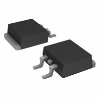
D2PAK TLPxxG
LOW LEAKAGE CURRENT : IR = 5 µA max
GND
TAB
BENEFITS No ageing and no noise. If destroyed, the TLPxxM/G/G-1 falls into short circuit, still ensuring protection. Access to Surface Mount applications thanks to the PowerSO-10TM and D2PAK package.
TIP GND RING
I2PAK TLPxxG-1
TM: ASD and PowerSO-10 are trademarks of ST Microelectronics.
September 1998 - Ed : 3C
1/14
�TLPxxM/G/G-1
COMPLIES WITH THE FOLLOWING STANDARDS: CCITT K20 VDE0433 VDE0878 IEC-1000-4-5 FCC Part 68, lightning surge type A FCC Part 68, lightning surge type B BELLCORE TR-NWT-001089 FIRST LEVEL BELLCORE TR-NWT-001089 SECOND LEVEL CNET I31-24 Peak Surge Voltage (V) 4000 4000 4000 level 4 level 4 1500 800 1000 2500 1000 5000 4000 Voltage Waveform (µs) 10/700 10/700 1.2/50 10/700 1.2/50 10/160 10/560 5/320 2/10 10/1000 2/10 0.5/700 Current Waveform (µs) 5/310 5/310 1/20 5/310 8/20 10/160 10/560 5/320 2/10 10/1000 2/10 0.8/310 Admissible Ipp (A) 100 100 100 100 100 200 100 25 500 100 500 100 Necessary Resistor (Ω) -
TYPICAL APPLICATION Primary protection module
TLPxxM/G/G-1
Analog Line Card
Main Distribution Frame
Analog line card protection
- Vbat
PTC LINE A
TLPxxM/G/G-1
LCP1511D
RING RELAY 220nF LINE B PTC
SLIC
2/14
�TLPxxM/G/G-1
TYPICAL APPLICATION ISDN: U interface protection
TLPxxM/G/G-1
1/2 DA108S1 R3
+5V
R4 R5
Internal circuitry
Power Feeder
PARAMETER MEASUREMENT INFORMATION Symbol IPP ITSM IR IRM IH VBR VR VRM VBO C Description Peak pulse current Maximum peak on-state current Leakage current Leakage current Holding current Breakdown voltage Continuous reverse voltage Maximum stand-off voltage Breakover voltage Capacitance
IH IR IRM VRM VR VBO IPP
ABSOLUTE MAXIMUM RATINGS (Tamb = 25°C) Symbol IPP Parameter Peak pulse current (longitudinal & transversal mode) : 10/1000 µs (open circuit voltage waveform 1 kV 10/1000 µs) 8/20 µs (open circuit voltage waveform 4 kV 1.2/50 µs) 2/10 µs (open circuit voltage waveform 2.5kV 2/10 µs) Mains power induction t = 200ms VRMS = 300V, R = 600Ω Mains power contact VRMS = 220V, R = 10Ω (Fail-Safe threshold) VRMS = 220V, R = 600Ω Tstg Tj TL TOP Storage temperature range Maximum operating junction temperature Maximum lead temperature for soldering during 10 s Operating temperature range t = 200 ms t = 15 mn Value 100 250 500 0.7 Unit A A A A
ITSM
31 0.42 - 55 to + 150 150 260 - 40 to + 85
A A °C °C °C °C
3/14
�TLPxxM/G/G-1
THERMAL RESISTANCE Symbol Rth (j-c) Junction to case Parameter TLPxxM TLPxxG TLPxxG-1 TLPxxM TLPxxG TLPxxG-1 Value 1.0 1.0 1.0 see table page 14 see table page 14 see table page 14 Unit °C/W °C/W
Rth (j-a)
Junction to ambient
ELECTRICAL CHARACTERISTICS BETWEEN TIP AND RING (Tamb = 25°C) IRM @ VRM max. µA 5 5 5 V 120 180 230 IR @ VR max. µA 50 50 50 V 140 200 270 C typ. note pF 35 35 35
Type
TLP140M/G/G-1 TLP200M/G/G-1 TLP270M/G/G-1
Note : VR = 50 V bias, VRMS = 1V, F = 1 MHz.
ELECTRICAL CHARACTERISTICS BETWEEN TIP AND GND, RING AND GND (Tamb = 25°C) IRM @ VRM Type max. IR @ V R max. note 1 µA TLP140M/G/G-1 TLP200M/G/G-1 TLP270M/G/G-1 5 5 5 V 120 180 230 µA 50 50 50 V 140 200 270 VBO @ IBO max. note 2 V 200 290 400 mA 500 500 500 max. IH min. note 3 mA 150 150 150 C @ VR typ. note 4 pF 110 110 110 note 5 pF 40 40 40
Note 1: IR measured at VR guarantees V BR min > VR. Note 2: Measured at 50 Hz. Note 3: See functional holding current test circuit. Note 4: VR = 0V bias, VRMS = 1V, F = 1 MHz. Note 5: VR = 50V bias, VRMS = 1V, F = 1 MHz (TIP or RING (-) / GND (+)).
4/14
�TLPxxM/G/G-1
FUNCTIONAL HOLDING CURRENT (IH) TEST CIRCUIT: GO-NO GO TEST
R - VP VBAT = - 48 V D.U.T. Surge generator
This is a GO-NO GO test which allows to confirm the holding current (IH) level in a functional test circuit. TEST PROCEDURE : - Adjust the current level at the IH value by short circuiting the D.U.T. - Fire the D.U.T. with a surge current : IPP = 10A, 10/1000µs. - The D.U.T. will come back to the off-state within a duration of 50ms max.
MARKING Package PowerSO-10 D2PAK I2PAK Types TLP140M TLP200M TLP270M TLP140G TLP200G TLP270G TLP140G-1 TLP200G-1 TLP270G-1 Marking TLP140M TLP200M TLP270M TLP140G TLP200G TLP270G TLP140G TLP200G TLP270G
ORDER CODE
TPL
Tripolar Line Protection Breakdown Voltage
270 M
- TR Packaging: -TR=tapeandreelonlyfor”M”version(600pcs) = tube (50 pcs) Package: M : Power SO10 G : D2PAK G-1 : I2PAK
5/14
�TLPxxM/G/G-1
Fig. 1: Maximum peak on-state current versus pulse duration.
ITSM(A) 100 90 80 70 60 50 40 30
TIP or RING vs GND F=50Hz Tj initial=25°C
Fig. 2: Relative variation of IH versus Tamb.
IH (Tamb) / IH (25°C) 2 1.8 1.6 1.4 1.2 1 0.8
20 10 0 0.01 t(s) 0.1 1 10 100 1000
0.6 0.4 -40 -20 0
Tamb (°C) 20 40 60 80
Fig. 3-1 :junction capacitance versus applied reverse voltage (typical values) (TLP140M/G/G-1).
200 100 50
LINE / LINE LINE- / GND+
Fig. 3-2 :junction capacitance versus applied reverse voltage (typical values) (TLP200M/G/G-1).
200 100 50
LINE / LINE LINE- / GND+
C(pF)
F=1MHz Vosc=1VRMS Tj=25° C LINE+ / GND-
C(pF)
F=1MHz Vosc=1VRMS Tj=25° C LINE+ / GND-
20 VR(V) 10 1 10 100 200
20
VR(V)
10
1
10
100
200
Fig. 3-3 :junction capacitance versus applied reverse voltage (typical values) (TLP270M/G/G-1).
C(pF) 200 100
LINE+ / GNDF=1MHz Vosc=1VRMS Tj=25° C
Fig. 4: Test diagram for breakover voltage measurement.
TIP 10 / 1000 µs 100 A surge generator VBO TIP - GND GND
VBO TIP RING
50
LINE / LINE LINE- / GND+
RING
20 VR(V) 10 1 10 100 300
6/14
�TLPxxM/G/G-1
Fig. 5-1 : Breakover voltage measurement (TLP140M/G/G-1). Fig. 5-2 : Breakover voltage measurement (TLP200M/G/G-1).
2.6 2.4 2.2 2 1.8 1.6 1.4 1.2
Vbr/Vbr
2.6 2.4
Vbo/Vbr
TIP RING
2.2 2 1.8 1.6 1.4
TIP RING
TIP+ GND TIP- GND +
0.1 1 10 dV/dt 100 1,000 10,000 100,000
1.2 1 0.01 0.1 1 10
TIP+ GND TIP- GND +
100 dV/dt 1,000 10,000 100,000
1 0.01
Fig. 5-3 : Breakover voltage measurement (TLP270M/G/G-1).
2.6 2.4 2.2 2 1.8 1.6 1.4 1.2
Vbo/Vbr
TIP RING
TIP+ GND TIP- GND +
0.1 1 10 dV/dt 100 1,000 10,000 100,000
1 0.01
7/14
�TLPxxM/G/G-1
PACKAGE MECHANICAL DATA D2PAK Plastic DIMENSIONS
A E L2 C2
REF. A A1 A2
D
Millimeters 4.30 2.49 0.03 0.70 1.40 0.45 1.21 8.95 10.00 4.88 15.00 1.27 1.40 0.40 0° 8° 0° 0.60 0.017 1.36 0.047 9.35 0.352 10.28 0.393 5.28 0.192 15.85 0.590 1.40 0.050 1.75 0.055 4.60 0.169 2.69 0.098 0.23 0.001 0.93 0.027
Inches 0.181 0.106 0.009 0.037 0.055 0.024 0.054 0.368 0.405 0.208 0.624 0.055 0.069 0.016 8°
Min. Typ. Max. Min. Typ. Max.
L L3 A1 B2 B G A2 2.0 MIN. FLAT ZONE V2 C R
B B2 C C2 D E G L L2 L3 R V2
FOOT-PRINT D2PAK
16.90
10.30 1.30
5.08
3.70 8.90
8/14
�TLPxxM/G/G-1
PACKAGE MECHANICAL DATA I2PAK Plastic DIMENSIONS Millimeters Inches Min. Typ. Max. Min. Typ. Max. A A1 B B1 B2 C C2 D e E L L1 L2 V V4 4.30 2.49 0.70 1.20 1.25 0.45 1.21 8.95 2.44 10.00 13.10 3.48 1.27 5° 45° 1.40 4.60 0.169 2.69 0.098 0.93 0.028 1.38 0.047 0.181 0.106 0.037 0.054
REF.
0.049 0.055 0.60 0.018 0.024 1.36 0.048 9.35 0.352 2.64 0.096 10.28 0.394 13.60 0.516 3.78 0.137 1.40 0.050 5° 45° 0.054 0.368 0.104 0.405 0.535 0.149 0.055
9/14
�TLPxxM/G/G-1
PACKAGE MECHANICAL DATA Power-SO10
B
0.10 A B
10 H E
6 E2 E3 E1
1
5
SEATING PLANE
e
0.25 M
B
DETAIL ”A”
A C
h
D D1
Q
A F A1
SEATING PLANE
A1 L
DETAIL ”A”
E4
a
REF. A A1 B C D D1 E E1 E2
10/14
DIMENSIONS Millimeters Inches Min. Typ. Max. 3.35 0.00 0.40 0.35 9.40 7.40 9.30 7.20 7.20 Min. Typ. Max. 0.143 0.0039 0.0236 0.0217 0.378 0.299 0.374 0.291 0.299 3.65 0.131 0.10 0.00 0.60 0.0157 0.55 0.0137 9.60 0.370 7.60 0.291 9.50 0.366 7.40 0.283 7.60 0.283
DIMENSIONS REF. E3 E4 e F H h L Q a 0° Millimeters Min. Typ. Max. 6.10 5.90 1.27 1.25 13.80 0.50 1.20 1.70 8° 0° 1.80 0.0472 0.067 8° 1.35 0.0492 14.40 0.543 0.019 0.0708 Inches Min. Typ. Max. 0.250 0.240 0.05 0.0531 0.567
6.35 0.240 6.10 0.232
�TLPxxM/G/G-1
FOOT PRINT Power-SO10 MOUNTING PAD LAYOUT RECOMMENDED HEADER SHAPE
Dimensions in millimeters SHIPPING TUBE
Dimensions in millimeters
DIMENSIONS (mm)
C B
A B C Length tube
TYP 18 12 0,8 532 50
A
Surface mount film taping : contact sales office
Quantity per tube
11/14
�TLPxxM/G/G-1
SOLDERING RECOMMENDATION The soldering process causes considerable thermal stress to a semiconductor component. This has to be minimized to assure a reliable and extended lifetime of the device. The PowerSO-10 package can be exposed to a maximum temperature of 260 °C for 10 seconds. However a proper soldering of the package could be done at 215 °C for 3 seconds. Any solder temperature profile should be within these limits. As reflow techniques are most common in surface mounting, typical heating profiles are given in Figure 1,either for mounting on FR4 or on metal-backed boards. For each particular board, the appropriate heat profile has to be adjusted experimentally. The present proposal is just a starting point. In any case, the following precautions have to be considered : - always preheat the device - peak temperatureshould be at least 30 °C higher than the melting point of the solder alloy chosen - thermal capacity of the base substrate Voids pose a difficult reliability problem for large surface mount devices. Such voids under the package result in poor thermal contact and the high thermal resistance leads to component failures. The PowerSO-10 is designed from scratch to be solely a surfacemount package, hence symmetry in the x- and y-axis gives the package excellent weight balance. Moreover, the PowerSO-10 offers the unique possibility to control easily the flatness and quality of the soldering process. Both the top and the bottom soldered edges of the package are accessible for visual inspection (soldering meniscus). Coplanarity between the substrate and the package can be easily verified. The quality of the solder joints is very important for two reasons : (I) poor quality solder joints result directly in poor reliability and (II) solder thickness affects the thermal resistance significantly. Thus a tight control of this parameter results in thermally efficient and reliable solder joints.
Fig. 1 : Typical reflow soldering heat profile Temperature (o C)
250
245 oC 215oC
200
Epoxy FR4 board
Soldering
150
Preheating
Cooling
100
Metal-backed board
50
0 0 40 80 120 160 200 240 280 320 360
Time (s)
12/14
�TLPxxM/G/G-1
SUBSTRATES AND MOUNTING INFORMATION The use of epoxy FR4 boards is quite common for surface mounting techniques, however, their poor thermal conduction compromises the otherwise outstanding thermal performanceof the PowerSO10. Some methods to overcome this limitation are discussed below. One possibility to improve the thermal conduction is the use of large heat spreader areas at the copper layer of the PC board. This leads to a reduction of thermal resistance to 35 °C for 6 cm2 of the board heatsink (see fig. 2). Use of copper-filled through holes on conventional FR4 techniques will increase the metallization and decrease thermal resistance accordingly. Using a configurationwith 16 holes under the spreader of the package with a pitch of 1.8 mm and a diameter of 0.7 mm, the thermal resistance (junction heatsink) can be reduced to 12°C/W (see fig. 3). Beside the thermal advantage, this solution allows multi-layer boards to be used. However, a drawback of this traditional material prevents its use in very high power, high current circuits. For instance, it is not advisable to surface mount devices with currents greater than 10 A on FR4 boards. A Power Mosfet or Schottky diode in a surface mount power package can handle up to around 50 A if better substrates are used.
Fig. 2 : Mounting on epoxy FR4 head dissipation by extending the area of the copper layer
Copper foil
FR4 board
Fig. 3 : Mounting on epoxy FR4 by using copper-filled through holes for heat transfer
Copper foil
FR4 board
heatsink
heat transfer
13/14
�TLPxxM/G/G-1
A new technologyavailable today is IMS - an Insulated Metallic Substrate. This offers greatly enhanced thermal characteristics for surface mount components. IMS is a substrate consisting of three different layers, (I) the base material which is available as an aluminium or a copper plate, (II) a thermal conductive dielectrical layer and (III) a copper foil, which can be etched as a circuit layer. Using this material a thermal resistance of 8°C/W 2 with 40 cm of board floating in air is achievable (see fig. 4). If even higher power is to be dissipated an external heatsink could be applied which leads to an Rth(j-a) of 3.5 °C/W (see Fig. 5), assuming that Rth (heatsink-air) is equal to Rth (junctionheatsink). This is commonly applied in practice, leading to reasonable heatsink dimensions. Often power devices are defined by considering the Fig. 4 : Mounting on metal backed board maximum junction temperature of the device. In practice , however, this is far from being exploited. A summary of various power management capabilities is made in table 1 based on a reasonable delta T of 70°C junction to air. The PowerSO-10 concept also represents an attractive alternative to C.O.B. techniques. PowerSO-10 offers devices fully tested at low and high temperature. Mounting is simple - only conventional SMT is required - enabling the users to get rid of bond wire problems and the problem to control the high temperature soft soldering as well. An optimized thermal management is guaranteed through PowerSO-10 as the power chips must in any case be mounted on heat spreaders before being mounted onto the substrate. Fig. 5 : Mounting on metal backed board with an external heatsink applied
Copper foil
Copper foil Insulation
FR4 board
Aluminium
Aluminium heatsink
TABLE 1 Printed circuit board material 1.FR4 using the recommended pad-layout 2.FR4 with heatsink on board (6cm2) 3.FR4 with copper-filled through holes and external heatsink applied 4. IMS floating in air (40 cm2) 5. IMS with external heatsink applied Rth (j-a) 50 °C/W 35 °C/W 12 °C/W 8 °C/W 3.5 °C/W P Diss 1.5 W 2.0 W 5.8 W 8.8 W 20 W
Information furnished is believed to be accurate and reliable. However, STMicroelectronics assumes no responsibility for the consequences of use of such information nor for any infringement of patents or other rights of third parties which may result from its use. No license is granted by implication or otherwise under any patent or patent rights of STMicroelectronics. Specifications mentioned in this publication are subject to change without notice. This publication supersedes and replaces all information previously supplied. STMicroelectronics products are not authorized for use as critical components in life support devices or systems without express written approval of STMicroelectronics.
The ST logo is a registered trademark of STMicroelectronics © 1998 STMicroelectronics - Printed in Italy - All rights reserved. STMicroelectronics GROUP OF COMPANIES Australia - Brazil - Canada - China - France - Germany - Italy - Japan - Korea - Malaysia - Malta - Mexico - Morocco The Netherlands - Singapore - Spain - Sweden - Switzerland - Taiwan - Thailand - United Kingdom - U.S.A. http://www.st.com 14/14
�