TM8050H-8D3
Datasheet
80 A 800 V high temperature thyristor (SCR) in D3PAK package
Features
A
G
K
A
K
G
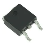
D3PAK
•
High junction temperature: Tj = 150 °C
•
Blocking voltage: VDRM = VRRM = 800 V
•
Nominal current: IT(RMS) = 80 A
•
Gate triggering current: IGT max. = 50 mA
•
High noise immunity: dV/dt > 1 kV/µs
•
•
Surface mounted device D3PAK for compact designs
Increase of thermal margin due to extended Tj up to 150 °C
•
Low ID and IR in blocking state
•
Ecopack2 (includes halogen free & RoHS compliance)
Applications
Product status link
TM8050H-8D3
•
•
•
•
•
•
•
•
AC-DC rectifier controlled bridge
Motorbike voltage regulator
Variable speed motor drive
Battery charging system
AC solid state relay
By-pass switch of UPS
Industrial welding systems
Motor soft starter
Description
Product summary
IT(RMS)
80 A
VDRM/VRRM
800 V
IGT
50 mA
Tj
150 °C
Available in power surface mount package (D3PAK), the TM8050H-8D3 device is an
800V SCR thyristor suitable for applications where high power switching (IT(RMS) = 80
A) and low power dissipation (VTM = 1.55 V at 160 A) are key features. These
features make it ideal for motorbike voltage regulator, by-pass AC switch, controlled
rectifier bridge, solid state relay, battery charger, welding equipment and motor driver
applications.
DS11507 - Rev 4 - August 2019
For further information contact your local STMicroelectronics sales office.
www.st.com
�TM8050H-8D3
Characteristics
1
Characteristics
Table 1. Absolute maximum ratings (limiting values), Tj = 25 °C unless otherwise stated
Symbol
IT(RMS)
Parameter
RMS on-state current (180 ° conduction angle)
IT(AV)
Average on-state current (180 ° conduction angle)
ITSM
Non repetitive surge peak on-state current, VR = 0 V
I2t
VRRM/VDRM
Tc = 130 °C
tp = 8.3 ms
tp = 10 ms
Tj initial = 25 °C
Tj = 25 °C
I2t value for fusing
Maximum repetitive symmetric blocking voltage
Value
Unit
80
A
50
A
731
A
670
2245
A2s
800
V
dl/dt
Critical rate of rise of on-state current
IG = 2 x IGT, tr ≤ 100 ns
F = 50 Hz
Tj = 25 °C
200
A/µs
IGM
Peak gate current
tp = 20 µs
Tj = 150 °C
8
A
Tj = 150 °C
1
W
PG(AV)
Average gate power dissipation
VRGM
Maximum peak reverse gate voltage
5
V
Tstg
Storage junction temperature range
-40 to +150
°C
Tj
Operating junction temperature range
-40 to +150
°C
TL
Maximum lead temperature soldering during 10 s
245
°C
Value
Unit
Table 2. Electrical characteristics (Tj = 25 °C unless otherwise specified)
Symbol
Test conditions
Min.
2.5
Max.
50
Max.
1.5
V
Min.
0.2
V
IT = 500 mA, gate open
Max.
100
mA
IL
IG = 1.2 x IGT
Max.
125
mA
tgt
IT = 80 A , VD = VDRM, IG = 200 mA, dIG/dt = 0.2 A/μs
Typ.
3
µs
Tj = 150 °C
Min.
1000
V/µs
Tj = 150 °C
Max.
150
µs
IGT
VD = 12 V, RL = 33 Ω
VGT
VD = 12 V, RL = 33 Ω
VGD
VD = VDRM, RL = 3.3 kΩ
IH(1)
dV/dt
tq
VD = 67% VDRM, gate open
IT = 33 A, dIT/dt = 10 A/μs, VR = 75 V,
VD = 400 V, dVD/dt = 20 V/μs, tP = 100 μs
Tj = 125 °C
mA
1. For both polarities of A2 referenced to A1
DS11507 - Rev 4
page 2/10
�TM8050H-8D3
Characteristics
Table 3. Static characteristics
Symbol
VTM (1)
Test conditions
Value
Unit
ITM = 160 A, tp = 380 µs
Tj = 25 °C
Max.
1.55
Vt0
On state threshold voltage
Tj = 150 °C
Max.
0.85
RD(1)
On state dynamic resistance
Tj = 150 °C
Max.
5.5
mΩ
Tj = 25 °C
Max.
20
µA
Tj = 150 °C
Max.
2.5
mA
(1)
IDRM, IRRM
VD = VDRM = VR = VRRM = 800 V
V
1. For both polarities of A2 referenced to A1
Table 4. Thermal parameters
Symbol
DS11507 - Rev 4
Parameter
Rth(j-c)
Junction to case (DC, max.)
Rth(j-a)
Junction to ambient (DC, typ., SCU = 2.1 cm2)
Value
Unit
0.25
°C/W
40
°C/W
page 3/10
�TM8050H-8D3
Characteristics (curves)
1.1
Characteristics curves
Figure 1. Maximum average power dissipation versus
average on-state current
Figure 2. Average and DC on-state current versus case
temperature
P(W)
90
I T(AV)(A)
D.C
α = 180°
80
80
α = 120°
α = 90°
70
70
α = 60°
α = 60°
60
60
α = 30°
50
50
40
40
30
30
20
20
10
α = 90°
α = 30°
10
IT(AV)(A)
D.C
α = 120° α = 180°
T C (°C)
0
0
0
5
10
15
20
25
30
35
40
45
50
55
60
Figure 3. On-state characteristics (maximum values)
1000
0
65
ITM(A)
25
50
75
100
125
150
Figure 4. Average and DC on-state current versus ambient
temperature
I T(AV)(A)
4.5
4.0
D.C
3.5
3.0
100
Tj = 150 °C
α = 180°
2.5
2.0
1.5
10
1.0
Tj max :
VTO = 0.85 V
Rd = 5.5m Ω
Tj = 25 °C
VTM (V)
1
1.0
0.0
2.0
3.0
T A(°C)
0.0
0
4.0
Figure 5. Relative variation of thermal impedance versus
pulse duration
1.0E+00
0.5
25
50
75
100
125
150
Figure 6. Thermal resistance junction to ambient versus
copper surface under tab (D3PAK printed circuit board
FR4, copper thickness: 35 µm)
K = [Zth/Rth]
45
Zth(j-c)
Rth(j-a)(°C/W)
Zth(j-a)
D3PAK
40
1.0E-01
35
30
tp(s)
1.0E-02
1.0E-03
SCu (cm²)
1.0E-02
1.0E-01
1.0E+00
1.0E+01
1.0E+02
1.0E+03
25
0
DS11507 - Rev 4
5
10
15
20
25
30
35
40
page 4/10
�TM8050H-8D3
Characteristics (curves)
Figure 7. Surge peak on-state current versus number of
cycles
750
700
650
600
550
500
450
400
350
300
250
200
150
100
50
0
ITSM (A)
ITSM(A)
10000
dI/dt limitation: 200 A/µs
Tj initial = 25 °C
VR = 0 V
ITSM
Non repetitive
Tj initial = 25 °C
1000
VR = 0 V
Repetitive
Tc = 130 °C
100
Number of cycles
t P(ms)
10
1
10
100
1000
Figure 9. Relative variation of holding current and
latching current versus junction temperature (typical
values)
2.0
Figure 8. Non repetitive surge peak on-state current for a
half cycle sine pulse versus pulse width (tp < 10 ms)
0.01
1.00
10.00
Figure 10. Relative variation of gate trigger current and
gate voltage versus junction temperature
2.0
IH, IL [Tj] / IH, IL [Tj = 25 °C]
0.10
IGT, VGT [Tj] / IGT, VGT [Tj = 25 °C]
IGT
1.8
1.5
IH
1.5
1.3
1.0
IL
1.0
VGT
0.8
0.5
0.5
T j (°C)
0.3
0.0
T j (°C)
-50
0.0
-50
-25
0
25
50
75
100
125
Figure 11. Relative variation of leakage current versus
junction temperature for different values of blocking
voltage
1.0E+00
-25
0
25
50
75
100
125
150
150
Figure 12. Relative variation of static dV/dt immunity
versus junction temperature (typical values)
5
IDRM, IRRM [Tj, VDRM, VRRM] / IDRM, IRRM [150 °C, 800 V]
dV/dt [Tj] / dV/dt [Tj = 150 °C]
VD = 0.67 x VDRM
VDRM= VRRM = 800 V
(maximum values)
4
1.0E-01
3
1.0E-02
2
VDRM= VRRM= 800 V
(typical values)
1.0E-03
1
VDRM = VRRM= 600 V
(typical values)
1.0E-04
0
T j (°C)
10
1.0E-05
25
DS11507 - Rev 4
50
75
100
125
T j (°C)
30
50
70
90
110
130
150
150
page 5/10
�TM8050H-8D3
Package information
2
Package information
In order to meet environmental requirements, ST offers these devices in different grades of ECOPACK packages,
depending on their level of environmental compliance. ECOPACK specifications, grade definitions and product
status are available at: www.st.com. ECOPACK is an ST trademark.
2.1
D³PAK package information
•
•
•
Epoxy meets UL 94,V0
Lead-free package leads, halogen-free molding resin
Pre-conditioning moisture sensitivity MSL 1
Figure 13. D³PAK package dimension definitions
A
E
E1
c2
L2
D1
D
D2
H
D3
L4
c
e
A1
e
b
Gauge plane
0~8°
A2
L3
DS11507 - Rev 4
L
page 6/10
�TM8050H-8D3
D³PAK package information
Table 5. D³PAK package mechanical data
Dimensions
Ref.
Inches (dimension in inches are given for
reference only)
Millimeters
Min.
Typ.
Max.
Min.
Typ.
Max.
A
4.90
5.10
0.1929
0.2008
A1
2.70
2.90
0.1063
0.1142
A2
0.02
0.25
0.0008
0.0098
b
1.15
1.45
0.0453
0.0571
c
0.40
0.65
0.0157
0.0256
c2
1.45
1.61
0.0571
0.0634
D
13.80
14.00
0.5433
0.5512
D1
11.80
12.10
0.4646
0.4764
D2
7.50
7.80
0.2953
0.3071
D3
2.90
3.20
0.1142
0.1260
E
15.85
16.05
0.6240
0.6319
E1
13.30
13.60
0.5236
0.5354
e
5.45
0.2146
H
18.70
19.10
0.7362
0.7520
L
1.70
2.00
0.0669
0.0789
L2
1.00
1.15
0.0394
0.0453
L3
L4
0.25
3.80
0.0098
4.10
0.1496
0.1614
Figure 14. Minimum footprint (dimensions in mm)
16.1
13
3.7
20.1
1.9
10.9
DS11507 - Rev 4
page 7/10
�TM8050H-8D3
Ordering information
3
Ordering information
Figure 15. Ordering information scheme
TM
80
50
H - 8
D3 - TR
Series
Thyristor
RMS current
80 = 80 A
IGT current
50 = 50 mA
Maximum junction temperature
H = 150 °C
Voltage
8 = 800 V
Package
D3 = D3PAK
Tape and reel
Table 6. Ordering information
DS11507 - Rev 4
Order code
Marking
Package
Weight
Base qty.
Delivery mode
TM8050H-8D3-TR
TM8050H8
D3PAK
4.2 g
400
Tape and reel
page 8/10
�TM8050H-8D3
Revision history
Table 7. Document revision history
DS11507 - Rev 4
Date
Revision
Changes
11-Feb-2016
1
Initial release.
01-Apr-2016
2
Updated Table 3: "Electrical characteristics (Tj = 25 °C unless otherwise specified)".
02-May-2016
3
Updated Thermal parameters.
30-Jul-2019
4
Updated Table 1, Figure 8 and Figure 9. Minor text change.
page 9/10
�TM8050H-8D3
IMPORTANT NOTICE – PLEASE READ CAREFULLY
STMicroelectronics NV and its subsidiaries (“ST”) reserve the right to make changes, corrections, enhancements, modifications, and improvements to ST
products and/or to this document at any time without notice. Purchasers should obtain the latest relevant information on ST products before placing orders. ST
products are sold pursuant to ST’s terms and conditions of sale in place at the time of order acknowledgement.
Purchasers are solely responsible for the choice, selection, and use of ST products and ST assumes no liability for application assistance or the design of
Purchasers’ products.
No license, express or implied, to any intellectual property right is granted by ST herein.
Resale of ST products with provisions different from the information set forth herein shall void any warranty granted by ST for such product.
ST and the ST logo are trademarks of ST. For additional information about ST trademarks, please refer to www.st.com/trademarks. All other product or service
names are the property of their respective owners.
Information in this document supersedes and replaces information previously supplied in any prior versions of this document.
© 2019 STMicroelectronics – All rights reserved
DS11507 - Rev 4
page 10/10
�