TN805, TN815
TS820, TYN608
Datasheet
Sensitive and standard 8 A SCRs
Features
A
K
G
A
•
On-state rms current, IT(RMS) 8 A
•
Repetitive peak off-state voltage, VDRM/VRRM 600 and 800 V
•
Triggering gate current, IGT 0.2 to 15 mA
Description
TO-220AB
K
A
G
TO-220FPAB
K
A
K
A
IPAK
G
G
A
A
K
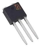
TO-220AB
A
G
A
K
Available either in sensitive (TS8) or standard (TN8 / TYN) gate triggering levels, the
8 A SCR series is suitable to fit all modes of control found in applications such as
overvoltage crowbar protection, motor control circuits in power tools and kitchen aids,
inrush current limiting circuits, capacitive discharge ignition and voltage regulation
circuits.
Available in through-hole or surface-mount packages, they provide an optimized
performance in a limited space.
A
G
Product summary
DPAK
Order code
Voltage (x00)
VDRM/VRRM
600 V
800 V
Sensitivity
IGT
Package
TS820-600B
X
0.2 mA
DPAK
Product status link
TS820-600H
X
0.2 mA
IPAK
TN805, TN815, TS820, TYN608
TS820-600T
X
0.2 mA
TO-220AB
TS820-600FP
X
0.2 mA
TO-220FPAB
TN805-600B
X
5 mA
DPAK
TN815-x00B
X
X
15 mA
DPAK
X
15 mA
IPAK
15 mA
TO-220AB
TN815-800H
TYN608RG
DS2118 - Rev 9 - November 2021
For further information contact your local STMicroelectronics sales office.
X
www.st.com
�TN805, TN815, TS820, TYN608
Characteristics
1
Characteristics
Table 1. Absolute ratings (limiting values)
Value
Symbol
TN805
Parameters
TN815
TYN608
Unit
TS820
IT(RMS)
RMS on-state current On-state rms current
(180° conduction angle)
TO-220FPAB, TC = 91 °C
IT(AV)
Average on-state current (180° conduction angle)
ITSM
Non repetitive surge peak on-state
current
I2t
dl/dt
IGM
PG(AV)
Tstg
Tj
VRGM
TC = 110 °C
tp = 8.3 ms
tp = 10 ms
TC = 110 °C
TO-220FPAB, TC = 91 °C
Tj = 25 °C
8
A
5
A
73
100
70
95
24.5
45
A
tp = 10 ms
Tj = 25 °C
F = 60 Hz
Tj = 125 °C
50
A/µs
tp = 20 µs
Tj = 125 °C
4
A
Tj = 125 °C
1
W
Storage junction temperature range
-40 to +150
°C
Operating junction temperature range
-40 to +125
°C
5
V
I2t value for fusing
Critical rate of rise of on-state current
IG = 2 x IGT , tr ≤ 100 ns
Peak gate current
Average gate power dissipation
Maximum peak reverse gate voltage (for TN8x5 and TYN608 only)
A2s
Table 2. Sensitive electrical characteristics (Tj = 25 °C, unless otherwise specified)
Symbol
IGT
VGT
VD = 12 V, RL = 140 Ω
VRG
IRG = 10 µA
VGD
VD = VDRM, RL = 3.3 kΩ, RGK = 220 Ω
Tj = 125 °C
TS820
Unit
Max.
200
µA
Max.
0.8
V
Min.
8
V
Min.
0.1
V
IH
IT = 50 mA, RGK = 1 kΩ
Max.
5
mA
IL
IG = 1mA, RGK = 1 kΩ
Max.
6
mA
dV/dt
VD = 65% VDRM, RGK = 220 Ω
Tj = 125 °C
Min.
5
V/µs
VTM
ITM = 16 A, tp = 380 μs
Tj = 25 °C
Max.
1.6
V
Vt0
Threshold voltage
Tj = 125 °C
Max.
0.85
V
Rd
Dynamic resistance
Tj = 125 °C
Max.
46
mΩ
5
µA
1
mA
IDRM
IRRM
DS2118 - Rev 9
Parameter
VDRM = VRRM, RGK = 220 Ω
Tj = 25 °C
Tj = 125 °C
Max.
page 2/20
�TN805, TN815, TS820, TYN608
Characteristics
Table 3. Standard electrical characteristics (Tj = 25 °C, unless otherwise specified)
Symbol
IGT
Parameter
VD = 12 V, RL = 140 Ω
VGT
Tj = 125 °C
TN805
TN815
TYN608
Min.
0.5
2
2
Max.
5
15
15
Unit
mA
Max.
1.3
V
Min.
0.2
V
VGD
VD = VDRM, RL = 3.3 kΩ
IH
IT = 100 mA, gate open
Max.
25
40
30
mA
IL
IG = 1.2 IGT
Max.
30
50
70
mA
50
150
150
V/µs
dV/dt
VD = 67% VDRM, gate open
Tj = 125 °C
Min.
VTM
ITM = 16 A, tp = 380 μs
Tj = 25 °C
Max.
1.6
V
Vt0
Threshold voltage
Tj = 125 °C
Max.
0.85
V
Rd
Dynamic resistance
Tj = 125 °C
Max.
46
mΩ
5
µA
2
mA
IDRM
IRRM
Tj = 25 °C
VDRM = VRRM
Tj = 125 °C
Max.
Table 4. Thermal resistance (maximum values)
Symbol
Rth(j-c)
Parameter
Junction to case (DC)
Junction to ambient
Rth(j-a)
Value
Junction to ambient
S(1) = 0.5 cm²
IPAK / DPAK /
TO-220AB
1.3
TO-220FPAB
4.6
DPAK
70
TO-220AB /
TO-220FPAB
60
IPAK
100
Unit
°C/W
°C/W
1. S = Copper surface under tab
DS2118 - Rev 9
page 3/20
�TN805, TN815, TS820, TYN608
Characteristics (curves)
1.1
Characteristics curves
Figure 1. Maximum average power dissipation versus
average on-state current
Figure 2. Average and DC on-state current versus case
temperature
IT(AV) (A)
P(W)
8
10
7
DPAK IPAK
9
α = 180°
TO-220AB
D.C.
8
6
7
5
6
4
α = 180°
5
4
3
360°
TO-220FPAB
3
2
2
1
α
IT(AV) (A)
0
Tcase (°C)
1
0
0
1
3
2
5
4
6
0
25
50
75
100
125
Figure 3. Average and DC on-state current versus ambient Figure 4. Relative variation of thermal impedance junction
temperature
to case versus pulse duration
2.5
IT(AV) (A)
K=[Z th(j-c) /Rth(j-c) ]
1.0
Recommendedpad layout,
FR4 printed circuit board
D.C.
α = 180°
2.0
0.5
TO-220AB
TO-220FPAB
1.5
1.0
0.2
DPAK
IPAK
0.5
Tamb(°C)
0.0
0
25
50
75
tp(s)
0.1
100
125
Figure 5. Relative variation of thermal impedance junction
to ambient versus pulse duration
1E-3
1E-2
1E+0
1E-1
Figure 6. Relative variation of gate trigger current and
holding current versus junction temperature for TS820
IGT,IH ,IL [T j ] / IGT,IH ,IL [T j =25°C]
K=[Z th(j-a) /Rth(j-a) ]
2.0
1.00
Recommended pad layout,
FR4 printed circuit board
1.8
IGT
1.6
1.4
DPAK
1.2
0.10
1.0
IH & I L
R GK = 1kΩ
0.8
TO-220AB / IPAK
TO-220FPAB
0.6
0.4
1E-2
DS2118 - Rev 9
0.2
tp(s)
0.01
1E-1
1E+0
1E+1
1E+2
5E+2
0.0
-40
Tj(°C)
-20
0
20
40
60
80
100
120
140
page 4/20
�TN805, TN815, TS820, TYN608
Characteristics (curves)
Figure 7. Relative variation of gate trigger current and
holding current versus junction temperature
Figure 8. Relative variation of holding current versus
gate-cathode resistance (typical values)
IH[R GK ] / IH[ RGK =1kΩ]
IGT,IH,IL [ Tj ] / IGT,IH,IL [T j =25°C]
6.0
2.4
5.5
2.2
TN8 and TYNx8
IGT
2.0
Tj = 25°C
TS8
5.0
1.8
4.5
1.6
4.0
3.5
1.4
1.2
3.0
IH & IL
1.0
2.5
0.8
2.0
0.6
1.5
1.0
0.4
0.5
Tj(°C)
0.2
0.0
-40
-20
0
20
40
60
80
100
120
140
Figure 9. Relative variation of dV/dt immunity versus gatecathode resistance (typical values) for TS820
dV/dt[R GK ] / dV/dt[ RGK =220Ω]
RGK (kΩ)
0.0
1E-2
1E-1
1E+0
1E+1
Figure 10. Relative variation of dV/dt immunity versus
gate-cathode capacitance (typical values) for TS820
dV/dt[C GK ] / dV/dt[R GK =220Ω]
15.0
10.00
VD = 0.67 x VDRM
Tj = 125°C
RGK = 220Ω
T j = 125°C
V D = 0.67 x V DRM
12.5
1.00
10.0
7.5
0.10
5.0
2.5
R GK(k Ω)
0.01
0
200
400
600
800
1000
1200
1400
1600
1800
2000
CGK(nF)
0.0
0
Figure 11. Surge peak on-state current versus number of
cycles
20
40
60
80
100
120
140
160
180
200
220
Figure 12. Non-repetitive surge peak on-state current and
corresponding values of I2t
ITSM(A)
ITSM(A), I 2t (A 2s)
100
1000
Tj initial = 25°C
90
80
tp=10ms
TYN08
70
ITSM
One cycle
TYN08
Non repetitive
Tj initial=25°C
60
dI/dt limitation
TN8 / TS8
50
100
Sinusoidal pulse width tp < 10 ms
TN8 / TS8
40
TYN08
30
Repetitive
TC=110°C
20
I2t
TN8 / TS8
10
Number ofcycles
0
1
DS2118 - Rev 9
10
100
t p(ms)
10
1000
0.01
0.10
1.00
10.00
page 5/20
�TN805, TN815, TS820, TYN608
Characteristics (curves)
Figure 13. On-state characteristics (maximum values)
Figure 14. Thermal resistance junction to ambient versus
copper surface under tab
ITM(A)
50.0
100
Tj max.:
Vt0 = 0.85 V
Rd = 46 mΩ
Rth(j-a) (°C/W)
DPAK
Epoxy printed circuit board, copper thickness: 35 µm
90
10.0
80
70
Tj=max
60
50
1.0
40
Tj=25°C
30
20
VTM(V)
0.1
0.0
DS2118 - Rev 9
10
SCu (cm²)
0
0.5
1.0
1.5
2.0
2.5
3.0
3.5
4.0
0
5
10
15
20
25
30
35
40
page 6/20
�TN805, TN815, TS820, TYN608
Package information
2
Package information
In order to meet environmental requirements, ST offers these devices in different grades of ECOPACK packages,
depending on their level of environmental compliance. ECOPACK specifications, grade definitions and product
status are available at: www.st.com. ECOPACK is an ST trademark.
2.1
DPAK package information
•
•
Molding compouned resin is halogen free and meets UL94 flammability standard, level V0
Lead-free package leads plating
A
Figure 15. DPAK package outline
E
b4
H
D
D1
L2
c2
e
L4
A1
b
E1
c
e1
A2
V2
L
DS2118 - Rev 9
page 7/20
�TN805, TN815, TS820, TYN608
DPAK package information
Table 5. DPAK package mechanical data
Dimensions
Inches(1)
Millimeters
Ref.
Min.
Typ.
Max.
Min.
Typ.
Max.
A
2.18
2.40
0.0858
0.0945
A1
0.90
1.10
0.0354
0.0433
A2
0.03
0.23
0.0012
0.0091
b
0.64
0.90
0.0252
0.354
b4
4.95
5.46
0.1949
0.2150
c
0.46
0.61
0.0181
0.0240
c2
0.46
0.60
0.0181
0.0236
D
5.97
6.22
0.2350
0.2449
D1
4.95
5.60
0.1949
0.2205
E
6.35
6.73
0.2500
0.2650
E1
4.32
5.50
0.1701
0.2165
e
2.286
0.0900
e1
4.40
4.70
0.1732
0.1850
H
9.35
10.40
0.3681
0.4094
L
1.00
1.78
0.0394
0.0701
L2
1.27
0.0500
L4
0.60
1.02
0.0236
0.0402
V2(2)
-8°
+8°
-8°
+8°
1. Dimensions in inches are given for reference only
2. Degree
Note:
This package drawing may slightly differ from the physical package. However, all the specified dimensions are
guaranteed.
Figure 16. DPAK recommended footprint (dimensions are in mm)
12.7
6.7
3.0
3.0
4.572
6.7
B
The device must be positioned within
DS2118 - Rev 9
A
1.6
0.05 A B
page 8/20
�TN805, TN815, TS820, TYN608
IPAK package information
2.2
IPAK package information
•
•
Molding compouned resin is halogen free and meets UL94 flammability standard, level V0
Lead-free package leads plating
Figure 17. IPAK package outline
E
b4
A
c2
V1
L2
1.20 ±0.010
Top E-MARK
D
L1
A1
e
b2
b
e1
DS2118 - Rev 9
H
L
c
page 9/20
�TN805, TN815, TS820, TYN608
IPAK package information
Table 6. IPAK package mechanical data
Dimensions
MillimetersInches (for reference only)
Ref.
Min.
Typ.
Min.
0.086
A
2.20
2.40
A1
0.90
1.10
b
0.64
0.90
b2
b4
5.20
5.43
c
0.45
0.60
c2
0.46
0.60
D
6
6.20
E
6.40
6.70
e1
Typ.
0.035
0.025
0.035
0.037
0.252
2.28
4.40
H
Max.
0.094
0.95
e
0.263
0.090
4.60
0.173
16.10
0.181
0.634
L
9
9.60
0.354
0.377
L1
0.8
1.20
0.031
0.047
L2
V1
DS2118 - Rev 9
Max.
0.80
10°
1.25
0.031
0.049
10°
page 10/20
�TN805, TN815, TS820, TYN608
TO-220AB package information
2.3
TO-220AB package information
•
•
•
•
•
Molding compouned resin is halogen free and meets UL94 flammability standard, level V0
Lead-free package leads plating
Cooling method: by conduction (C)
Recommended torque value: 0.55 N·m
Maximum torque value: 0.70 N·m
Figure 18. TO-220AB package outline
DS2118 - Rev 9
page 11/20
�TN805, TN815, TS820, TYN608
TO-220AB package information
Table 7. TO-220AB package mechanical data
Dimensions
Millimeters
Ref.
Min.
Max.
Min.
Max.
A
4.40
4.60
0.173
0.181
b
0.61
0.88
0.240
0.035
b1
1.14
1.55
0.045
0.061
c
0.48
0.70
0.019
0.028
D
15.25
15.75
0.600
D1
DS2118 - Rev 9
Inches (for reference only)
1.27 typ.
0.620
0.050 typ.
E
10.00
10.40
0.394
0.409
e
2.40
2.70
0.094
0.106
e1
4.95
5.15
0.195
0.203
F
1.23
1.32
0.048
0.052
H1
6.20
6.60
0.244
0.260
J1
2.40
2.72
0.094
0.107
L
13.00
14.00
0.512
0.551
L1
3.50
3.93
0.138
0.155
L20
16.40 typ.
0.646 typ.
L30
28.90 typ.
1.138 typ.
θP
3.75
3.85
0.148
0.152
Q
2.65
2.95
0.104
0.116
page 12/20
�TN805, TN815, TS820, TYN608
TO-220AB package information
2.4
TO-220AB package information
•
•
•
Molding compound resin is halogen free and meets UL94 flammability standard, level V0
Lead-free plating package leads
Recommended torque: 0.4 to 0.6 N·m
Figure 19. TO-220AB package outline
DS2118 - Rev 9
page 13/20
�TN805, TN815, TS820, TYN608
TO-220AB package information
Table 8. TO-220AB package mechanical data
Dimensions
Min.
A
Inches(1)
Millimeters
Ref.
Typ.
15.20
a1
Max.
Min.
15.90
0.5984
3.75
Typ.
Max.
0.6260
0.1476
a2
13.00
14.00
0.5118
0.5512
B
10.00
10.40
0.3937
0.4094
b1
0.61
0.88
0.0240
0.0346
b2
1.23
1.32
0.0484
0.0520
C
4.40
4.60
0.1732
0.1811
c1
0.49
0.70
0.0193
0.0276
c2
2.40
2.72
0.0945
0.1071
e
2.40
2.70
0.0945
0.1063
F
6.20
6.60
0.2441
0.2598
I
3.73
3.88
0.1469
0.1528
L
2.65
2.95
0.1043
0.1161
I2
1.14
1.70
0.0449
0.0669
I3
1.14
1.70
0.0449
0.0669
I4
15.80
16.80
0.6220
M
16.40
2.6
0.6457
0.6614
0.1024
1. Inch dimensions are for reference only.
DS2118 - Rev 9
page 14/20
�TN805, TN815, TS820, TYN608
TO-220FPAB package information
2.5
TO-220FPAB package information
•
•
Epoxy meets UL94, V0
Recommended torque: 0.4 to 0.6 N·m
Figure 20. TO-220FPAB package outline
DS2118 - Rev 9
page 15/20
�TN805, TN815, TS820, TYN608
TO-220FPAB package information
Table 9. TO-220FPAB package mechanical data
Dimensions
Millimeters
Ref.
Min.
Max.
Min.
Max.
A
4.40
4.60
0.1739
0.1818
B
2.5
2.7
0.0988
0.1067
D
2.50
2.75
0.0988
0.1087
E
0.45
0.70
0.0178
0.0277
F
0.75
1.0
0.0296
0.0395
F1
1.15
1.70
0.0455
0.0672
F2
1.15
1.70
0.0455
0.0672
G
4.95
5.20
0.1957
0.2055
G1
2.40
2.70
0.0949
0.1067
H
10.00
10.40
0.3953
0.4111
L2
DS2118 - Rev 9
Inches
16.00 typ.
0.6324 typ.
L3
28.60
30.60
1.1304
1.2095
L4
9.80
10.6
0.3874
0.4190
L5
2.90
3.60
0.1146
0.1423
L6
15.90
16.40
0.6285
0.6482
L7
9.00
9.30
0.3557
0.3676
Dia
3.0
3.20
0.1186
0.1265
page 16/20
�TN805, TN815, TS820, TYN608
Ordering information
3
Ordering information
Figure 21. TN8 series
TN 8 05 - 600 B -TR
Standard SCR series
Current
8=8A
Sensitivity
05 = 5 mA
15 = 15 mA
Voltage
600 = 600 V
800 = 800 V
Package
B = DPAK
H = IPAK
Packing mode
Blank = Tube
-TR = Tape and reel
Figure 22. TS8 series
TS 8 20 - 600 B (-TR)
Sensitive SCR series
Current
8=8A
Sensitivity
20 = 200 µA
Voltage
600 = 600 V
Package
B = DPAK
H = IPAK
T = TO-220AB
FP = TO220FPAB
Packing mode
Blank = Tube
-TR = Tape and reel
Figure 23. TYNx08 series
TYN
6
08
RG
Standard SCR series
Voltage
6 = 600 V
Current
8=8A
Packing mode
RG = Tube
DS2118 - Rev 9
page 17/20
�TN805, TN815, TS820, TYN608
Ordering information
Table 10. Ordering information
DS2118 - Rev 9
Order code
Marking
Package
Weight
Base qty
Delivery mode
TN805-600B-TR
TN805600
DPAK
0.3 g
2500
Tape and reel
TN815-600B-TR
TN815600
DPAK
0.3 g
2500
Tape and reel
TN815-800B-TR
TN815800
DPAK
0.3 g
2500
Tape and reel
TN815-800H
TN815800
IPAK
0.4 g
75
Tube
TS820-600B
TS820600
DPAK
0.3 g
75
Tube
TS820-600B-TR
TS820600
DPAK
0.3 g
2500
Tape and reel
TS820-600H
TS820600
IPAK
0.4 g
75
Tube
TS820-600T
TS820600T
TO-220AB
2.3 g
50
Tube
TS820-600FP
TS820600
TO-220FPAB
2.0 g
50
Tube
TYN608RG
TYN608
TO-220AB
2.3 g
50
Tube
page 18/20
�TN805, TN815, TS820, TYN608
Revision history
Table 11. Document revision history
DS2118 - Rev 9
Date
Revision
Changes
Apr-2002
4A
13-Feb-2006
5
TO-220AB delivery mode changed from bulk to tube. ECOPACK statement
added.
22-Jan-2010
6
Alpha definition updated in Figure 1. Thermal resistance, junction to case,
updated in Table 5.
10-Oct-2011
7
Added TO-220FPAB package. Removed 700 V and 1000 V products.
14-May-2014
8
Updated DPAK and IPAK package information and reformatted to current
standard.
03-Nov-2021
9
Added TN815-800H product information. Minor text changes.
Last update.
page 19/20
�TN805, TN815, TS820, TYN608
IMPORTANT NOTICE – PLEASE READ CAREFULLY
STMicroelectronics NV and its subsidiaries (“ST”) reserve the right to make changes, corrections, enhancements, modifications, and improvements to ST
products and/or to this document at any time without notice. Purchasers should obtain the latest relevant information on ST products before placing orders. ST
products are sold pursuant to ST’s terms and conditions of sale in place at the time of order acknowledgement.
Purchasers are solely responsible for the choice, selection, and use of ST products and ST assumes no liability for application assistance or the design of
Purchasers’ products.
No license, express or implied, to any intellectual property right is granted by ST herein.
Resale of ST products with provisions different from the information set forth herein shall void any warranty granted by ST for such product.
ST and the ST logo are trademarks of ST. For additional information about ST trademarks, please refer to www.st.com/trademarks. All other product or service
names are the property of their respective owners.
Information in this document supersedes and replaces information previously supplied in any prior versions of this document.
© 2021 STMicroelectronics – All rights reserved
DS2118 - Rev 9
page 20/20
�