TS331, TS332, TS334
Micropower low-voltage, rail-to-rail comparators
Datasheet - production data
Applications
TS331 (single)
• Mobile phones
• Notebooks and PDAs
• Battery-supplied electronics
• General-purpose portable devices
SOT23-5/SC70-5
• General-purpose low voltage applications
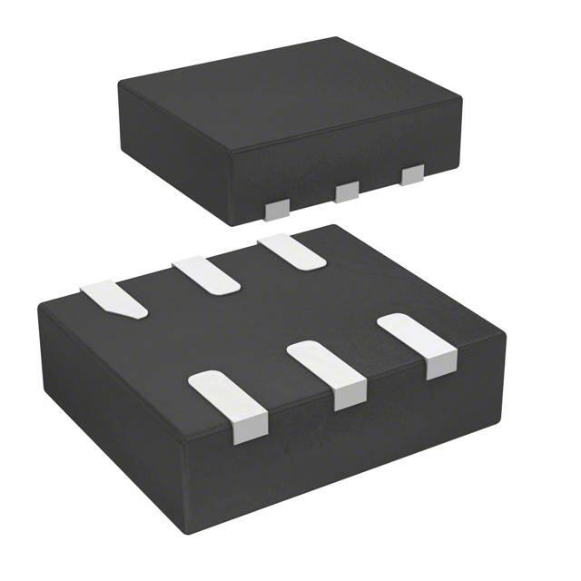
DFN6 1.2x1.3
Description
TS332 (dual)
SO8
DFN8 2x2
MiniSO8
The TS331, TS332 and TS334 are single, dual
and quad micropower and low-voltage
comparators. They can operate with a supply
voltage ranging from 1.6 V to 5 V with a typical
current consumption as low as 20 µA. In addition,
rail-to-rail inputs make them a perfect choice for
low-voltage applications.
Their availability in tiny packages is a real
advantage for overcoming space constraints.
TS334 (quad)
The TS33x are specified for temperatures
between -40 °C to +125 °C, making them ideal for
a wide range of applications.
QFN16 3x3
SO14
TSSOP14
Features
• Supply operation from 1.6 V to 5 V
• Low current consumption: 20 µA
• Rail-to-rail inputs
• Wide temperature range: -40 °C to +125 °C
• Low output saturation voltage
• Low propagation delay: 210 ns
• Open-drain output
• ESD tolerance: 2 kV HBM/200 V MM
• SMD packages
• Automotive qualified
January 2022
This is information on a product in full production.
DocID17272 Rev 5
1/27
www.st.com
27
�Contents
TS331, TS332, TS334
Contents
1
Package pin connections . . . . . . . . . . . . . . . . . . . . . . . . . . . . . . . . . . . . . 3
2
Absolute maximum ratings and operating conditions . . . . . . . . . . . . . 4
3
Electrical characteristics . . . . . . . . . . . . . . . . . . . . . . . . . . . . . . . . . . . . . 6
4
Package information . . . . . . . . . . . . . . . . . . . . . . . . . . . . . . . . . . . . . . . . 13
4.1
SOT23-5 package information . . . . . . . . . . . . . . . . . . . . . . . . . . . . . . . . . 14
4.2
SC70-5 (SOT323-5) package information . . . . . . . . . . . . . . . . . . . . . . . . 15
4.3
DFN6 1.2x1.3 package information . . . . . . . . . . . . . . . . . . . . . . . . . . . . . 16
4.4
DFN8 2x2 package information . . . . . . . . . . . . . . . . . . . . . . . . . . . . . . . . 17
4.5
SO8 package information . . . . . . . . . . . . . . . . . . . . . . . . . . . . . . . . . . . . . 19
4.6
MiniSO8 package information . . . . . . . . . . . . . . . . . . . . . . . . . . . . . . . . . 20
4.7
QFN16 3x3 package information . . . . . . . . . . . . . . . . . . . . . . . . . . . . . . . 21
4.8
SO14 package information . . . . . . . . . . . . . . . . . . . . . . . . . . . . . . . . . . . . 23
4.9
TSSOP14 package information . . . . . . . . . . . . . . . . . . . . . . . . . . . . . . . . 24
5
Ordering information . . . . . . . . . . . . . . . . . . . . . . . . . . . . . . . . . . . . . . . 25
6
Revision history . . . . . . . . . . . . . . . . . . . . . . . . . . . . . . . . . . . . . . . . . . . 26
2/27
DocID17272 Rev 5
�TS331, TS332, TS334
Package pin connections
Figure 1. Pin connections for each package (top view)
,1�
�
9&&�
�
,1�
�
�
�
287
TS331
SOT23-5/SC70-5
287�
�
,1��
�
,1��
�
9&&�
�
1&
���
287�
287�
287�
287�
��
��
��
�
�
9&&��
9&&��
�
�
1& ���
,1��
�
�
,1��
TS331
DFN6 1.2x1.3
�
9&&�
287�
9&&�
�
287�
,1��
287�
�
,1��
,1��
,1��
�
,1��
9&&�
,1��
TS332
DFN8 2x2
��
287
9&&�
TS332
SO8/MiniSO8
OUT2
1
14
OUT3
OUT1
2
13
OUT4
��
9&&�
VCC+
3
12
VCC-
��
,1��
IN1-
4
11
IN4+
�
��
1&
5
10
IN4-
�
,1��
IN1+
�
�
1&
,1��
1&���
�
�
�
�
IN2-
6
9
IN3+
,1��
,1��
,1��
�
,1��
9&&�
,1��
1
Package pin connections
IN2+
7
8
IN3-
TS334
QFN16 3x3
TS334
SO14/TSSOP14
1. NC = not connected
2. The exposed pads of the DFN8 2x2 and the QFN16 3x3 can be connected to VCC- or left floating.
DocID17272 Rev 5
3/27
�Absolute maximum ratings and operating conditions
2
TS331, TS332, TS334
Absolute maximum ratings and operating conditions
Table 1. Absolute maximum ratings
Symbol
Parameter
VCC
Supply voltage(1)
VID
Differential input voltage
VIN
Input voltage range
Vout
Output voltage(1)
Rthja
Value
5.5
± 5.5
(VCC-) - 0.3 to (VCC+) + 0.3
5.5
Thermal resistance junction to ambient
SOT23-5
SC70-5
DFN6 1.2x1.3
DFN8 2x2
SO8
MiniSO8
QFN16 3x3
SO14
TSSOP14
Storage temperature
-65 to +150
Tj
Junction temperature
150
Lead temperature (soldering 10 seconds)
260
(HBM)(3)
Machine model (MM)
°C/W
(2)
Tstg
Human body model
(4)
81
172
40
39
5
31
32
200
1500
Latchup immunity
200
2. Short-circuits can cause excessive heating. These values are typical
3. According to JEDEC standard JESD22-A114F.
4. According to JEDEC standard JESD22-A115A.
5. According to ANSI/ESD STM5.3.1.
DocID17272 Rev 5
°C
2000
Charged device model (CDM)(5)
1. All voltage values, except differential voltage, are referenced to Vcc-
4/27
250
205
40
57
125
190
39
105
100
Rthjc
ESD
V
(2)
Thermal resistance junction to case
SOT23-5
SC70-5
SO8
MiniSO8
QFN16 3x3
SO14
TSSOP14
TLEAD
Unit
V
mA
�TS331, TS332, TS334
Absolute maximum ratings and operating conditions
Table 2. Operating conditions
Symbol
Parameter
Toper
Operating temperature range
VCC
Supply voltage (VCC+) - (VCC-)
-40°C < Tamb < +125°C
VICM
Common mode input voltage range
Tamb = +25°C
-40°C < Tamb < +125°C
DocID17272 Rev 5
Value
Unit
-40 to +125
°C
1.6 to 5.0
V
(VCC-) - 0.2 to (VCC+) + 0.2
(VCC-) to (VCC+)
5/27
�Electrical characteristics
3
TS331, TS332, TS334
Electrical characteristics
Table 3. VCC+ = +1.8 V, VCC- = 0 V, Tamb = +25°C (unless otherwise specified)
Symbol
VIO
Parameter
Input offset voltage
∆Vio/∆T Input offset voltage drift
IIB
IIO
Input bias current(1)
Input offset
current(1)
Test conditions
Min.
Supply current
Max.
0.5
5
-40 °C < Tamb < +125 °C
6
-40 °C < Tamb < +125 °C
25
-40°C < Tamb < +125 °C
-40°C < Tamb < +125 °C
Output current leakage
VOL
Output voltage low
ISINK
Output sink current
CMRR Common mode rejection ratio
TPHL
TPLH
delay(2)
Propagation
High to low output level
Propagation delay(3)
Low to high output level
10
nA
100
20
-40 °C < Tamb < +125 °C
26
30
No load, output high, VICM = 0 V
22
-40 °C < Tamb < +125 °C
IOH
mV
40
100
1
Unit
µV/°C
4.5
No load, output low, VICM = 0 V
ICC
Typ.
29
µA
33
VOUT = VCC+
1
-40 °C < Tamb < +125 °C
10
500
ISINK = 1 mA
24
-40 °C < Tamb < +125 °C
30
50
VOUT = 1.5 V
20
-40°C < Tamb < +125°C
15
0 < VICM < 1.8 V
50
22
300
VICM = 0 V, RL = 5.1 kΩ, CL = 50 pF,
overdrive = 100 mV
210
VICM = 0 V, RL = 5.1 kΩ, CL = 50 pF,
overdrive = 10 mV
540
VICM = 0 V, RL = 5.1 kΩ, CL = 50 pF,
overdrive = 100 mV
420
mV
mA
68
VICM = 0 V, RL = 5.1 kΩ, CL = 50 pF,
overdrive = 10 mV
nA
dB
310
ns
620
1. Maximum values include unavoidable inaccuracies of the industrial tests.
2. TPHL is measured when the output signal crosses a voltage level at 50% of Vcc with the following conditions: inverting input
voltage (IN-) = VICM and non-inverting input voltage (IN+) moving from VICM + 100 mV to VICM - overdrive.
3. TPLH is measured when the output signal crosses a voltage level at 50% of Vcc with the following conditions: inverting input
voltage (IN-) = VICM and non-inverting input voltage (IN+) moving from VICM - 100 mV to VICM + overdrive.
6/27
DocID17272 Rev 5
�TS331, TS332, TS334
Electrical characteristics
Table 4. VCC+ = +2.7 V, VCC- = 0 V, Tamb = +25°C (unless otherwise specified)
Symbol
VIO
Parameter
Input offset voltage
∆Vio/∆T Input offset voltage drift
IIB
IIO
Input bias current(1)
Test conditions
Min.
Supply current
0.5
5
6
-40 °C < Tamb < +125 °C
25
-40 °C < Tamb < +125 °C
-40 °C < Tamb < +125 °C
Output current leakage
VOL
Output voltage low
ISINK
Output sink current
CMRR Common mode rejection ratio
TPHL
TPLH
Propagation delay(2)
High to low output level
Propagation delay(3)
Low to high output level
10
nA
100
21
-40 °C < Tamb < +125 °C
27
31
No load, output high, VICM = 0 V
23
-40°C < Tamb < +125 °C
IOH
mV
40
100
1
Unit
µV/°C
3.3
No load, output low, VICM = 0 V
ICC
Max.
-40 °C < Tamb < +125 °C
(1)
Input offset current
Typ.
30
µA
34
VOUT = VCC+
1
-40 °C < Tamb < +125 °C
10
500
ISINK = 1 mA
17
-40 °C < Tamb < +125 °C
30
50
VOUT = 1.5 V
40
-40 °C < Tamb < +125 °C
30
0 < VICM < 2.7 V
54
-40 °C < Tamb < +125 °C
53
47
320
VICM = 0 V, RL = 5.1 kΩ,
CL = 50 pF, overdrive = 100 mV
220
VICM = 0 V, RL = 5.1 kΩ, CL = 50 pF,
overdrive = 10 mV
550
VICM = 0 V, RL = 5.1 kΩ, CL = 50 pF,
overdrive = 100 mV
420
mV
mA
74
VICM = 0 V, RL = 5.1 kΩ,
CL = 50 pF, overdrive = 10 mV
nA
dB
320
ns
640
1. Maximum values include unavoidable inaccuracies of the industrial tests.
2. TPHL is measured when the output signal crosses a voltage level at 50% of Vcc with the following conditions: Inverting
input voltage (IN-) = VICM and non-inverting input voltage (IN+) moving from VICM + 100 mV to VICM - overdrive.
3. TPLH is measured when the output signal crosses a voltage level at 50% of Vcc with the following conditions: Inverting
input voltage (IN-) = VICM and non-inverting input voltage (IN+) moving from VICM - 100 mV to VICM + overdrive.
DocID17272 Rev 5
7/27
�Electrical characteristics
TS331, TS332, TS334
Table 5. VCC+ = +5 V, VCC- = 0 V, Tamb = +25°C (unless otherwise specified)
Symbol
VIO
Parameter
Input offset voltage
∆Vio/∆T Input offset voltage drift
IIB
IIO
Input bias current(1)
Input offset current
Test conditions
Min.
0.5
5
6
-40 °C < Tamb < +125 °C
30
-40 °C < Tamb < +125 °C
-40 °C < Tamb < +125 °C
Output current leakage
VOL
Output voltage low
ISINK
Output sink current
AV
23
-40 °C < Tamb < +125 °C
CMRR Common mode rejection ratio
SVR
TPHL
TPLH
Supply voltage rejection
delay(2)
Propagation
High to low output level
Propagation delay(3)
Low to high output level
26
34
VOUT = VCC+
1
-40 °C < Tamb < +125 °C
10
600
ISINK = 1 mA
48
-40 °C < Tamb < +125 °C
60
80
VOUT = 1.5 V
82
-40 °C < Tamb < +125 °C
60
93
40
100
0 < VICM < 5 V
60
79
-40 °C < Tamb < +125 °C
58
∆VCC = 1.8 to 5 V
56
-40 °C < Tamb < +125 °C
56
380
VICM = 0 V, RL = 5.1 kΩ, CL = 50 pF,
overdrive = 100 mV
270
VICM = 0 V, RL = 5.1 kΩ, CL = 50 pF,
overdrive = 10 mV
570
VICM = 0 V, RL = 5.1 kΩ, CL = 50 pF,
overdrive = 100 mV
450
nA
mV
mA
V/mV
dB
75
VICM = 0 V, RL = 5.1 kΩ, CL = 50 pF,
overdrive = 10 mV
430
ns
720
2. TPHL is measured when the output signal crosses a voltage level at 50% of Vcc with the following conditions: Inverting
input voltage (IN-) = VICM and non-inverting input voltage (IN+) moving from VICM + 100 mV to VICM - overdrive.
3. TPLH is measured when the output signal crosses a voltage level at 50% of Vcc with the following conditions: Inverting
input voltage (IN-) = VICM and non-inverting input voltage (IN+) moving from VICM - 100 mV to VICM + overdrive.
DocID17272 Rev 5
µA
38
1. Maximum values include unavoidable inaccuracies of the industrial tests.
8/27
nA
30
34
No load, output high, VICM = 0 V
Voltage gain
10
100
-40 °C < Tamb < +125 °C
IOH
mV
40
100
1
Unit
µV/°C
1.3
(1)
Supply current
Max.
-40 °C < Tamb < +125 °C
No load, output low, VICM = 0 V
ICC
Typ.
�TS331, TS332, TS334
Electrical characteristics
Figure 2. Supply current versus supply voltage Figure 3. Supply current versus supply voltage
with output high, VICM = 0 V
with output high, VICM = VCC
34
28
V
ICM
=0V
( A)
( A)
ICM
24
CC
o
T = -40 C
o
T = 25 C
16
CC
o
T = 125 C
30
Supply current I
20
= V
Output HIGH
T = 125 C
CC
Supply current I
V
32
o
Output HIGH
28
26
o
T = 25 C
24
22
o
T = -40 C
20
12
18
1.6
2.0
2.4
2.8
3.2
3.6
4.0
Supply voltage V
CC
4.4
4.8
1.6
2.0
2.4
2.8
(V)
3.2
3.6
4.0
Supply voltage V
CC
4.4
4.8
(V)
Figure 4. Supply current versus supply voltage Figure 5. Supply current versus supply voltage
with output low, VICM = 0 V
with output low, VICM = VCC
36
28
V
ICM
V
=0V
34
( A)
o
T = 125 C
Supply current I
Supply curent I
20
o
T = - 40 C
o
16
T = 25 C
ICM
= V
CC
Output LOW
o
T = 125 C
32
CC
24
CC
( A)
Output LOW
30
28
o
26
T = 25 C
24
o
T = - 40 C
22
12
20
1.6
2.0
2.4
2.8
3.2
3.6
4.0
Supply voltage V
CC
4.4
1.6
4.8
3.2
3.6
4.0
4.4
4.8
(V)
Figure 7. Input bias current versus input
common-mode voltage
40
V
CC
(uA)
2.8
CC
40
= 5V
30
(nA)
Ouput LOW
No load
Input bias current I
30
V
ICM
20
= V
CC
V
ICM
= 0V
V
CC
= 5V
20
10
IB
CC
2.4
Supply voltage V
Figure 6. Supply current versus temperature
Supply current I
2.0
(V)
0
o
T =125 C
-10
o
T = 25 C
-20
-30
-40
o
-50
T = - 40 C
-60
-40
-20
0
20
40
60
80
100
120
140
Temperature ( C)
-0.5
0.0
0.5
1.0
1.5
2.0
2.5
3.0
3.5
Common mode voltage V
ICM
DocID17272 Rev 5
4.0
4.5
5.0
5.5
(V)
9/27
�Electrical characteristics
TS331, TS332, TS334
Figure 8. Input current versus differential input
voltage
Figure 9. Input offset voltage versus
temperature
10
1.5
CC
V
ICM
(nA)
-10
-20
IN
I
-30
Input current I
= 5V
I
-40
= 0V
o
IN+
I
125 C
o
IN-
125 C
o
IN+
Input offset voltage Vio (mV)
V
0
25 C
I
o
25 C
IN-
-50
-60
I
-70
o
IN+
-40 C
I
o
IN-
-40 C
V
CC
= 5V
1.0
V
ICM
= 0V
V
0.5
ICM
= 5V
-80
-90
-100
0.0
-100
-80
-60
-40
-20
0
20
40
Differential input voltage V
ID
60
80
40
60
80
100
120
140
Figure 11. Output voltage versus output sink
current, VCC = 2.7 V
110
= 1.8V
V
CC
(mV)
V
o
T = 125 C
120
100
100
o
T = 25 C
80
60
o
T = - 40 C
40
= 2.7V
Output LOW
90
OUT
Output LOW
o
T = 125 C
80
Output voltage V
(mV)
OUT
20
120
CC
Output voltage V
0
Temperature ( C)
180
140
-20
(mV)
Figure 10. Output voltage versus output sink
current, VCC = 1.8 V
160
-40
100
70
o
60
T = 25 C
50
40
o
30
T = - 40 C
20
20
10
0
0
0.0
0.5
1.0
1.5
2.0
2.5
3.0
3.5
Output sink current I
SINK
4.0
4.5
5.0
0.0
2.0
2.5
3.0
3.5
SINK
4.0
4.5
5.0
(mA)
V
CC
(mA)
120
= 5V
T = 25°C
100
Output LOW
SINK
Output LOW
60
Output sink Current I
(mV)
OUT
Output voltage V
1.5
Figure 13. Output sink current versus output
voltage
90
70
1.0
Output sink current I
Figure 12. Output voltage versus output sink
current, VCC = 5 V
80
0.5
(mA)
o
T = 125 C
50
o
T = 25 C
40
30
o
T = - 40 C
20
V
CC
= 5V
80
V
60
CC
= 2.7V
40
V
CC
= 1.8V
20
10
0
0.0
0.5
1.0
1.5
2.0
2.5
3.0
Output sink current I
10/27
3.5
SINK
4.0
4.5
5.0
(mA)
0.5
1.0
1.5
2.0
Output voltage V
OUT
DocID17272 Rev 5
(V)
2.5
3.0
�TS331, TS332, TS334
Electrical characteristics
Figure 14. Output voltage versus temperature
Figure 15. Propagation delay versus overdrive
with negative transition, VCC = 1.8 V
400
Output voltage V
SINK
= 5mA
V
CC
140
V
= 2.7V
CC
120
V
100
= 1.8V
CC
80
60
V
CC
40
-40
-20
0
20
40
60
80
HL
o
T = - 40 C
TP
HL
o
T = 125 C
250
120
0
140
10
20
30
60
70
80
OV
90
100
110
(mV)
Figure 17. Propagation delay versus common
mode voltage, VCC = 1.8 V
CC
LH
ICM
LH
= 0V
R = 5.1k
o
600
= 1.8V
V
TP
T = 125 C
Propagation delay TP (ns)
(ns)
50
600
V
650
Propagation delay TP
40
Overdrive voltage V
700
, C = 50pF
L
L
550
TP
LH
500
TP
o
LH
T = -40 C
o
T = 25 C
450
TP
LH
V
TP
500
V
= 100mV
OV
400
TP
HL
V
300
= 20mV
OV
V
200
CC
HL
V
= 100mV
R = 5.1k
0.5
1.0
1.5
L
OV
10
20
30
40
50
60
70
Overdrive voltage V
OV
80
90
100
100
110
0.0
(mV)
= 1.8V
T = 25°C
TP
0
= 20mV
OV
LH
400
Common mode voltage V
ICM
Figure 18. Propagation delay versus overdrive
with negative transition, VCC = 2.7 V
, C = 50pF
L
2.0
(V)
Figure 19. Propagation delay versus overdrive
with positive transition, VCC = 2.7 V
400
V
= 0V
ICM
350
R = 5.1k
TP
L
, C = 50pF
L
HL
o
T = - 40 C
300
TP
HL
o
T = 25 C
V
CC
TP
HL
o
T = 125 C
250
= 2.7V
V
650
ICM
LH
= 2.7V
CC
Propagation delay TP
V
(ns)
700
(ns)
HL
L
200
Figure 16. Propagation delay versus overdrive
with positive transition, VCC = 1.8 V
Propagation delay TP
, C = 50pF
L
TP
Temperature ( C)
350
= 0V
R = 5.1k
o
T = 25 C
300
= 5V
100
ICM
HL
350
= 1.8V
V
TP
HL
OUT
160
(ns)
I
Propagation delay TP
(mV)
180
= 0V
R = 5.1k
TP
, C = 50pF
L
LH
L
o
T = 125 C
600
550
TP
LH
o
500
TP
T = - 40 C
LH
o
T = 25 C
450
200
0
10
20
30
40
50
60
70
Overdrive voltage V
OV
80
90
100
110
400
0
(mV)
10
20
30
40
50
60
70
Overdrive voltage V
OV
DocID17272 Rev 5
80
90
100
110
(mV)
11/27
�Electrical characteristics
TS331, TS332, TS334
Figure 20. Propagation delay versus common
mode voltage, VCC = 2.7 V
Figure 21. Propagation delay versus overdrive
with negative transition, VCC = 5 V
500
TP
LH
LH
= 20mV
V
OV
500
= 100mV
OV
400
TP
TP
HL
V
300
HL
= 20mV
V
OV
V
CC
= 100mV
OV
V
200
CC
= 5V
V
= 0V
ICM
450
HL
V
(ns)
TP
R = 5.1k
, C = 50pF
L
Propagation delay TP
Propagation delay TP (ns)
600
L
TP
HL
o
T = 25 C
400
TP
350
HL
TP
o
T = - 40 C
HL
o
T = 125 C
= 2.7V
300
T = 25°C
R = 5.1k
, C = 50pF
L
L
250
100
-0.5
0.0
0.5
1.0
1.5
2.0
2.5
Common mode voltage V
3.0
20
30
40
50
60
70
OV
80
90
V
LH
ICM
= 0V
R = 5.1k
TP
Propagation delay TP (ns)
CC
650
= 5V
, C = 50pF
L
L
LH
o
T = 125 C
600
550
TP
LH
o
T = -40 C
TP
LH
500
TP
TP
LH
V
LH
= 20mV
V
OV
500
= 100mV
OV
400
300
o
T = 25 C
TP
200
HL
V
V
CC
TP
HL
= 20mV
OV
450
V
= 5V
T = 25°C
= 100mV
R = 5.1k
OV
, C = 50pF
L
0
10
20
30
40
50
60
70
Overdrive voltage V
OV
80
90
100
110
100
0
1
2
(mV)
3
L
4
5
Common mode voltage V
ICM
Figure 24. Propagation delay versus time with
negative transition
6
ICM
R =5.1k
L
=0V
V
OUT
, C =50pF
L
V
T = 25°C
4
(V)
= 5V, V
CC
= 10mV
OUT
V
5
OV
V
3
= 20mV
OV
2
V
= 100mV
50% V
OV
V
OUT
IN
100mV
Output voltage V
(V)
OUT
Output voltage V
(V)
Figure 25. Propagation delay versus time with
positive transition
6
5
V
CC
= 5V, V
ICM
R =5.1k
4
=0V
V
OUT
, C =50pF
L
L
T = 25°C
V
3
V
= 100mV
= 10mV
OV
OV
2
V
= 20mV
50% V
OV
OUT
1
V
IN
0
0
V
V
OV
100mV
TP
OV
-1
-1
HL
TP
LH
-2
-200
-100
0
100
200
300
400
500
-2
Time (ns)
12/27
110
600
V
1
100
(mV)
Figure 23. Propagation delay versus common
mode voltage, VCC = 5 V
700
(ns)
10
Overdrive voltage V
Figure 22. Propagation delay versus overdrive
with positive transition, VCC = 5 V
Propagation delay TP
0
(V)
ICM
0
500
Time (ns)
DocID17272 Rev 5
1000
�TS331, TS332, TS334
4
Package information
Package information
In order to meet environmental requirements, ST offers these devices in different grades of
ECOPACK packages, depending on their level of environmental compliance. ECOPACK
specifications, grade definitions and product status are available at: www.st.com.
ECOPACK is an ST trademark.
DocID17272 Rev 5
13/27
�Package information
4.1
TS331, TS332, TS334
SOT23-5 package information
Figure 26. SOT23-5 package mechanical drawing
Table 6. SOT23-5 package mechanical data
Dimensions
Ref.
A
Inches(1)
Millimeters
Min.
Typ.
Max.
Min.
Typ.
Max.
0.90
1.20
1.45
0.035
0.047
0.057
A1
0.15
A2
0.90
1.05
1.30
0.035
0.041
0.051
B
0.35
0.40
0.50
0.013
0.015
0.019
C
0.09
0.15
0.20
0.003
0.006
0.008
D
2.80
2.90
3.00
0.110
0.114
0.118
D1
1.90
0.075
e
0.95
0.037
E
2.60
2.80
3.00
0.102
0.110
0.118
F
1.50
1.60
1.75
0.059
0.063
0.069
L
0.10
0.35
0.60
0.004
0.013
0.023
K
0°
10°
0°
1. Values in inches are rounded to three decimal digits.
14/27
0.006
DocID17272 Rev 5
10°
�TS331, TS332, TS334
4.2
Package information
SC70-5 (SOT323-5) package information
Figure 27. SC70-5 (SOT323-5) package mechanical drawing
SIDE VIEW
DIMENSIONS IN MM
GAUGE PLANE
COPLANAR LEADS
SEATING PLANE
TOP VIEW
Table 7. SC70-5 (or SOT323-5) package mechanical data
Dimensions
Ref
Min
A
Inches(1)
Millimeters
Typ
0.80
A1
Max
Min
1.10
0.315
Typ
0.043
0.10
A2
0.80
b
0.90
Max
0.004
1.00
0.315
0.035
0.15
0.30
0.006
0.012
c
0.10
0.22
0.004
0.009
D
1.80
2.00
2.20
0.071
0.079
0.087
E
1.80
2.10
2.40
0.071
0.083
0.094
E1
1.15
1.25
1.35
0.045
0.049
0.053
e
0.65
0.025
e1
1.30
0.051
L
0.26
<
0°
0.36
0.46
0.010
8°
0°
0.014
0.039
0.018
8°
1. Values in inches are rounded to three decimal digits.
DocID17272 Rev 5
15/27
�Package information
4.3
TS331, TS332, TS334
DFN6 1.2x1.3 package information
Figure 28. DFN6 1.2x1.3 package mechanical drawing
Table 8. DFN6 1.2x1.3 package mechanical data
Dimensions
Ref
Inches(1)
Millimeters
Min
Typ
Max
Min
Typ
Max
A
0.45
0.50
0.55
0.018
0.020
0.022
A1
0.00
0.02
0.05
0.000
0.001
0.002
b
0.15
0.18
0.25
0.006
0.007
0.002
c
0.05
0.002
D
1.20
0.047
E
1.30
0.051
e
0.4
0.016
L
0.475
0.525
0.575
0.019
0.021
0.023
L3
0.375
0.425
0.475
0.015
0.017
0.019
1. Values in inches are rounded to three decimal digits.
16/27
DocID17272 Rev 5
�TS331, TS332, TS334
4.4
Package information
DFN8 2x2 package information
Figure 29. DFN8 2x2 package mechanical drawing
$06�����B9�
Table 9.
DFN8 2x2x0.6 mm package mechanical data (pitch 0.5 mm)
Dimensions
Ref.
A
Millimeters
Inches
Min.
Typ.
Max.
Min.
Typ.
Max.
0.51
0.55
0.60
0.020
0.022
0.024
A1
0.05
A3
0.002
0.15
0.006
b
0.18
0.25
0.30
0.007
0.010
0.012
D
1.85
2.00
2.15
0.073
0.079
0.085
D2
1.45
1.60
1.70
0.057
0.063
0.067
E
1.85
2.00
2.15
0.073
0.079
0.085
E2
0.75
0.90
1.00
0.030
0.035
0.039
e
0.50
0.020
L
0.425
0.017
ddd
0.08
0.003
DocID17272 Rev 5
17/27
�Package information
TS331, TS332, TS334
Figure 30. DFN8 2x2 footprint recommendation
�����PP
�����PP
�����PP
�����PP
�����PP
�����PP
$06�����B9�
18/27
DocID17272 Rev 5
�TS331, TS332, TS334
4.5
Package information
SO8 package information
Figure 31. SO8 package mechanical drawing
Table 10. SO8 package mechanical data
Dimensions
Ref.
Inches(1)
Millimeters
Min.
Typ.
A
Max.
Min.
Typ.
1.75
0.069
A1
0.10
A2
1.25
b
0.28
0.48
0.011
0.019
c
0.17
0.23
0.007
0.010
D
4.80
4.90
5.00
0.189
0.193
0.197
E
5.80
6.00
6.20
0.228
0.236
0.244
E1
3.80
3.90
4.00
0.150
0.154
0.157
e
0.25
Max.
0.004
0.010
0.049
1.27
0.050
h
0.25
0.50
0.010
0.020
L
0.40
1.27
0.016
0.050
L1
k
ccc
1.04
0
0.040
8°
0.10
1°
8°
0.004
1. Values in inches are rounded to three decimal digits.
DocID17272 Rev 5
19/27
�Package information
4.6
TS331, TS332, TS334
MiniSO8 package information
Figure 32. MiniSO8 package mechanical drawing
Table 11. MiniSO8 package mechanical data
Dimensions
Ref.
Inches(1)
Millimeters
Min.
Typ.
A
Max.
Typ.
1.1
A1
0
A2
0.75
b
Max.
0.043
0.15
0
0.95
0.030
0.22
0.40
0.009
0.016
c
0.08
0.23
0.003
0.009
D
2.80
3.00
3.20
0.11
0.118
0.126
E
4.65
4.90
5.15
0.183
0.193
0.203
E1
2.80
3.00
3.10
0.11
0.118
0.122
e
L
0.85
0.65
0.40
0.60
0.006
0.033
0.80
0.016
0.024
0.95
0.037
L2
0.25
0.010
ccc
0°
0.037
0.026
L1
k
8°
0.10
1. Values in inches are rounded to three decimal digits.
20/27
Min.
DocID17272 Rev 5
0°
0.031
8°
0.004
�TS331, TS332, TS334
4.7
Package information
QFN16 3x3 package information
Figure 33. QFN16 3 x 3 mm package mechanical drawing
*$06����������&%
DocID17272 Rev 5
21/27
�Package information
Table 12.
TS331, TS332, TS334
QFN16 3 x 3 mm package mechanical data (pitch 0.5 mm)
Dimensions
Ref.
Millimeters
Inches
Min.
Typ.
Max.
Min.
Typ.
Max.
A
0.80
0.90
1.00
0.031
0.035
0.039
A1
0
0.05
0
A3
0.20
b
0.18
D
2.90
D2
1.50
E
2.90
E2
1.50
e
L
3.00
3.00
0.008
0.30
0.007
3.10
0.114
1.80
0.059
3.10
0.114
1.80
0.059
0.50
0.30
0.002
0.012
0.118
0.071
0.118
0.122
0.071
0.020
0.50
0.012
0.020
Figure 34. QFN16 3 x 3 mm footprint recommendation
*$06����������
22/27
0.122
DocID17272 Rev 5
�TS331, TS332, TS334
4.8
Package information
SO14 package information
Figure 35. SO14 package mechanical drawing
Table 13. SO14 package mechanical data
Dimensions
Inches(1)
Millimeters
Ref.
Min.
Typ.
Max.
Min.
Typ.
Max.
A
1.35
1.75
0.050
0.068
A1
0.10
0.25
0.004
0.009
A2
1.10
1.65
0.040
0.060
B
0.33
0.51
0.010
0.020
C
0.19
0.25
0.007
0.009
D
8.55
8.75
0.330
0.340
E
3.80
4.0
0.150
0.150
e
1.27
0.05
H
5.80
6.20
0.220
0.240
h
0.25
0.50
0.009
0.020
L
0.40
1.27
0.015
0.050
k
ddd
8° (max.)
0.10
0.004
1. Values in inches are rounded to three decimal digits.
DocID17272 Rev 5
23/27
�Package information
4.9
TS331, TS332, TS334
TSSOP14 package information
Figure 36. TSSOP14 package mechanical drawing
Table 14. TSSOP14 package mechanical data
Dimensions
Ref.
Inches(1)
Millimeters
Min.
Typ.
A
Max.
Typ.
1.20
A1
0.05
A2
0.80
b
Max.
0.047
0.15
0.002
0.004
0.006
1.05
0.031
0.039
0.041
0.19
0.30
0.007
0.012
c
0.09
0.20
0.004
0.0089
D
4.90
5.00
5.10
0.193
0.197
0.201
E
6.20
6.40
6.60
0.244
0.252
0.260
E1
4.30
4.40
4.50
0.169
0.173
0.176
e
L
k
aaa
1.00
0.65
0.45
L1
0.60
0.0256
0.75
0.018
1.00
0°
0.024
0.030
0.039
8°
0.10
1. Values in inches are rounded to three decimal digits.
24/27
Min.
DocID17272 Rev 5
0°
8°
0.004
�TS331, TS332, TS334
5
Ordering information
Ordering information
Table 15. Order codes
Order code
Temperature range
TS331ILT
Package
Packaging
Marking
K506
SOT23-5
(1)
TS331IYLT
K513
TS331ICT
SC70-5
K55
TS331IQT
DFN6 1.2x1.3
K3
TS332IQ2T
DFN8 2x2
K55
TS332IDT
TS332IYDT(1)
TS332IST
TS334IQ4T
TS334IDT
TS334IYDT(1)
TS334IPT
TS334IYPT(1)
-40 °C, +125 °C
SO8
332I
Tape and reel
332IY
MiniSO8
K507
QFN16 3x3
K307
SO14
TSSOP14
334I
334IY
334I
334IY
1. Qualified and characterized according to AEC Q100 and Q003 or equivalent, advanced screening
according to AEC Q001 and Q 002 or equivalent.
DocID17272 Rev 5
25/27
�Revision history
6
TS331, TS332, TS334
Revision history
Table 16. Document revision history
Date
Revision
29-Mar-2010
1
Initial release.
2
– Added TS332 and TS334 devices.
– Added Vout parameter in Table 1: Absolute maximum ratings.
– Removed note "The magnitude of input and output voltages
must never exceed the supply rail ±0.3 V." from Table 1.
– Removed note "All values over the temperature range are
guaranteed through correlation and simulation. No production
tests have been performed at the temperature range limits."
from Table 3, Table 4 and Table 5.
– Removed "Vicm = 0 V" from Test conditions column in Table 3,
Table 4 and Table 5.
– Modified minimal Isink value in Table 5.
3
– Added DFN6 package for TS331
– Modified notes 3, 4, and 5 in Table 1.
– Added Automotive grade order codes in Table 15
30-Apr-2013
4
– Added DFN8 2x2 and QFN16 3x3 silhouette, pinout, and
package information.
– Figure 1: updated pinout diagrams; added footnote 2
– Table 1: updated Rthjc and Rthjc
– Table 3, Table 4, Table 5: updated symbol for input offset
voltage drift.
– Table 15: added order codes TS332IQ2T, TS334IQ4T, and
TS334IYDT.
31-Jan-2022
5
– Updated ISINK value test condition in Table 5.
01-Dec-2011
29-Oct-2012
26/27
Changes
DocID17272 Rev 5
�TS331, TS332, TS334
IMPORTANT NOTICE – PLEASE READ CAREFULLY
STMicroelectronics NV and its subsidiaries (“ST”) reserve the right to make changes, corrections, enhancements, modifications, and
improvements to ST products and/or to this document at any time without notice. Purchasers should obtain the latest relevant information on
ST products before placing orders. ST products are sold pursuant to ST’s terms and conditions of sale in place at the time of order
acknowledgement.
Purchasers are solely responsible for the choice, selection, and use of ST products and ST assumes no liability for application assistance or
the design of Purchasers’ products.
No license, express or implied, to any intellectual property right is granted by ST herein.
Resale of ST products with provisions different from the information set forth herein shall void any warranty granted by ST for such product.
ST and the ST logo are trademarks of ST. For additional information about ST trademarks, please refer to www.st.com/trademarks. All other
product or service names are the property of their respective owners.
Information in this document supersedes and replaces information previously supplied in any prior versions of this document.
© 2022 STMicroelectronics – All rights reserved
DocID17272 Rev 5
27/27
�