TS507
High precision rail-to-rail operational amplifier
Datasheet - production data
Applications
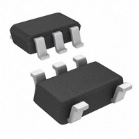
Pin connections (top view)
• Battery-powered applications
• Portable devices
Output
1
VDD
2
Non Inverting Input
3
5
VCC
• Signal conditioning
• Medical instrumentation
4
Inverting Input
SOT23-5
N.C.
1
Inverting Input
2
Non Inverting Input
3
VDD
4
8
N.C.
_
7
VCC
+
6
Output
5
N.C.
SO-8
Features
• Ultra low offset voltage: 25 µV typ, 100 µV max
• Rail-to-rail input/output voltage swing
Description
The TS507 is a high performance rail-to-rail
input/output amplifier with very low offset voltage.
This amplifier uses a new trimming technique that
yields ultra low offset voltages without any need
for external zeroing.
The circuit offers very stable electrical
characteristics over the entire supply voltage
range, and is particularly intended for automotive
and industrial applications.
The TS507 is housed in the space-saving 5-pin
SOT23 package, making it well suited for batterypowered systems. This micropackage simplifies
the PC board design because of its ability to be
placed in small spaces (external dimensions are
2.8 mm x 2.9 mm).
• Operates from 2.7 V to 5.5 V
• High speed: 1.9 MHz
• 45° phase margin with 100 pF
• Low consumption: 0.8 mA at 2.7 V
• Very large signal voltage gain: 131 dB
• High-power supply rejection ratio: 105 dB
• Very high ESD protection 5kV (HBM)
• Latchup immunity
• Available in SOT23-5 micropackage
• Automotive qualification
March 2013
This is information on a product in full production.
DocID10958 Rev 6
1/20
www.st.com
20
�Contents
TS507
Contents
1
Absolute maximum ratings and operating conditions . . . . . . . . . . . . . 3
2
Electrical characteristics . . . . . . . . . . . . . . . . . . . . . . . . . . . . . . . . . . . . . 4
3
Application note . . . . . . . . . . . . . . . . . . . . . . . . . . . . . . . . . . . . . . . . . . . 15
4
3.1
Out-of-the-loop compensation technique . . . . . . . . . . . . . . . . . . . . . . . . . 15
3.2
In-the-loop-compensation technique . . . . . . . . . . . . . . . . . . . . . . . . . . . . 16
Package information . . . . . . . . . . . . . . . . . . . . . . . . . . . . . . . . . . . . . . . . 17
4.1
SOT23-5 package information . . . . . . . . . . . . . . . . . . . . . . . . . . . . . . . . . 17
4.2
SO-8 package . . . . . . . . . . . . . . . . . . . . . . . . . . . . . . . . . . . . . . . . . . . . . 18
5
Ordering information . . . . . . . . . . . . . . . . . . . . . . . . . . . . . . . . . . . . . . . 19
6
Revision history . . . . . . . . . . . . . . . . . . . . . . . . . . . . . . . . . . . . . . . . . . . 19
2/20
DocID10958 Rev 6
�TS507
1
Absolute maximum ratings and operating conditions
Absolute maximum ratings and operating conditions
Table 1. Absolute maximum ratings (AMR)
Symbol
VCC
Vid
Parameter
Value
Supply voltage(1)
Unit
6
Differential input voltage
(2)
Vin
Input voltage
Tstg
Storage temperature
V
±2.5
(3)
VDD-0.3 to VCC+0.3
-65 to +150
°C
(4)(5)
Rthja
Thermal resistance junction to ambient
SOT23-5
SO-8
Rthjc
Thermal resistance junction to case
SOT23-5
SO-8
81
40
Maximum junction temperature
150
°C
5
kV
300
V
2
kV
Tj
HBM: human body model(6)
ESD
MM: machine model
(7)
CDM: charged device
model(8)
Latchup immunity
250
125
°C/W
class A
1. Value with respect to VDD pin.
2. Differential voltages are the non-inverting input terminal with respect to the inverting input terminal.
3. VCC-Vin and Vin must not exceed 6 V.
4. Short-circuits can cause excessive heating and destructive dissipation.
5. Rthja/c are typical values.
6. Human body model: A 100 pF capacitor is charged to the specified voltage, then discharged through a
1.5 kΩ resistor between two pins of the device. This is done for all couples of connected pin combinations
while the other pins are floating.
7. Machine model: A 200 pF capacitor is charged to the specified voltage, then discharged directly between
two pins of the device with no external series resistor (internal resistor < 5 Ω). This is done for all couples of
connected pin combinations while the other pins are floating.
8. Charged device model: all pins and the package are charged together to the specified voltage and then
discharged directly to the ground through only one pin. This is done for all pins.
Table 2. Operating conditions
Symbol
Parameter
VCC
Supply voltage(1)
Vicm
Common mode input voltage range
Vid
Toper
Differential input
Value
Unit
2.7 to 5.5
voltage(2)
Operating free air temperature range
TS507C
TS507I
VDD to VCC
V
±2.5
0 to +85
-40 to +125
°C
1. Value with respect to VDD pin.
2. Differential voltages are the non-inverting input terminal with respect to the inverting input terminal.
DocID10958 Rev 6
3/20
�Electrical characteristics
2
TS507
Electrical characteristics
Table 3. Electrical characteristics at VCC = +5 V, VDD = 0 V, Vicm = VCC/2, Tamb = 25 °C,
RL connected to VCC/2 (unless otherwise specified)(1)
Symbol
Parameter
Conditions
Min.
Typ.
Max.
25
100
250
400
Unit
DC performance
Vio
ΔVio/Δt
Iib
Iio
CMRR
Input offset voltage(2)
Vicm = 0 to 3.8 V, T=25 °C
TS507C full temperature range
TS507I full temperature range
Vicm = 0 V to 5 V, T=25 °C
TS507C full temperature range
TS507I full temperature range
450
550
750
Vio drift vs. temperature
Tmin < Top < Tmax
1
T = 25 °C
TS507C full temperature range
TS507I full temperature range
8
Input bias current
70
75
110
2
Input offset current
T = 25 °C
TS507C full temperature range
TS507I full temperature range
25
35
50
Common mode rejection ratio
20 log (ΔVicm/ΔVio)
Vicm from 0 V to 3.8 V, T=25 °C
TS507C full temperature range
TS507I full temperature range
94
94
91
Vicm from 0 V to 5 V
PSRR
Avd
VOL
4/20
91
90
89
105
Large signal voltage gain
RL = 10 kΩ, Vout= 0.5 V to 4.5 V
Full temperature range
99
98
131
dB
RL = 600Ω, T=25°C
TS507C full temperature range
TS507I full temperature range
67
95
110
120
RL = 10 kΩ, T=25 °C
Full temperature range
4
15
15
RL = 600 Ω, T=25 °C
TS507C full temperature range
TS507I full temperature range
64
90
110
125
RL = 10 kΩ, T=25 °C
Full temperature range
4
15
15
DocID10958 Rev 6
nA
96
Power supply rejection ratio
20 log (ΔVCC/ΔVio)
Low level output voltage
µV/°C
115
VCC from 2.7 V to 5.5 V,
Vicm=Vcc/2, T=25 °C
TS507C full temperature range
TS507I full temperature range
VCC-VOH High level output voltage drop
µV
mV
�TS507
Electrical characteristics
Table 3. Electrical characteristics at VCC = +5 V, VDD = 0 V, Vicm = VCC/2, Tamb = 25 °C,
RL connected to VCC/2 (unless otherwise specified)(1) (continued)
Symbol
Parameter
Conditions
Min.
Typ.
74
60
53
104
Isink
Vout = VCC, Vid=-1 V, T=25 °C
TS507C full temperature range
TS507I full temperature range
Vout = VDD, Vid=1 V, T=25 °C
TS507C full temperature range
TS507I full temperature range
90
77
70
128
Isource
Supply current (per operator)(2)
No load, Vout=VCC/2,
Vicm=0 to 5 V, T=25 °C
Full temperature range
0.85
RL = 2 kΩ, CL = 100 pF,
f = 100 kHz
1.9
MHz
45
Degrees
10
dB
Iout
ICC
Max.
Unit
mA
1.15
1.25
Dynamic performance
GBP
Gain bandwidth product
φm
Phase margin
Gm
Gain margin
SR
Slew rate
RL = 2 kΩ, CL=100 pF,
Vout = 1.25 V to 3.75 V,
10% to 90%
0.6
V/µs
eN
Equivalent input noise voltage
f = 1 kHz
12
nV/√ Hz
iN
Equivalent input noise current
f = 10 kHz
1.2
pA/√Hz
0.0003
%
THD+eN THD + noise
RL = 2 kΩ, CL=100 pF
f=1 kHz, G=1, RL=2 kΩ,
Vicm=2 V, Vout=3.5 Vpp
1. All parameter limits at temperatures different from 25 ° C are guaranteed by correlation.
2. Measurements made at 4 Vicm values: Vicm=0 V, Vicm=3.8 V, Vicm=4.2 V, Vicm=5 V.
DocID10958 Rev 6
5/20
�Electrical characteristics
TS507
Table 4. Electrical characteristics at VCC = +3.3 V, VDD = 0 V, Vicm = VCC/2, Tamb = 25 °C,
RL connected to VCC/2 (unless otherwise specified)(1)
Symbol
Parameter
Conditions
Min.
Typ.
Max.
25
100
250
400
Unit
DC performance
Vio
ΔVio
Iib
Iio
CMRR
Avd
Input offset voltage(2)
6/20
450
550
750
Tmin < Top < Tmax
1
6
Input bias current
T = 25 °C
TS507C full temperature range
TS507I full temperature range
70
75
145
2
Input offset current
T = 25 °C
TS507C full temperature range
TS507I full temperature range
25
40
45
Common mode rejection ratio
20 log (ΔVicm/ΔVio)
Vicm from 0 V to 2.1 V
115
Large signal voltage gain
RL = 10 kΩ, Vout= 0.5 V to 2.8 V
127
RL = 600 Ω, T=25 °C
TS507C full temperature range
TS507I full temperature range
59
85
100
110
RL = 10 kΩ, T=25 °C
Full temperature range
4
15
15
RL = 600 Ω, T=25 °C
TS507C full temperature range
TS507I full temperature range
57
80
100
115
RL = 10 kΩ, T=25 °C
Full temperature range
4
15
15
Low level output voltage
Vout = VCC, Vid=-1 V, T=25 °C
TS507C full temperature range
TS507I full temperature range
33
26
22
48
Vout = VDD, Vid=1 V, T=25 °C
TS507C full temperature range
TS507I full temperature range
37
32
29
56
Isource
Supply current (per
operator)(2)
No load, Vout=VCC/2,
Vicm=0 to 3.3 V, T=25 °C
Full temperature range
DocID10958 Rev 6
µV
µV/°C
nA
dB
Isink
Iout
ICC
Vicm = 0 V to 3.3 V, T=25 °C
TS507C full temperature range
TS507I full temperature range
Vio drift vs. temperature
VCC-VOH High level output voltage drop
VOL
Vicm = 0 to 2.1 V, T=25 °C
TS507C full temperature range
TS507I full temperature range
mV
mA
0.81
1.1
1.2
�TS507
Electrical characteristics
Table 4. Electrical characteristics at VCC = +3.3 V, VDD = 0 V, Vicm = VCC/2, Tamb = 25 °C,
RL connected to VCC/2 (unless otherwise specified)(1) (continued)
Symbol
Parameter
Conditions
Min.
Typ.
Max.
Unit
Dynamic performance
GBP
Gain bandwidth product
RL = 2 kΩ, CL = 100 pF,
f = 100 kHz
1.9
MHz
45
Degrees
10
dB
φm
Phase margin
Gm
Gain margin
SR
Slew rate
RL = 2 kΩ, CL=100 pF,
Vout= 0.5 V to 2.8 V,
10 % to 90 %
0.6
V/µs
eN
Equivalent input noise voltage
f = 1 kHz
12
nV/√ Hz
0.0004
%
THD+eN THD + noise
RL = 2 kΩ, CL=100 pF
f=1 KHz, G=1, RL=2 kΩ,
Vicm=1.15 V, Vout=1.8 Vpp
1. All parameter limits at temperatures different from 25 ° C are guaranteed by correlation.
2. Measurements done at 4 Vicm values: Vicm=0 V, Vicm=2.1 V, Vicm=2.5 V, Vicm=3.3 V.
DocID10958 Rev 6
7/20
�Electrical characteristics
TS507
Table 5. Electrical characteristics at VCC = +2.7 V VDD = 0 V, Vicm = VCC/2, Tamb = 25 °C,
RL connected to VCC/2 (unless otherwise specified)(1)
Symbol
Parameter
Conditions
Min.
Typ.
Max.
25
100
250
400
Unit
DC performance
Vio
ΔVio
Iib
Iio
CMRR
Avd
Input offset voltage(2)
8/20
450
550
750
Tmin < Top < Tmax
1
8
Input bias current
T = 25 °C
TS507C full temperature range
TS507I full temperature range
70
75
160
2
Input offset current
T = 25 °C
TS507C full temperature range
TS507I full temperature range
25
45
45
Common mode rejection ratio
20 log (ΔVicm/ΔVio)
Vicm from 0 V to 1.5 V
115
Large signal voltage gain
RL = 10 kΩ, Vout= 0.5 V to 2.2 V
126
RL = 600 Ω, T=25 °C
TS507C full temperature range
TS507I full temperature range
57
85
100
105
RL = 10 kΩ, T=25 °C
Full temperature range
4
15
15
RL = 600 Ω, T=25 °C
TS507C full temperature range
TS507I full temperature range
57
80
100
115
RL = 10 kΩ, T=25 °C
Full temperature range
4
15
15
Low level output voltage
Vout = VCC, Vid=-1 V, T=25 °C
TS507C full temperature range
TS507I full temperature range
20
15
13
30
Vout = VDD, Vid=1 V, T=25 °C
TS507C full temperature range
TS507I full temperature range
22
19
17
35
Isource
Supply current (per
operator)(2)
No load, Vout=VCC/2,
Vicm=0 to 2.7 V, T=25 °C
Full temperature range
DocID10958 Rev 6
µV
µV/°C
nA
dB
Isink
Iout
ICC
Vicm = 0 V to 2.7 V, T=25 °C
TS507C full temperature range
TS507I full temperature range
Vio drift vs. temperature
VCC-VOH High level output voltage drop
VOL
Vicm = 0 to 1.9 V, T=25 °C
TS507C full temperature range
TS507I full temperature range
mV
mA
0.79
1.1
1.2
�TS507
Electrical characteristics
Table 5. Electrical characteristics at VCC = +2.7 V VDD = 0 V, Vicm = VCC/2, Tamb = 25 °C,
RL connected to VCC/2 (unless otherwise specified)(1) (continued)
Symbol
Parameter
Conditions
Min.
Typ.
Max.
Unit
Dynamic performance
GBP
Gain bandwidth product
RL = 2 kΩ, CL = 100 pF,
f = 100 kHz
1.9
MHz
45
Degrees
11
dB
φm
Phase margin
Gm
Gain margin
SR
Slew rate
RL = 2 kΩ, CL=100 pF,
Vout= 0.5 V to 2.2 V,
10 % to 90 %
0.6
V/µs
eN
Equivalent input noise voltage
f = 1 kHz
12
nV/√Hz
0.0005
%
THD+eN THD + noise
RL = 2 kΩ, CL=100 pF
f=1 KHz, G=1, RL=2 kΩ,
Vicm=0.85 V, Vout=1.2 Vpp
1. All parameter limits at temperatures different from 25 ° C are guaranteed by correlation.
2. Measurements done at 4 Vicm values: Vicm=0 V, Vicm=1.5 V, Vicm=1.9 V, Vicm=2.7 V.
DocID10958 Rev 6
9/20
�Electrical characteristics
TS507
Figure 1. Input offset voltage distribution for
Vicm≤ VCC-1.2 V at T=25 °C
Figure 2. Input offset voltage distribution vs.
temperature for Vicm≤ VCC-1.2 V
30
400
350
300
Vio distribution at T=25°C for 0V