TS616
Dual wide band operational amplifier with high output current
Features
■ ■ ■ ■ ■ ■ ■ ■ ■
Low noise: 2.5nV/√ Hz High output current: 420mA Very low harmonic and intermodulation distortion High slew rate: 420V/µs -3dB bandwidth: 40MHz @ gain = 12dB on 25Ω single-ended load 20.7Vp-p differential output swing on 50Ω load, 12V power supply Current feedback structure 5V to 12V power supply Specified for 20Ω and 50Ω differential load
Output1 1 Inverting Input1 2 Non Inverting Input1 3 8 VCC +
DW SO-8 Exposed-pad (Plastic micropackage)
Pin connections (top view)
+
7 Output2
+
6 Inverting Input2 5 Non Inverting Input2 dice
Applications
■ ■
VCC - 4
Line driver for xDSL Multiple video line driver
Pad Cross Section View Showing Exposed-Pad. This pad must be connected to a (-Vcc) copper area on the PCB
Description
The TS616 is a dual operational amplifier featuring a high output current of 410mA. This driver can be configured differentially for driving signals in telecommunication systems using multiple carriers. The TS616 is ideally suited for xDSL (High Speed Asymmetrical Digital Subscriber Line) applications. This circuit is capable of driving a 10Ω or 25Ω load on a range of power supplies: ±2.5V, 5V, ±6V or +12V. The TS616 is capable of reaching a -3dB bandwidth of 40MHz on 25Ω load with a 12dB gain. This device is designed for high slew rates and demonstrates low harmonic distortion and intermodulation.
April 2007
Rev 4
1/36
www.st.com 36
�Contents
TS616
Contents
1 2 3 4 5 6 Typical application . . . . . . . . . . . . . . . . . . . . . . . . . . . . . . . . . . . . . . . . . . 3 Absolute maximum ratings and operating conditions . . . . . . . . . . . . . 4 Electrical characteristics . . . . . . . . . . . . . . . . . . . . . . . . . . . . . . . . . . . . . 5 Safe operating area . . . . . . . . . . . . . . . . . . . . . . . . . . . . . . . . . . . . . . . . . 16 Intermodulation distortion product . . . . . . . . . . . . . . . . . . . . . . . . . . . . 17 Printed circuit board layout considerations . . . . . . . . . . . . . . . . . . . . . 20
6.1 Thermal information . . . . . . . . . . . . . . . . . . . . . . . . . . . . . . . . . . . . . . . . . 20
7
Noise measurements . . . . . . . . . . . . . . . . . . . . . . . . . . . . . . . . . . . . . . . 23
7.1 7.2 7.3 Measurement of eN . . . . . . . . . . . . . . . . . . . . . . . . . . . . . . . . . . . . . . . . . 24 Measurement of iNn . . . . . . . . . . . . . . . . . . . . . . . . . . . . . . . . . . . . . . . . . 25 Measurement of iNp . . . . . . . . . . . . . . . . . . . . . . . . . . . . . . . . . . . . . . . . . 25
8
Power supply bypassing . . . . . . . . . . . . . . . . . . . . . . . . . . . . . . . . . . . . 26
8.1 8.2 Single power supply . . . . . . . . . . . . . . . . . . . . . . . . . . . . . . . . . . . . . . . . . 26 Channel separation and crosstalk . . . . . . . . . . . . . . . . . . . . . . . . . . . . . . 27
9
Choosing the feedback circuit . . . . . . . . . . . . . . . . . . . . . . . . . . . . . . . . 28
9.1 9.2 The bias of an inverting amplifier . . . . . . . . . . . . . . . . . . . . . . . . . . . . . . . 29 Active filtering . . . . . . . . . . . . . . . . . . . . . . . . . . . . . . . . . . . . . . . . . . . . . . 29
10 11 12 13
Increasing the line level using active impedance matching . . . . . . . . 31 Package information . . . . . . . . . . . . . . . . . . . . . . . . . . . . . . . . . . . . . . . . 34 Ordering information . . . . . . . . . . . . . . . . . . . . . . . . . . . . . . . . . . . . . . . 35 Revision history . . . . . . . . . . . . . . . . . . . . . . . . . . . . . . . . . . . . . . . . . . . 35
2/36
�TS616
Typical application
1
Typical application
Figure 1 shows a schematic of a typical xDSL application using the TS616. Figure 1. Differential line driver for xDSL applications
3 2 8
+ _
+Vcc 1
12.5 Ω
1/2 TS615 TS616
Vi
R2
R1 GND R4
Vo 25Ω Vo
12.5 Ω
1:2
100Ω
Vi
4 5
_
R3
1/2 TS615 TS616
+
4
-Vcc
3/36
�Absolute maximum ratings and operating conditions
TS616
2
Absolute maximum ratings and operating conditions
Table 1.
Symbol VCC Vid Vin Toper Tstd Tj Rthjc Rthja Pmax ESD only pins 1, 4, 7, 8 ESD only pins 2, 3, 5, 6 Supply voltage (1) Differential input voltage Input voltage range
(3) (2)
Absolute maximum ratings
Parameter Value ±7 ±2 ±6 -40 to + 85 -65 to +150 150 16 60 2 1.5 2 200 1.5 2 100
(4)
Unit V V V °C °C °C °C/W °C/W W kV kV V kV kV V
Operating free air temperature range Storage temperature Maximum junction temperature Thermal resistance junction to case Thermal resistance junction to ambient area Maximum power dissipation (@Tamb = 25°C) for Tj = 150°C CDM: charged device model HBM: human body model MM: machine model CDM: charged device model HBM: human body model MM: machine model Output short circuit
1. All voltage values, except differential voltage are with respect to network terminal. 2. Differential voltages are non-inverting input terminal with respect to the inverting input terminal. 3. The magnitude of input and output voltage must never exceed VCC +0.3V. 4. An output current limitation protects the circuit from transient currents. Short-circuits can cause excessive heating. Destructive dissipation can result from short-circuits on amplifiers.
Table 2.
Symbol VCC Vicm
Operating conditions
Parameter Power supply voltage Common mode input voltage Value ±2.5 to ±6 -VCC+1.5V to +VCC-1.5V Unit V V
4/36
�TS616
Electrical characteristics
3
Table 3.
Symbol
Electrical characteristics
VCC = ±6V, Rfb= 910Ω Tamb = 25°C (unless otherwise specified) ,
Parameter Test conditions Min. Typ. Max. Unit
DC performance Vio ΔVio Iib+ Input offset voltage Differential input offset voltage Positive input bias current Tamb Tmin < Tamb < Tmax Tamb = 25°C Tamb Tmin < Tamb < Tmax Negative input bias current Input(+) impedance Input(-) impedance Input(+) capacitance Common mode rejection ratio 20 log (ΔVic/ΔVio) Supply voltage rejection ratio 20 log (ΔVCC/ΔVio) Total supply current per operator ΔVic = ±4.5V Tmin < Tamb < Tmax ΔVCC = ±2.5V to ±6V Tmin < Tamb < Tmax No load 72 58 Tamb Tmin < Tamb < Tmax 5 7.2 3 3.1 82 54 1 64 dB 62 81 dB 80 13.5 17 mA kΩ Ω pF 15 µA 1 1.6 2.5 30 µA mV 3.5 mV
IibZIN+ ZINCIN+ CMR
SVR ICC
Dynamic performance and output characteristics ROL Open loop transimpedance Vout = 7Vp-p, RL = 25Ω Tmin < Tamb < Tmax -3dB bandwidth BW Full power bandwidth Gain flatness @ 0.1dB Tr Tf Ts SR VOH VOL Rise time Fall time Settling time Slew rate High level output voltage Low level output voltage Small signal Vout < 20mVp AV = 12dB, RL = 25Ω Large signal Vout = 3Vp AV = 12dB, RL = 25Ω Small signal Tamb
很抱歉,暂时无法提供与“TS616IDW”相匹配的价格&库存,您可以联系我们找货
免费人工找货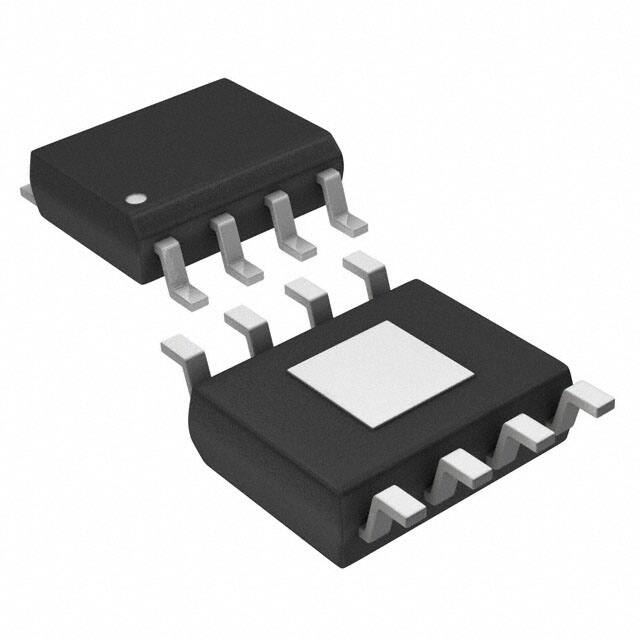


 工商网监
湘ICP备2023018690号
工商网监
湘ICP备2023018690号
