TS925
Rail-to-rail high output current quad operational amplifiers
with standby mode and adjustable phantom ground
Features
■
Rail-to-rail input and output
■
Low noise: 9 nV/√Hz
■
Low distortion
■
High output current: 80 mA (able to drive 32 Ω
loads)
■
High-speed: 4 MHz, 1.3 V/μs
■
Operating range from 2.7 to 12 V
■
Low input offset voltage: 900 μV max.
(TS925A)
■
Adjustable phantom ground (VCC/2)
■
Standby mode
■
ESD internal protection: 2 kV
■
Latch-up immunity
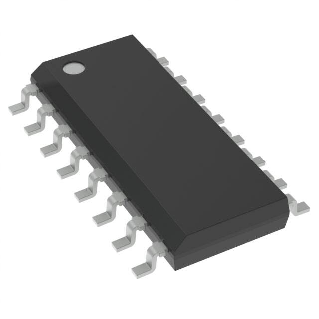
D
SO-16
(Plastic micropackage)
P
TSSOP16
(Thin shrink small outline package)
Pin connections (top view)
Applications
■
MPEG boards, multimedia systems
■
Cordless telephones and portable
communication equipment
■
■
+
+
16
Output 4
15
Inverting
Input 4
-
Non-inverting
Input 1
3
14
Non-inverting
Input 4
V CC+
4
13
V CC -
Non-inverting
Input 2
5
12
Non-inverting
Input 3
Inverting
Input 2
6
11
Inverting
Input 3
Output 2
7
10
Output 3
Phantom ground
8
9
Line drivers, buffers
Instrumentation with low noise as key factor
-
-
Soundcard amplifiers, piezoelectric speakers
2
+
■
Inverting
Input 1
+
Headphone amplifiers
1
-
■
Output 1
Stdby
Description
The TS925 is a rail-to-rail quad BiCMOS
operational amplifier optimized and fully specified
for 3- and 5-V operation.
The TS925 exhibits very low noise, low distortion
and high output current, making this device an
excellent choice for high-quality, low-voltage or
battery-operated audio/telecom systems.
High output current allows low load impedances
to be driven. An internal low impedance phantom
ground eliminates the need for an external
reference voltage or biasing arrangement.
The device is stable for capacitive loads up to
500 pF. When the STANDBY mode is enabled, the
total consumption drops to 6 μA (VCC = 3 V).
April 2011
Doc ID 4949 Rev 4
1/18
www.st.com
18
�Absolute maximum ratings and operating conditions
1
TS925
Absolute maximum ratings and operating conditions
Table 1.
Symbol
Absolute maximum ratings
Value
Unit
Supply voltage (1)
14
V
Vid
Differential input voltage (2)
±1
V
Vi
Input voltage
VDD -0.3 to VCC +0.3
V
Tj
Maximum junction temperature
150
°C
Rthja
Thermal resistance junction to
ambient
SO-16
TSSOP16
95
95
°C/W
Rthjc
Thermal resistance junction to
case
SO-16
TSSOP16
30
25
°C/W
HBM
Human body model(3)
2
kV
200
V
1
kV
VCC
ESD
Parameter
Conditions
Electrostatic discharge
MM
Machine model(4)
CDM
Charged device model
See note(5)
Output short circuit duration
Latch-up immunity
Soldering temperature
10 sec,
Pb-free package
200
mA
260
°C
1. All voltage values, except differential voltage are with respect to network ground terminal.
2. Differential voltages are the non-inverting input terminal with respect to the inverting input terminal. If
Vid > ±1 V, the maximum input current must not exceed ±1mA. In this case (Vid > ±1V), an input series
resistor must be added to limit input current.
3. Human body model: 100pF discharged through a 1.5 kΩ resistor into pin of device.
4. Machine model ESD: a 200 pF cap is charged to the specified voltage, then discharged directly into the IC
with no external series resistor (internal resistor < 5 Ω), into pin-to-pin of device.
5. There is no short-circuit protection inside the device: short-circuits from the output to Vcc can cause
excessive heating. The maximum output current is approximately 80 mA, independent of the magnitude of
Vcc. Destructive dissipation can result from simultaneous short-circuits on all amplifiers.
Table 2.
Operating conditions
Symbol
2/18
Parameter
VCC
Supply voltage
Vicm
Common mode input voltage range
Toper
Operating free air temperature range
Doc ID 4949 Rev 4
Value
Unit
2.7 to 12
V
VDD -0.2 to VCC +0.2
V
-40 to +125
°C
�TS925
2
Electrical characteristics
Electrical characteristics
Table 3.
Electrical characteristics for VCC = 3 V with VDD = 0 V, Vicm = VCC/2,
RL connected to VCC/2, Tamb = 25° C
(unless otherwise specified)
Symbol
Parameter
Conditions
Min.
Typ.
Max.
Unit
DC performance
Vio
DVio
At Tamb = +25°C
TS925
TS925A
At Tmin. ≤Tamb ≤Tmax:
TS925
TS925A
Input offset voltage
mV
3
0.9
5
1.8
Input offset voltage drift
μV/°C
2
Iio
Input offset current
Vout = 1.5V
1
30
nA
Iib
Input bias current
Vout = 2.5V
15
100
nA
CMR
Common mode rejection
ratio
Vicm from 0 to 3 V
Tmin ≤ Tamb ≤ Tmax
60
VOH
High level output voltage
RL = 10kΩ
RL = 600Ω
RL = 32Ω
2.90
2.87
VOL
Low level output voltage
80
dB
V
2.63
RL = 10kΩ
RL = 600Ω
RL = 32Ω
180
Vout = 2Vpk-pk
RL = 10kΩ
RL = 600Ω
RL = 32Ω
200
35
16
50
100
mV
V/mV
Avd
Large signal voltage gain
SVR
Supply voltage rejection ratio Vcc = 2.7 to 3.3V
60
85
dB
Output short-circuit current
50
80
mA
Io
ICC
Total supply current
No load, Vout = Vcc/2
5
Istby
Total supply current in
STANDBY
Pin 9 connected to Vcc-
6
Venstby
Pin 9 voltage to enable the
STANDBY mode (1)
at Tamb = +25°C
at Tmin ≤Tamb ≤Tmax
Vdistby
Pin 9 voltage to disable the
STANDBY mode(1)
at Tamb = +25°C
at Tmin ≤Tamb ≤Tmax
7
mA
μA
0.3
0.4
V
1.1
1
V
AC performance
GBP
Gain bandwidth product
SR
Slew rate
Pm
Phase margin at unit gain
RL = 600Ω
0.7
RL = 600Ω, CL =100pF
Doc ID 4949 Rev 4
4
MHz
1.3
V/μs
68
Degrees
3/18
�Electrical characteristics
Table 3.
TS925
Electrical characteristics for VCC = 3 V with VDD = 0 V, Vicm = VCC/2,
RL connected to VCC/2, Tamb = 25° C
(unless otherwise specified) (continued)
Symbol
Parameter
Conditions
GM
Gain margin
RL = 600Ω, CL =100pF
en
Equivalent input noise
voltage
f = 1kHz
Total harmonic distortion
Vout = 2Vpk-pk,
f = 1kHz, Av = 1,
RL = 600Ω
THD
Cs
Min.
Channel separation
Typ.
Max.
Unit
12
dB
9
nV
-----------Hz
0.01
%
120
dB
Phantom ground
Vpg
Phantom ground output
voltage
Ipgsc
Phantom ground output short
circuit current - sourced
Zpg
Phantom ground impedance
DC to 20kHz
Enpg
Phantom ground output
voltage noise
f = 1kHz
Cdec = 100pF
Cdec = 1nF
Cdec = 10nF(2)
Ipgsk
Phantom ground output short
circuit current - sinked
No output current
Vcc/2
-5%
Vcc/2
12
18
mA
3
Ω
200
40
17
nV
-----------Hz
18
mA
12
Vcc/2
+5%
1. The STANDBY mode is enabled when pin 9 is GROUNDED and disabled when pin 9 is left OPEN.
2. Cdec is the decoupling capacitor on pin 9.
4/18
Doc ID 4949 Rev 4
V
�TS925
Electrical characteristics
Table 4.
Electrical characteristics for VCC = 5 V, VDD = 0 V, Vicm = VCC/2,
RL connected to VCC/2, Tamb = 25° C
(unless otherwise specified)
Symbol
Parameter
Conditions
Min.
Typ.
Max.
Unit
DC performance
Vio
DVio
At Tamb = +25°C:
TS925
TS925A
At Tmin. ≤Tamb ≤Tmax:
TS925
TS925A
Input offset voltage
3
0.9
mV
5
1.8
Input offset voltage drift
μV/°C
2
Iio
Input offset current
Vout = 2.5V
1
30
nA
Iib
Input bias current
Vout = 2.5V
15
100
nA
CMR
Common mode rejection
ratio
Vicm from 0 to 5 V
Tmin ≤ Tamb ≤ Tmax
VOH
High level output voltage
RL= 10kΩ
RL = 600Ω
RL = 32Ω
VOL
Low level output voltage
60
80
dB
4.90
4.85
V
4.4
50
120
RL= 10kΩ
RL = 600Ω
RL = 32Ω
300
Vout = 2Vpk-pk
RL= 10k
RL = 600Ω
RL = 32Ω
200
40
17
V/mV
mV
Avd
Large signal voltage gain
SVR
Supply voltage rejection ratio Vcc = 3 to 5V
60
85
dB
Output short-circuit current
50
80
mA
Io
ICC
Total supply current
No load, Vout = Vcc/2
6
Istby
Total supply current in
STANDBY
Pin 9 connected to Vcc-
6
Venstby
Pin 9 Voltage to enable the
STANDBY mode (1)
at Tamb = +25°C
at Tmin ≤Tamb ≤Tmax
Vdistby
Pin 9 voltage to disable the
STANDBY mode (1)
at Tamb = +25°C
at Tmin ≤Tamb ≤Tmax
8
μA
0.3
0.4
1.1
1
mA
V
V
AC performance
GBP
Gain bandwidth product
RL = 600Ω
0.7
4
MHz
1.3
V/μs
SR
Slew rate
Pm
Phase margin at unit gain
RL = 600Ω, CL =100pF
68
Degrees
GM
Gain margin
RL = 600Ω, CL =100pF
12
dB
Doc ID 4949 Rev 4
5/18
�Electrical characteristics
Table 4.
Electrical characteristics for VCC = 5 V, VDD = 0 V, Vicm = VCC/2,
RL connected to VCC/2, Tamb = 25° C
(unless otherwise specified) (continued)
Symbol
en
THD
Cs
TS925
Parameter
Conditions
Equivalent input noise
voltage
f = 1kHz
Total harmonic distortion
Vout = 2Vpk-pk,
f = 1kHz, Av = 1,
RL = 600Ω
Min.
Channel separation
Typ.
Max.
Unit
9
nV
-----------Hz
0.01
%
120
dB
Phantom ground
Vpg
Phantom ground output
voltage
Ipgsc
Phantom ground output
short circuit current sourced
Zpg
Phantom ground impedance DC to 20kHz
Enpg
Phantom ground output
voltage noise
Ipgsk
Phantom ground output
short circuit current - sinked
No output current
Vcc/2
-5%
Vcc/2
12
18
mA
3
Ω
200
40
17
nV
-----------Hz
18
mA
f = 1kHz
Cdec = 100pF
Cdec = 1nF
Cdec = 10nF(2)
12
Vcc/2
+5%
1. The STANDBY mode is enabled when pin 9 is GROUNDED and disabled when pin 9 is left OPEN.
2. Cdec is the decoupling capacitor on pin 9.
6/18
Doc ID 4949 Rev 4
V
�TS925
Electrical characteristics
Figure 1.
Input offset voltage distribution
Figure 2.
Total supply current vs. supply
voltage with no load
Figure 3.
Supply current/amplifier vs.
temperature
Figure 4.
Output short circuit current vs.
output voltage
Figure 5.
Output short circuit current vs.
output voltage
Figure 6.
Output short circuit current vs.
output voltage
Doc ID 4949 Rev 4
7/18
�Electrical characteristics
TS925
Figure 7.
Output short circuit current vs.
temperature
Figure 8.
Figure 9.
Distortion + noise vs. frequency
Figure 10. THD + noise vs. frequency
Figure 11. THD + noise vs. frequency
8/18
Voltage gain and phase vs.
frequency
Figure 12. THD + noise vs. frequency
Doc ID 4949 Rev 4
�TS925
Electrical characteristics
Figure 13. Equivalent input noise vs.
frequency
Figure 14. Total supply current vs. standby
input voltage
Figure 15. Phantom ground short circuit
output current vs. phantom ground
output voltage
Doc ID 4949 Rev 4
9/18
�Using the TS925 as a preamplifier and speaker driver
3
TS925
Using the TS925 as a preamplifier and speaker driver
The TS925 is an input/output rail-to-rail quad BiCMOS operational amplifier. It can operate
with low supply voltages (2.7 V) and drive output loads as low as 32 Ω.
This section illustrates these features by providing an example of how the device can be
used as a preamplifier and speaker driver.
The application circuit is shown in Figure 16.
●
Operators A1and A4 are used in a preamplifier configuration.
●
Operators A2 and A3 are used in a push-pull configuration driving a headset.
●
The phantom ground is used as a common reference level (VCC/2).
●
The power supply is delivered by two LR6 batteries (2 x 1.5 V nominal).
Figure 16. Electrical schematic
M ike pream plifier
C1
C9
M IK E
OUTPUT
R2
M IC R O P H O N E
R5
C6
R3
C4
C 14
D2
D1
C5
C2
C3
C7
R7
R17
R18
A LC
Q1
R8
V cc
P H A N TO M G R O U N D
8
4
13
9
STBY
C15
C10
C18 C8
7
5
HEADPHONES
R 12
R13
6
C 10
H eadphones am plifier
R15
C 12
R 11
R10
C9
C 13
A M P LIF IE R
IN P U T
LE F T
11
10
10/18
Doc ID 4949 Rev 4
R16
C 11
12
A M P LIF IE R
IN P U T
R IG H T
�TS925
3.1
Using the TS925 as a preamplifier and speaker driver
Preamplifier configuration
The operators A1 and A4 are wired with a non-inverting gain of respectively:
●
A1# (R4/(R3+R17))
●
A4# R6/R5
With the following values:
●
R4 = 22 kΩ - R3 = 50 Ω - R17 = 1.2 kΩ
●
R6 = 47 kΩ - R5 = 1.2 kΩ,
The gain of the preamplifier chain is therefore equal to 58 dB.
Alternatively, the gain of A1 can be adjusted by choosing a JFET transistor Q1 instead of
R17. This JFET voltage controlled resistor arrangement forms an automatic level control
(ALC) circuit, useful in many microphone preamplifier applications. The mean rectified peak
level of the output signal envelope is used to control the preamplifier gain.
3.2
Headphone amplifier
The operators A2 and A3 are organized in a push-pull configuration with a gain of 5. The
stereo inputs can be connected to a CD player and the TS925 can directly drive the headphone speakers. This configuration shows the ability of the circuit to drive a 32 Ω load with a
maximum output swing and high fidelity suitable for sound and music.
Figure 19 shows the available signal swing at the headset outputs: two other rail-to-rail
competitor parts are employed in the same circuit for comparison (note the much-reduced
clipping level and crossover distortion).
Doc ID 4949 Rev 4
11/18
�Using the TS925 as a preamplifier and speaker driver
Figure 17. Frequency response of the global
preamplifier chain
TS925
Figure 18. Voltage noise density vs. frequency
at preamplifier output
15
70
14
Nois e D e n s it y ( nV / s qrt(Hz ) )
V o ltag e Gain (d B)
60
50
40
30
13
12
11
10
9
8
20
100
100 0
10 000
10 00 00
1 00 000 0
1 00 000 00
1.0E + 0 8
7
10
frequency (Hz)
100
10 0 0
1 0 000
10 0 00 0
fre q u e ncy (H z)
Figure 19. Maximum voltage swing at
headphone outputs (RL = 32 Ω)
Figure 20. THD + noise vs. frequency
(headphone outputs)
0.4
0 .3 5
THD+no ise (%)
0.3
0 .2 5
0.2
0 .1 5
0.1
0 .0 5
0
1 00
1 000
10 000
Hz
12/18
Doc ID 4949 Rev 4
10 0000
�TS925
4
Package information
Package information
In order to meet environmental requirements, ST offers these devices in different grades of
ECOPACK® packages, depending on their level of environmental compliance. ECOPACK®
specifications, grade definitions and product status are available at: www.st.com.
ECOPACK® is an ST trademark.
Doc ID 4949 Rev 4
13/18
�Package information
4.1
TS925
SO-16 package information
Figure 21. SO-16 package mechanical drawing
Table 5.
SO-16 package mechanical data
Dimensions
Millimeters
Inches
Ref.
Min.
Typ.
A
Max.
Min.
Typ.
1.75
0.069
A1
0.10
A2
1.25
b
0.31
0.51
0.012
0.020
c
0.17
0.25
0.007
0.010
D(1)
9.80
9.90
10.00
0.386
0.390
0.394
E
5.80
6.00
6.20
0.228
0.236
0.244
E1(2)
3.80
3.90
4.00
0.150
0.154
0.157
e
0.25
Max.
0.004
0.010
0.049
1.27
0.050
h
0.25
0.50
0.010
0.020
L
0.40
1.27
0.016
0.050
k
0
8
ccc
0.10
0.004
1. Does not include mold flash, protrusions or gate burrs. Mold flash, protrusions or gate burrs not to exceed
0.15 mm in total.
2. Does not include interlead flash or protrusions. Interlead flash or protrusions not to exceed 0.25 mm per
side.
14/18
Doc ID 4949 Rev 4
�TS925
4.2
Package information
TSSOP16 package information
Figure 22. TSSOP16 package mechanical drawing
b
Table 6.
TSSOP16 package mechanical data
Dimensions
Ref.
Millimeters
Min.
Typ.
A
Inches
Max.
Min.
Typ.
1.20
A1
0.05
A2
0.80
b
Max.
0.047
0.15
0.002
1.05
0.031
0.19
0.30
0.007
0.012
c
0.09
0.20
0.004
0.008
D
4.90
5.00
5.10
0.193
0.197
0.201
E
6.20
6.40
6.60
0.244
0.252
0.260
E1
4.30
4.40
4.50
0.169
0.173
0.177
e
0.65
k
0°
L
0.45
L1
aaa
1.00
0.60
0.006
0.039
0.041
0.0256
8°
0°
0.75
0.018
1.00
8°
0.024
0.030
0.039
0.10
Doc ID 4949 Rev 4
0.004
15/18
�Ordering information
5
TS925
Ordering information
Order code
Temperature range
TS925ID/IDT
TS925IPT
TS925AID/AIDT
TS925AIPT
16/18
-40°C to +125°C
Package
Packing
SO-16
Tube and tape & reel
TSSOP16
Tape & reel
SO-16
Tube and tape & reel
TSSOP16
Tape & reel
Doc ID 4949 Rev 4
Marking
925I
925AI
�TS925
6
Revision history
Revision history
01-
Table 7.
Document revision history
Date
Revision
01-Feb-2001
1
Initial release. Product in full production.
2
The following changes were made in this revision:
– Chapter on Macromodels removed from the datasheet.
– Data updated in Table 3. on page 3.
– Data in tables in Electrical characteristics on page 3 reformatted
for easier use.
– Minor grammatical and formatting changes throughout.
10-Mar-2009
3
Document reformatted.
Removed DIP package information in Chapter 4 and associated
order codes in Chapter 5.
Updated SO-16 and TSSOP16 package drawings and dimensions in
Chapter 4.
28-Apr-2011
4
Modified CMR conditions in Table 3 and Table 4.
01-Nov-2005
Changes
Doc ID 4949 Rev 4
17/18
�TS925
Please Read Carefully:
Information in this document is provided solely in connection with ST products. STMicroelectronics NV and its subsidiaries (“ST”) reserve the
right to make changes, corrections, modifications or improvements, to this document, and the products and services described herein at any
time, without notice.
All ST products are sold pursuant to ST’s terms and conditions of sale.
Purchasers are solely responsible for the choice, selection and use of the ST products and services described herein, and ST assumes no
liability whatsoever relating to the choice, selection or use of the ST products and services described herein.
No license, express or implied, by estoppel or otherwise, to any intellectual property rights is granted under this document. If any part of this
document refers to any third party products or services it shall not be deemed a license grant by ST for the use of such third party products
or services, or any intellectual property contained therein or considered as a warranty covering the use in any manner whatsoever of such
third party products or services or any intellectual property contained therein.
UNLESS OTHERWISE SET FORTH IN ST’S TERMS AND CONDITIONS OF SALE ST DISCLAIMS ANY EXPRESS OR IMPLIED
WARRANTY WITH RESPECT TO THE USE AND/OR SALE OF ST PRODUCTS INCLUDING WITHOUT LIMITATION IMPLIED
WARRANTIES OF MERCHANTABILITY, FITNESS FOR A PARTICULAR PURPOSE (AND THEIR EQUIVALENTS UNDER THE LAWS
OF ANY JURISDICTION), OR INFRINGEMENT OF ANY PATENT, COPYRIGHT OR OTHER INTELLECTUAL PROPERTY RIGHT.
UNLESS EXPRESSLY APPROVED IN WRITING BY AN AUTHORIZED ST REPRESENTATIVE, ST PRODUCTS ARE NOT
RECOMMENDED, AUTHORIZED OR WARRANTED FOR USE IN MILITARY, AIR CRAFT, SPACE, LIFE SAVING, OR LIFE SUSTAINING
APPLICATIONS, NOR IN PRODUCTS OR SYSTEMS WHERE FAILURE OR MALFUNCTION MAY RESULT IN PERSONAL INJURY,
DEATH, OR SEVERE PROPERTY OR ENVIRONMENTAL DAMAGE. ST PRODUCTS WHICH ARE NOT SPECIFIED AS "AUTOMOTIVE
GRADE" MAY ONLY BE USED IN AUTOMOTIVE APPLICATIONS AT USER’S OWN RISK.
Resale of ST products with provisions different from the statements and/or technical features set forth in this document shall immediately void
any warranty granted by ST for the ST product or service described herein and shall not create or extend in any manner whatsoever, any
liability of ST.
ST and the ST logo are trademarks or registered trademarks of ST in various countries.
Information in this document supersedes and replaces all information previously supplied.
The ST logo is a registered trademark of STMicroelectronics. All other names are the property of their respective owners.
© 2011 STMicroelectronics - All rights reserved
STMicroelectronics group of companies
Australia - Belgium - Brazil - Canada - China - Czech Republic - Finland - France - Germany - Hong Kong - India - Israel - Italy - Japan Malaysia - Malta - Morocco - Philippines - Singapore - Spain - Sweden - Switzerland - United Kingdom - United States of America
www.st.com
18/18
Doc ID 4949 Rev 4
�