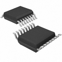
TS925
RAIL TO RAIL HIGH OUTPUT CURRENT
QUAD OPERATIONAL AMPLIFIER
■
■
■
■
■
■
■
■
RAIL TO RAIL INPUT AND OUTPUT
LOW NOISE : 9nV/√Hz
LOW DISTORTION
HIGH OUTPUT CURRENT : 80mA
(able to drive 32Ω loads)
HIGH SPEED : 4MHz, 1.3V/µs
OPERATING FROM 2.7V TO 12V
LOW INPUT OFFSET VOLTAGE : 900µV
max. (TS925A)
N
DIP16
(Plastic Package)
■ ADJUSTABLE PHANTOM GROUND (VCC/2)
■ STANDBY MODE
■
■
■
■
D
SO16
(Plastic Micropackage)
ESD INTERNAL PROTECTION : 2kV
LATCH-UP IMMUNITY
MACROMODEL INCLUDED IN THIS
SPECIFICATION
DESCRIPTION
P
TSSOP16
(Thin Shrink Small Outline Package)
The TS925 is a RAIL TO RAIL quad BiCMOS operational amplifier optimized and fully specified for
3V and 5V operation.
APPLICATIONS
■
■
■
■
Headphone amplifier
Soundcard amplifier, piezoelectric speaker
MPEG boards, multimedia systems, ...
Cordless telephones and portable communication equipment
■ Line driver, buffer
■ Instrumentation with low noise as key factor
February 2001
-40°C, +125°C
N
D
P
•
•
•
N = Dual in Line Package (DIP)
D = Small Outline Package (SO) - also available in Tape & Reel (DT)
P = Thin Shrink Small Outline Package (TSSOP) - only available
in Tape & Reel (PT)
PIN CONNECTIONS (top view)
Output 1
1
16
Output 4
Inverting
Input 1
2
15
Inverting
Input 4
3
14
Non-inverting
Input 4
4
13
V CC -
12
Non-inverting
Input 3
11
Inverting
Input 3
Output 3
Non-inverting
Input 1
V CC+
-
+
+
-
Non-inverting
Input 2
5
Inverting
Input 2
6
Output 2
7
10
Phantom ground
8
9
-
When the STANDBY mode is enabled, the total
consumption drops to 6µA (VCC = 3V).
TS925I
Package
Temperature
Range
+
The device is stable for capacitive loads up to
500pF.
Part Number
+
The TS925 exhibits a very low noise, low distortion and high output current making this device an
excellent choice for high quality, low voltage or
battery operated audio/telecom systems.
ORDER CODE
-
High output current allows low load impedances to
be driven. An internal low impedance PHANTOM
GROUND eliminates the need for an external reference voltage or biasing arrangement.
Stdby
1/15
�TS925
ABSOLUTE MAXIMUM RATINGS
Symbol
Parameter
Unit
VCC
Supply voltage 1)
14
V
Vid
Differential Input Voltage 2)
±1
V
Vi
Toper
Tj
Rthja
Input Voltage
3)
Operating Free Air Temperature Range
Maximum Junction Temperature
Thermal Resistance Junction to Ambient
Output Short Circuit Duration
1.
2.
3.
4.
Value
-0.3 to 14
V
-40 to +125
°C
150
°C
130
see note 4)
°C/W
°C
All voltage values, except differential voltage are with respect to network ground terminal.
Differential voltages are the non-inverting input terminal with respect to the inverting input t erminal.
The magnitude of input and output voltages must never exceed VCC + +0.3V.
Short-circuits can cause excessive heating. Destructive dissipation can result from simultaneous short-circuit on all amplifiers.
Do not short circuit outputs to VCC+ when exceeding 8V : this can induce reliability defects.
OPERATING CONDITIONS
Symbol
VCC
Vicm
2/15
Parameter
Value
Supply voltage
Common Mode Input Voltage Range
Unit
2.7 to 12
-
V
+
VCC -0.2 to VCC +0.2
V
�TS925
ELECTRICAL CHARACTERISTICS
VCC+ = 3V, VCC- = 0V, Tamb = 25°C (unless otherwise specified)
OPERATIONAL AMPLIFIER
Symbol
Parameter
Input Offset Voltage
Vio
DVio
Tmin. ≤ Tamb ≤ Tmax.
Min.
Typ.
TS925
TS925A
TS925
TS925A
Max.
Unit
3
0.9
5
1.8
mV
µV/°C
Input Offset Voltage Drift
2
Iio
Input Offset Current
Vout = 1.5V
1
30
Iib
Input Bias Current
Vout = 1.5V
15
100
VOH
VOL
Avd
High Level Output Voltage
RL connected to Vcc/2
Low Level Output Voltage
RL connected to Vcc/2
nA
nA
RL= 10k
RL = 600Ω
RL = 32Ω
2.90
2.87
V
2.63
RL= 10k
RL = 600Ω
RL = 32Ω
180
Large Signal Voltage Gain (Vout = 2Vpk-pk) RL= 10k
RL = 600Ω
RL = 32Ω
200
35
16
50
100
GBP
Gain Bandwith Product
RL = 600Ω
CMR
Common Mode Rejection Ratio
60
80
SVR
Supply Voltage Rejection Ratio
Vcc = 2.7 to 3.3V
60
85
Output Short-Circuit Current
50
80
SR
Slew Rate
0.7
1.3
Pm
Phase Margin at Unit Gain
RL = 600Ω, CL =100pF
68
GM
Gain Margin
RL = 600Ω, CL =100pF
12
Equivalent Input Noise Voltage
f = 1kHz
9
Io
en
THD
Cs
mV
V/mV
MHz
4
dB
dB
mA
V/µs
Degrees
dB
Total Harmonic Distortion
Vout = 2Vpk-pk, F = 1kHz, Av = 1, RL =600Ω
0.01
Channel Separation
120
nV
-----------Hz
%
dB
3/15
�TS925
GLOBAL CIRCUIT
Symbol
Parameter
ICC
Total Supply Current
No load, Vout = Vcc/2
Istby
Total Supply Current in STANDBY
(pin 9 connected to Vcc-)
Venstby
Pin 9 Voltage to enable the STANDBY mode 1)
Tmin ≤ Tamb ≤ Tmax
Vdistby
Pin 9 Voltage to disable the STANDBY mode (see note1)
Tmin ≤ Tamb ≤ Tmax
1.
Min.
Typ
Max.
5
7
Unit
mA
µA
6
0.3
0.4
1.1
1
V
V
the STANDBY mode is currently enabled when Pin 9 is GROUNDED and disabled when Pin 9 is left OPEN.
PHANTOM GROUND
Symbol
Parameter
Vpg
Phantom Ground Output Voltage
No Output Current
Ipgsc
Phantom Ground Output Short Circuit Current (sourced)
Zpg
Phantom Ground Impedance
DC to 20kHz
Enpg
Phantom Ground Output Voltage Noise (f=1kHz)
Cdec = 100pF
Cdec = 1nF
Min.
Typ
Max.
Unit
Vcc/2
-5%
Vcc/2
Vcc/2
+5%
V
12
18
Ω
3
Cdec = 10nF1)
Ipgsk
1.
4/15
Phantom Ground Output Short Circuit Current (sinked)
Cdec is the decoupling capacitor on Pin9
mA
12
200
40
17
nV
-----------Hz
18
mA
�TS925
ELECTRICAL CHARACTERISTICS
VCC+ = 5V, VCC- = 0V, Tamb = 25°C (unless otherwise specified)
Symbol
Parameter
Input Offset Voltage
Vio
DVio
Tmin. ≤ Tamb ≤ Tmax.
Min.
Typ.
TS925
TS925A
TS925
TS925A
Max.
Unit
3
0.9
5
1.8
mV
µV/°C
Input Offset Voltage Drift
2
Iio
Input Offset Current
Vout = 2.5V
1
30
Iib
Input Bias Current
Vout = 2.5V
15
100
VOH
VOL
Avd
High Level Output Voltage
RL connected to Vcc/2
Low Level Output Voltage
RL connected to Vcc/2
Large Signal Voltage Gain
Vout = 4Vpk-pk
Vout = 4Vpk-pk
nA
nA
RL= 10k
RL = 600Ω
RL = 32Ω
4.90
4.85
V
4.4
RL= 10k
RL = 600Ω
RL = 32Ω
300
RL = 10k
RL= 600Ω
RL= 32Ω
200
40
17
50
120
GBP
Gain Bandwith Product
RL = 600Ω
CMR
Common Mode Rejection Ratio
60
80
SVR
Supply Voltage Rejection Ratio
Vcc = 3V to 5V
60
85
Io
mV
V/mV
MHz
4
dB
dB
Output Short-Circuit Current
50
80
mA
SR
Slew Rate
0.7
1.3
V/µs
Pm
Phase Margin at Unit Gain
RL = 600Ω, CL =100pF
68
GM
Gain Margin
RL = 600Ω, CL =100pF
12
Equivalent Input Noise Voltage
f = 1kHz
9
en
THD
Cs
Degrees
dB
Total Harmonic Distortion
Vout = 3Vpk-pk, F = 1kHz, Av = 1, RL =600Ω
0.01
Channel Separation
120
nV
-----------Hz
%
dB
5/15
�TS925
GLOBAL CIRCUIT
Symbol
Parameter
ICC
Total Supply Current
No load, Vout = Vcc/2
Istby
Total Supply Current in STANDBY
(pin 9 connected to Vcc-)
Venstby
Pin 9 Voltage to enable the STANDBY mode 1)
Tmin ≤ Tamb ≤ Tmax
Vdistby
Pin 9 Voltage to disable the STANDBY mode (see note1)
Tmin ≤ Tamb ≤ Tmax
1.
Min.
Typ
6
Max.
8
Unit
mA
µA
10
0.3
0.4
1.1
1
V
V
the STANDBY mode is currently enabled when Pin 9 is GROUNDED and disabled when Pin 9 is left OPEN.
PHANTOM GROUND
Symbol
Parameter
Vpg
Phantom Ground Output Voltage
No Output Current
Ipgsc
Phantom Ground Output Short Circuit Current (sourced)
Zpg
Phantom Ground Impedance
DC to 20kHz
Enpg
Phantom Ground Output Voltage Noise (f=1kHz)
Cdec = 100pF
Cdec = 1nF
Min.
Typ
Max.
Unit
Vcc/2
-5%
Vcc/2
Vcc/2
+5%
V
12
18
Ω
3
Cdec = 10nF1)
Ipgsk
1.
6/15
Phantom Ground Output Short Circuit Current (sinked)
Cdec is the decoupling capacitor on Pin9
mA
12
200
40
17
nV
-----------Hz
18
mA
�TS925
INPUT OFFSET VOLTAGE DISTRIBUTION
TOTAL SUPPLY CURRENT vsSUPPLY
VOLTAGE WITH NO LOAD
SUPPLY CURRENT/AMPLIFIER vs
TEMPERATURE
OUTPUT SHORT CIRCUIT CURRENT vs
OUTPUT VOLTAGE
OUTPUT SHORT CIRCUIT CURRENT vs
OUTPUT VOLTAGE
OUTPUT SHORT CIRCUIT CURRENT vs
OUTPUT VOLTAGE
7/15
�TS925
OUTPUT SHORT CIRCUIT CURRENT vs
TEMPERATURE
VOLTAGE GAIN AND PHASE vs FREQUENCY
DISTORSION + NOISE vs FREQUENCY
THD + NOISE vs FREQUENCY
THD + NOISE vs FREQUENCY
THD + NOISE vs FREQUENCY
8/15
�TS925
EQUIVALENT INPUT NOISE vs FREQUENCY
TOTAL SUPPLY CURRENT vs STANDBY
INPUT VOLTAGE
PHANTOM GROUND SHORT CIRCUIT
OUTPUT CURRENT vs PHANTOM GROUND
OUTPUT VOLTAGE
9/15
�APPLICATION NOTE
PREAMPLIFIER AND SPEAKER DRIVER USING TS925
by F. MARICOURT
Preamplifier : the operators A1 and A4 are wired
with a non inverting gain of respectively :
• A1# (R4/(R3+R17))
• A4# R6/R5
With the following values chosen :
• R4=22kΩ - R3=50Ω - R17=1.2kΩ
• R6=47kΩ - R5=1.2kΩ,
the gain of the preamplifier chain is thus 58dB.
Alternatively, the gain of A1 can be adjusted by
choosing a JFET transistor Q1 instead of R17.
This JFET voltage controlled resistor arrangement
forms an automatic level control (ALC) circuit,
use-ful in many MIC preamplifier applications. The
mean rectified peak level of the output signal
enve-lope is used to control the preamplifier gain.
The TS925 is an input/output rail to rail quad BiCMOS operational amplifier. It is able to operate
with low supply voltages (2.7V) and to drive low
output loads such as 32Ω.
As an illustration of these features, the following
technical note highlights many of the advantages
of the device in a global audio application.
APPLICATION CIRCUIT
Figure 1 shows two operators (A1, A4) used in a
preamplifier configuration, and the two others in a
push-pull configuration driving a headset. The
phantom ground is used as a common reference
level (VCC/2).
The power supply is delivered from two LR6 batter-ies (2x1.5V nominal).
Figure 1: Electrical Schematic
Mike preamplifier
C1
C9
MIKE
OUTPUT
C6
R5
R2
MICROPHONE
R3
C4
C14
D1
C5
C2
D2
C3
C7
R7
R17
R18
ALC
Q1
R8
Vcc
PHANTOM GROUND
8
4
9
13
C15
C10
STBY
C18 C8
7
5
HEADPHONES
R12
R13
6
C10
Headphones amplifier
R15
C12
R11
R10
C9
C13
AMPLIFIER
INPUT
LEFT
11
10
Headphone amplifier : the operators A2 and A3
are organized in a push-pull configuration with a
gain of 5. The stereo inputs can be connected to a
CD-player and the TS925 drives directly the
head-phone speakers.This configuration shows
the abil-ity of the circuit to drive 32Ω load with a
10/15
R16
C11
12
AMPLIFIER
INPUT
RIGHT
maximum output swing and a high fidelity for reproducing sound and music.
Figure 4 shows the available signal swing at the
headset outputs : two other rail to rail competitor
parts are employed in the same circuit for compari-40 Sson (note the much reduced clipping level and crossover distortion)
�TS925
Figure 2 : Frequency Response of the Global
Preamplifier Chain
Figure 3 : Voltage Noise Density vs Frequency at
Preamplifier Output
15
70
14
Noise Density ( nV/sqrt(Hz))
Voltage Gain (dB)
60
50
40
30
13
12
11
10
9
8
20
100
1000
10000
100000
1000000
10000000
1.0E+08
frequency (Hz)
7
10
100
1000
10000
100000
frequency (Hz)
Figure 5 : THD + Noise vs Frequency (headphone
outputs)
0.4
0.35
0.3
THD+noise (%)
Figure 4 : Maximum Voltage Swing at Headphone
Outputs (RL = 32Ω)
0.25
0.2
0.15
0.1
0.05
0
100
1000
10000
100000
Hz
11/15
�TS925
MACROMODEL
** Standard Linear Ics Macromodels, 1996.
** CONNECTIONS :
* 1 INVERTING INPUT
* 2 NON-INVERTING INPUT
* 3 OUTPUT
* 4 POSITIVE POWER SUPPLY
* 5 NEGATIVE POWER SUPPLY
.SUBCKT
TS925
1
3
2
4
5
(analog)
*********************************************************
.MODEL MDTH D IS=1E-8 KF=2.664234E-16 CJO=10F
* INPUT STAGE
CIP 2 5 1.000000E-12
CIN 1 5 1.000000E-12
EIP 10 5 2 5 1
EIN 16 5 1 5 1
RIP 10 11 8.125000E+00
RIN 15 16 8.125000E+00
RIS 11 15 2.238465E+02
DIP 11 12 MDTH 400E-12
DIN 15 14 MDTH 400E-12
VOFP 12 13 DC 153.5u
VOFN 13 14 DC 0
IPOL 13 5 3.200000E-05
CPS 11 15 1e-9
DINN 17 13 MDTH 400E-12
VIN 17 5 -0.100000e+00
DINR 15 18 MDTH 400E-12
VIP 4 18 0.400000E+00
FCP 4 5 VOFP 1.865000E+02
FCN 5 4 VOFN 1.865000E+02
FIBP 2 5 VOFP 6.250000E-03
FIBN 5 1 VOFN 6.250000E-03
* GM1 STAGE ***************
FGM1P 119 5 VOFP 1.1
FGM1N 119 5 VOFN 1.1
RAP 119 4 2.6E+06
RAN 119 5 2.6E+06
* GM2 STAGE ***************
G2P 19 5 119 5 1.92E-02
G2N 19 5 119 4 1.92E-02
R2P 19 4 1E+07
R2N 19 5 1E+07
**************************
VINT1 500 0 5
GCONVP 500 501 119 4 19.38 !envoie
I(VP)=(V119-V4)/2/Ut VP 501 0 0
GCONVN 500 502 119 5 19.38 !envoie
I(VN)=(V119-V5)/2/Ut VN 502 0 0
********* orientation isink isource *******
VINT2 503 0 5
FCOPY 503 504 VOUT 1
DCOPYP 504 505 MDTH 400E-9
VCOPYP 505 0 0
DCOPYN 506 504 MDTH 400E-9
VCOPYN 0 506 0
***************************
F2PP 19 5 poly(2) VCOPYP VP 0 0 0 0 0.5
I(vout)*I(VP)=Iout*(V119-V4)/2/Ut
F2PN 19 5 poly(2) VCOPYP VN 0 0 0 0 0.5
I(vout)*I(VN)=Iout*(V119-V5)/2/Ut
F2NP 19 5 poly(2) VCOPYN VP 0 0 0 0 1.75
I(vout)*I(VP)=Iout*(V119-V4)/2/Ut
F2NN 19 5 poly(2) VCOPYN VN 0 0 0 0 1.75
I(vout)*I(VN)=Iout*(V119-V5)/2/Ut
* COMPENSATION ************
CC 19 119 25p
* OUTPUT***********
DOPM 19 22 MDTH 400E-12
DONM 21 19 MDTH 400E-12
HOPM 22 28 VOUT 6.250000E+02
VIPM 28 4 5.000000E+01
HONM 21 27 VOUT 6.250000E+02
VINM 5 27 5.000000E+01
VOUT 3 23 0
ROUT 23 19 6
COUT 3 5 1.300000E-10
DOP 19 25 MDTH 400E-12
VOP 4 25 1.052
DON 24 19 MDTH 400E-12
VON 24 5 1.052
.ENDS
ds VP,
ds VN,
!multiplie
!multiplie
!multiplie
!multiplie
ELECTRICAL CHARACTERISTICS
VCC+ = 3V, V CC- = 0V, RL, C L connected to VCC/2, Tamb = 25°C (unless otherwise specified)
Symbol
Conditions
Vio
Value
Unit
0
mV
Avd
RL = 10kΩ
200
V/mV
ICC
No load, per operator
1.2
mA
Vicm
-0.2 to 3.2
V
VOH
RL = 10kΩ
2.95
V
VOL
RL = 10kΩ
25
mV
Isink
VO = 3V
80
mA
Isource
VO = 0V
80
mA
GBP
RL = 600kΩ
4
MHz
12/15
SR
RL = 10kΩ, CL = 100pF
1.3
V/µs
φm
RL = 600kΩ
68
Degrees
�TS925
PACKAGE MECHANICAL DATA
16 PINS - PLASTIC PACKAGE
Millimeters
Inches
Dim.
Min.
a1
B
b
b1
D
E
e
e3
F
i
L
Z
Typ.
0.51
0.77
Max.
Min.
1.65
0.020
0.030
0.5
0.25
Typ.
Max.
0.065
0.020
0.010
20
8.5
2.54
17.78
0.787
0.335
0.100
0.700
7.1
5.1
3.3
0.280
0.201
0.130
1.27
0.050
13/15
�TS925
PACKAGE MECHANICAL DATA
16 PINS - PLASTIC MICROPACKAGE (SO)
Millimeters
Inches
Dim.
Min.
A
a1
a2
b
b1
C
c1
D
E
e
e3
F
G
L
M
S
14/15
Typ.
Max.
Min.
1.75
0.2
1.6
0.46
0.25
0.1
0.35
0.19
Typ.
0.004
0.014
0.007
0.5
Max.
0.069
0.008
0.063
0.018
0.010
0.020
45° (typ.)
9.8
5.8
10
6.2
0.386
0.228
1.27
8.89
3.8
4.6
0.5
0.394
0.244
0.050
0.350
4.0
5.3
1.27
0.62
0.150
0.181
0.020
8° (max.)
0.157
0.209
0.050
0.024
�TS925
PACKAGE MECHANICAL DATA
16 PINS - THIN SHRINK SMALL OUTLINE PACKAGE
k
c
C
SEATING
PLANE
E1
L1
L
0,25 mm
.010 inch
GAGE PLANE
E
A
A2
8
aaa
C
D
9
e
b
A1
16
1
PIN 1 IDENTIFICATION
Millimeters
Inches
Dim.
Min.
A
A1
A2
b
c
D
E
E1
e
k
l
0.05
0.80
0.15
0.1
4.90
4.30
0°
0.50
Typ.
1.00
5.00
6.40
4.40
0.65
0.60
Max.
Min.
1.20
0.15
1.05
0.30
0.20
5.10
0.01
0.031
0.005
0.003
0.192
4.50
0.169
8°
0.75
0°
0.09
Typ.
0.039
0.196
0.252
0.173
0.025
0.0236
Max.
0.05
0.006
0.041
0.15
0.012
0.20
0.177
8°
0.030
Information furnished is believed to be accurate and reliable. However, STMicroelectronics assumes no responsibility for the consequences
of use of such information nor for any infringement of patents or other rights of third parties which may result from its use. No license is granted
by implication or otherwise under any patent or patent rights of STMicroelectronics. Specifications mentioned in this publication are subject
to change without notice. This publication supersedes and replaces all information previously supplied. STMicroelectronics products are not
authorized for use as critical components in life support devices or systems without express written approval of STMicroelectronics.
© The ST logo is a registered trademark of STMicroelectronics
© 2001 STMicroelectronics - Printed in Italy - All Rights Reserved
STMicroelectronics GROUP OF COMPANIES
Australia - Brazil - China - Finland - France - Germany - Hong Kong - India - Italy - Japan - Malaysia - Malta - Morocco
Singapore - Spain - Sweden - Switzerland - United Kingdom
© http://www.st.com
15/15
�
很抱歉,暂时无法提供与“TS925IPT”相匹配的价格&库存,您可以联系我们找货
免费人工找货- 国内价格 香港价格
- 2500+7.417862500+0.95568