TSH120
2.2V to 5V video buffer with SAG correction
Features
■
Very low consumption
■
Standby mode available
■
Internal reconstruction filter
■
Internal gain of 6dB
■
Rail-to-rail output
■
Tested with +2.5V and +3.3V single supply
■
Operation supply from +2.2V to +5.5V
■
SAG correction
■
Excellent video performance
– Differential gain 0.5%
– Differential phase 0.5°
– Group delay=10ns
)
s
(
t
c
u
d
o
)
r
s
(
P
t
c
e
t
u
e
d
l
o
o
r
s
P
b
e
O
t
e
l
)
o
s
(
s
t
b
c
u
O
d
Applications
o
)
r
s
P
(
t
c
e
t
u
e
l
d
o
o
r
s
P
b
ODescriptionte
e
l
o
s
b
O
■
Specified for 150Ω load
■
Input DC level shifter
■
Min. and max. limits are tested in full
production
20
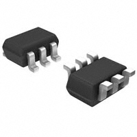
H1
TS
Pin connections
(top view)
IN 1
6 VCC
GND 2
5 EN
(Enable)
SAG 3
4 OUT
The TSH120 is a single operator available in a
tiny SC70 plastic package for space saving.
■
Camera phones
■
Digital still camera
■
Digital video camera
■
Set-top box and DVD video outputs
The TSH120 is a video buffer that includes a
voltage feedback amplifier with an internal gain of
6dB, rail-to-rail output, internal input biasing and
SAG correction. A power down function offers a
sleep mode with ultra low consumption.
The TSH120 also features an internal
reconstruction filter in order to attenuate the
parasitic 27MHz frequency from the clock of the
video DAC.
August 2007
Rev 3
1/13
www.st.com
13
�Absolute maximum ratings
1
TSH120
Absolute maximum ratings
Table 1.
Absolute maximum ratings
Symbol
VCC
Vin
Parameter
Supply voltage (1)
(2)
Input voltage range
Value
Unit
6
V
2
V
Toper
Operating free air temperature range
-40 to +105
°C
Tstg
Storage temperature
-65 to +150
°C
Maximum junction temperature
150
°C
Rthja
Thermal resistance junction to ambient
430
°C/W
Rthjc
Thermal resistance junction to case
58
°C/W
Pmax
Maximum power dissipation(3) for Tj=150°C
Ta=+25°C
Ta=+85°C
290
150
mW
HBM: human body model (4)
except pin-4
pin-4
2
1.5
kV
MM: machine model (5)
200
V
Latch-up immunity
200
mA
Tj
)
s
(
t
c
u
d
o
)
r
s
(
P
t
c
e
t
u
e
d
l
o
o
r
s
P
b
e
O
t
e
l
)
o
s
(
s
t
b
c
u
O
d
o
)
r
s
P
(
t
c
e
t
u
e
l
d
o
o
r
s
P
b
O
e
t
e
l
o
s
b
O
ESD
1. All voltage values are measured with respect to the ground pin.
2. The magnitude of input and output voltage must never exceed VCC +0.3V.
3. Short-circuits can cause excessive heating. Destructive dissipation can result from short-circuits on
amplifiers.
4. Human body model: A 100pF capacitor is charged to the specified voltage, then discharged through a
1.5kΩ resistor between two pins of the device. This is done for all couples of connected pin combinations
while the other pins are floating.
5. Machine model: A 200pF capacitor is charged to the specified voltage, then discharged directly between
two pins of the device with no external series resistor (internal resistor < 5Ω). This is done for all couples of
connected pin combinations while the other pins are floating. This is a minimum value.
Table 2.
Operating conditions
Symbol
VCC
Parameter
Supply voltage (1)
1. Tested in full production at +2.5V and +3.3V single supply voltage.
2/13
Value
Unit
2.2 to 5.5
V
�TSH120
Electrical characteristics
2
Electrical characteristics
Table 3.
Electrical characteristics for VCC = +2.5V and +3.3V, Tamb = 25°C (unless otherwise
specified)
Symbol
Parameter
Test conditions
Min.
Typ.
Max.
Unit
94
129
158
mV
DC performance
Vdc
Output DC level shift
RL = 150Ω
Tmin ≤ Tamb ≤ Tmax
μV/°C
403
VCC= +3.3V
Tmin ≤ Tamb ≤ Tmax
-880
-550
-650
VCC= +2.5V
Tmin ≤ Tamb ≤ Tmax
-840
-550
-620
5.95
6.1
6.05
)
s
(
t
c
u
d
o
)
r
s
(
P
t
c
e
t
u
e
d
l
o
o
r
s
P
b
e
O
t
e
l
)
o
s
(
s
t
b
c
u
O
d
o
)
r
s
P
(
t
c
e
t
u
e
l
d
o
o
r
s
P
b
O
e
t
e
l
o
s
b
O
Iib
Input bias current
G
Internal voltage gain
Vin=1V
Tmin ≤ Tamb ≤ Tmax
Power supply rejection ratio
20 log (ΔVCC/ΔVout)
ΔVCC=±100mV at 1MHz
55
No load, Vin=+0.5V
VCC=+3.3V
Tmin ≤ Tamb ≤ Tmax
5.8
6.7
6.6
mA
No load, Vin=+0.5V
VCC=+2.5V
Tmin ≤ Tamb ≤ Tmax
5.8
6.7
6.3
mA
PSRR
ICC
Current consumption
nA
6.2
dB
dB
Enable/standby (EN pin)
ISTBY
Consumption in standby mode
VCC=+3.3V
4
VCC=+2.5V
2
VSTBY-low
Standby low level
Standby mode
VSTBY-high
Standby high level
Enable mode
+0.3
+0.8
μA
V
V
Ton
Time from standby to enable
5
μs
Toff
Time from enable to standby
5
μs
Dynamic performance and output characteristics
Vout=2Vpp, RL = 150Ω
VCC=+3.3V, F=4.5MHz
Tmin ≤ Tamb ≤ Tmax
FR
VOH
Frequency response
High level output voltage
-0.4
Vout=2Vpp, RL = 150Ω
VCC=+2.5V, F=4.5MHz
-0.1
-0.48
0
VCC=+3.3V, F=27MHz
Tmin ≤ Tamb ≤ Tmax
-20
-25
-23
VCC=+3.3V, RL=150Ω
VCC=+2.5V, RL=150Ω
3.13
2.36
3.21
2.42
0.4
dB
V
3/13
�Electrical characteristics
Table 3.
Electrical characteristics for VCC = +2.5V and +3.3V, Tamb = 25°C (unless otherwise
specified) (continued)
Symbol
VOL
TSH120
Parameter
Low level output voltage
Test conditions
Vin= -100mV, RL = 150Ω
VCC=+3.3V
Tmin ≤ Tamb ≤ Tmax
Min.
Typ.
Max.
5
5.6
34
Unit
mV
Vin= -100mV, RL = 150Ω
VCC=+2.5V
Tmin ≤ Tamb ≤ Tmax
5
5.5
VCC=+3.3V, output to GND
30
33
Iout
Isource
ΔG
Differential gain
VCC=+3.3V, RL = 150Ω
0.5
%
Δφ
Differential phase
VCC=+3.3V, RL = 150Ω
0.5
°
Gd
Group delay
10kHz to 6MHz
Total output noise
F = 100kHz, no load
25
nV/√Hz
Output signal to noise ratio
VCC=+3.3V, RL = 150Ω
Vout=2Vpp from 0 to 6MHz
60
dB
mA
)
s
(
t
c
u
d
o
)
r
s
(
P
t
c
e
t
u
e
d
l
o
o
r
s
P
b
e
O
t
e
l
)
o
s
(
s
t
b
c
u
O
d
o
)
r
s
P
(
t
c
e
t
u
e
l
d
o
o
r
s
P
b
O
e
t
e
l
o
s
b
O
10 (1)
ns
Noise
eN
SNR
1. Guaranteed by design. The parameter is not tested.
4/13
�TSH120
Figure 1.
Electrical characteristics
Frequency response
Figure 2.
7.0
10
5
6.8
0
-5
Vcc=+3.3V
Load=150Ω
6.6
Vcc=+5V
-10
6.4
-15
Vcc=+3.3V
-20
Vcc=+2.5V
Gain (dB)
Gain (dB)
Gain flatness
-25
-30
6.2
6.0
5.8
-35
-40
5.6
-45
5.4
-50
)
s
(
t
c
u
d
o
)
r
s
(
P
t
c
e
t
u
e
d
l
o
o
r
s
P
b
e
O
t
e
l
)
o
s
(
s
t
b
c
u
O
d
o
)
r
s
P
(
t
c
e
t
u
e
l
d
o
o
r
s
P
b
O
e
t
e
l
o
s
b
O
5.2
-55
-60
100k
1M
10M
5.0
100k
100M
27MHz
1M
Frequency (Hz)
Figure 3.
Total input noise vs. frequency
Figure 4.
500
No load
Input to GND
Vcc=+3.3V
Distortion (dB)
-30
300
200
100
Vcc=+3.3V
Vicm=0.5V
F=1MHz
Load=150Ω
-40
H2
-50
-60
100
1k
10k
100k
1M
10M
-70
0.0
H3
0.5
1.0
1.5
2.0
2.5
3.0
3.5
4.0
Output Amplitude (Vp-p)
Frequency (Hz)
Figure 5.
Output voltage swing vs. supply
5.0
4.5
Output swing (Vp-p)
en (nV/VHz)
Distortion on 150Ω load
-20
400
0
10
10M
Frequency (Hz)
F=1MHz
Load=150Ω
4.0
3.5
3.0
2.5
2.0
1.5
2.0
2.5
3.0
3.5
4.0
4.5
5.0
5.5
Vcc (V)
5/13
�Electrical characteristics
Figure 6.
TSH120
Quiescent current vs. supply
Figure 7.
150
6.5
145
Output DC shift (mV)
7.0
Icc (mA)
6.0
5.5
5.0
no input signal
Load=150Ω
4.5
Output DC shift vs. VCC
140
135
130
Vin=+0.5Vdc
Load=150Ω
125
)
s
(
t
c
u
d
o
)
r
s
(
P
t
c
e
t
u
e
d
l
o
o
r
s
P
b
e
O
t
e
l
)
o
s
(
s
t
b
c
u
O
d
o
)
r
s
P
(
t
c
e
t
u
e
l
d
o
o
r
s
P
b
O
e
t
e
l
o
s
b
O
4.0
2.0
2.5
3.0
3.5
4.0
4.5
5.0
120
2.0
5.5
2.5
3.0
3.5
Vcc (V)
Figure 8.
Standby - Output Ton (VCC=+3.3V)
Figure 9.
5.0
5.5
Out
Pin-5
Pin-5
Figure 10. Flatness vs. Tamb
Figure 11. Ibias vs. Tamb
0.0
0.5
Vout=2Vp-p
Load=150Ω
-0.1
0.3
Vcc=+2.5V and +3.3V
Load=150Ω
-0.2
0.2
Vcc=+2.5V
0.1
IBIAS (μA)
Flatness@4.5MHz (dB)
4.5
Standby - Output Toff (VCC=+3.3V)
Out
0.4
4.0
Vcc (V)
0.0
-0.1
-0.2
-0.3
-0.4
-0.5
Vcc=+3.3V
-0.3
-0.6
-0.4
-0.5
-40
-20
0
20
40
Temperature (°C)
6/13
60
80
-0.7
-40
-20
0
20
40
Temperature (°C)
60
80
�TSH120
Electrical characteristics
Figure 12. Voltage gain vs. Tamb
Figure 13. Filter attenuation vs. Tamb
6.10
-20
-22
Attenuation@27MHz (dB)
6.05
Gain (dB)
6.00
5.95
5.90
5.85
Vcc=+2.5V and +3.3V
Load=150Ω
Load=150Ω
-24
-26
-28
Vcc=+3.3V
-30
-32
-34
-36
Vcc=+2.5V
)
s
(
t
c
u
d
o
)
r
s
(
P
t
c
e
t
u
e
d
l
o
o
r
s
P
b
e
O
t
e
l
)
o
s
(
s
t
b
c
u
O
d
o
)
r
s
P
(
t
c
e
t
u
e
l
d
o
o
r
s
P
b
O
e
t
e
l
o
s
b
O
5.80
-40
-20
0
-38
20
40
60
-40
-40
80
-20
Temperature (°C)
0
20
40
60
80
Temperature (°C)
Figure 14. Supply current vs. Tamb
Figure 15. Output DC shift vs. Tamb
7.0
180
Vcc=+2.5V and +3.3V
Load=150Ω
170
6.5
160
Output DCshift (V)
6.0
ICC (mA)
5.5
5.0
4.5
4.0
3.5
3.0
-40
0
140
130
120
110
100
Vcc=+2.5V and +3.3V
no input signal
no Load
-20
150
90
20
40
60
80
-40
80
-20
0
Temperature (°C)
20
40
60
80
Temperature (°C)
Figure 16. VOH vs. Tamb
Figure 17. VOL vs. Tamb
4.0
10
Load=150Ω
9
8
3.5
7
VOL (mV)
VOH (V)
Vcc=+3.3V
3.0
6
5
Vcc=+3.3V
4
3
Vcc=+2.5V
2.5
2
Vcc=+2.5V
2.0
-40
-20
1
0
20
40
Temperature (°C)
60
80
0
-40
Load=150Ω
-20
0
20
40
60
80
Temperature (°C)
7/13
�Implementation in the application
3
TSH120
Implementation in the application
This section explains how the TSH120 video buffer operates in a typical application.
On the input, a DC level shifter optimizes the position of the video signal with no clamping
on the output rails. The filter is a reconstruction filter. It is used to attenuate the DAC’s
sampling frequency which causes a parasitic signal in the video spectrum (typically at
27MHz in the case of standard video). This function must be achieved while keeping a low
group delay.
On the output, the SAG correction decreases Cout while keeping a very low frequency pole
(see Figure 18). Nevertheless, the output can be directly connected to the line without any
capacitor. In this case, both OUT and SAG pins are connected together and the equivalent
gain of the buffer remains 6dB (see Figure 19).
)
s
(
t
c
u
d
o
)
+2.2V to +5.5V
r
s
(
P
t
c
e
t
u
e
d
l
+
o
o
r
s
P
b
e
O
t
e
l
)
o
s
(
s
t
b
c
u
O
d
o
)
r
s
P
(
t
c
e
t
u
e
l
d +2.2V to +5.5V
o
o
r
s
P
b
O
e
t
e
l
+
o
s
b
O
Figure 18. Schematic diagram with output capacitor
6
DC shifter
Video
DAC
1
LPF
TV
5 Shutdown
Cout
33µF
Rail-to-rail
75
75
cable
4
3rd order
1Vpp
75
1Vpp
3
SAG 22µF
2Vpp
2
Figure 19. Schematic diagram without output capacitor
6
DC shifter
Video
DAC
1
LPF
3rd
TV
5 Shutdown
75
Rail-to-rail
4
order
cable
1Vpp
75
1Vpp
3
SAG
2
8/13
75
2Vpp
�TSH120
4
Power supply considerations
Power supply considerations
Correct power supply bypassing is very important for optimizing performance in the highfrequency range. A bypass capacitor greater than 10μF is necessary to minimize the
distortion. For better quality bypassing at higher frequencies, a capacitor of 10nF must be
added as close as possible to the IC pin of VCC.
Figure 20. Circuit for power supply bypassing
+VCC
CLF=10 F
+
)
s
(
t
c
u
d
o
)
r
s
(
P
t
c
e
t
u
e
d
l
o
o
r
s
P
b
e
O
t
e
l
)
o
s
(
s
t
b
c
u
O
d
o
)
r
s
P
(
t
c
e
t
u
e
l
d
o
o
r
s
P
b
O
e
t
e
l
o
s
b
O
CHF=10nF
TSH120
Figure 21 shows the noise supply rejection improvement with bypass capacitors expressed
by:
20 log (ΔVout / ΔVCC).
Figure 21. Noise supply rejection
0
Noise supply rejection (dB)
-10
-20
-30
Vcc=+3.3Vdc+0.2Vac
Load=150Ω
CLF=10uF
CHF=100nF
-40
-50
-60
-70
-80
-90
-100
10k
100k
1M
10M
100M
Frequency (Hz)
9/13
�Package information
5
TSH120
Package information
In order to meet environmental requirements, STMicroelectronics offers these devices in
ECOPACK® packages. These packages have a lead-free second level interconnect. The
category of second level interconnect is marked on the package and on the inner box label,
in compliance with JEDEC Standard JESD97. The maximum ratings related to soldering
conditions are also marked on the inner box label. ECOPACK is an STMicroelectronics
trademark. ECOPACK specifications are available at: www.st.com.
Figure 22. SC70-6 (or SOT323-6) package footprint (in millimeters)
)
s
(
t
c
u
d
o
)
r
s
(
P
t
c
e
t
u
e
d
l
o
o
r
s
P
b
e
O
t
e
l
)
o
s
(
s
t
b
c
u
O
d
o
)
r
s
P
(
t
c
e
t
u
e
l
d
o
o
r
s
P
b
O
e
t
e
l
o
s
b
O
0.65
1.05
0.80
2.90
0.40
10/13
�TSH120
Package information
Figure 23. SC70-6 (or SOT323-6) package mechanical data
Dimensions
Ref
Millimeters
Min
Typ
Mils
Max
Min
Typ
Max
A
0.80
1.10
31.5
43.3
A1
0
0.10
0
3.9
A2
0.80
1.00
31.5
39.3
b
0.15
0.30
5.9
11.8
c
0.10
0.18
3.9
7.0
D
1.80
2.20
70.8
86.6
E
1.15
1.35
45.2
43.1
)
s
(
t
c
u
d
o
)
r
s
(
P
t
c
e
t
u
e
d
l
o
o
r
s
P
b
e
O
t
e
l
)
o
s
(
s
t
b
c
u
O
d
o
)
r
s
P
(
t
c
e
t
u
e
l
d
o
o
r
s
P
b
O
e
t
e
l
o
s
b
O
e
0.65
25.6
2.4
70.8
94.5
L
0.10
0.40
3.9
15.7
Q1
0.10
0.40
3.9
15.7
A
1.8
A2
HE
D
A1
E
HE
L
b
Q1
C
e
e
11/13
�Ordering information
6
TSH120
Ordering information
Table 4.
Order codes
Part number
Temperature
range
Package
Packaging
Marking
TSH120ICT
-40°C to +85°C
SC70-6
(or SOT323-6)
Tape & reel
K30
)
s
(
t
c
u
d
o
)
r
s
(
P
t
c
e
t
u
e
d
l
o
o
r
s
P
b
e
O
t
e
l
)
o
s
(
s
t
b
c
u
O
d
o
)
r
s
P
(
t
c
e
t
u
e
l
d
o
o
r
s
P
b
O
e
t
e
l
o
s
b
O
7
Revision history
Table 5.
12/13
Document revision history
Date
Revision
Changes
29-May-2007
1
Initial version, preliminary data.
20-Jun-2007
2
First complete datasheet.
21-Aug-2007
3
Corrected pinout diagram on cover page (SAG missing).
�TSH120
)
s
(
t
c
u
d
o
)
r
s
(
P
t
c
e
t
u
e
d
l
o
o
r
s
P
b
e
O
t
e
l
)
o
s
(
s
t
b
c
u
O
d
o
)
r
s
P
(
t
c
e
t
u
e
l
d
o
o
r
s
P
b
O
e
t
e
l
o
s
b
O
Please Read Carefully:
Information in this document is provided solely in connection with ST products. STMicroelectronics NV and its subsidiaries (“ST”) reserve the
right to make changes, corrections, modifications or improvements, to this document, and the products and services described herein at any
time, without notice.
All ST products are sold pursuant to ST’s terms and conditions of sale.
Purchasers are solely responsible for the choice, selection and use of the ST products and services described herein, and ST assumes no
liability whatsoever relating to the choice, selection or use of the ST products and services described herein.
No license, express or implied, by estoppel or otherwise, to any intellectual property rights is granted under this document. If any part of this
document refers to any third party products or services it shall not be deemed a license grant by ST for the use of such third party products
or services, or any intellectual property contained therein or considered as a warranty covering the use in any manner whatsoever of such
third party products or services or any intellectual property contained therein.
UNLESS OTHERWISE SET FORTH IN ST’S TERMS AND CONDITIONS OF SALE ST DISCLAIMS ANY EXPRESS OR IMPLIED
WARRANTY WITH RESPECT TO THE USE AND/OR SALE OF ST PRODUCTS INCLUDING WITHOUT LIMITATION IMPLIED
WARRANTIES OF MERCHANTABILITY, FITNESS FOR A PARTICULAR PURPOSE (AND THEIR EQUIVALENTS UNDER THE LAWS
OF ANY JURISDICTION), OR INFRINGEMENT OF ANY PATENT, COPYRIGHT OR OTHER INTELLECTUAL PROPERTY RIGHT.
UNLESS EXPRESSLY APPROVED IN WRITING BY AN AUTHORIZED ST REPRESENTATIVE, ST PRODUCTS ARE NOT
RECOMMENDED, AUTHORIZED OR WARRANTED FOR USE IN MILITARY, AIR CRAFT, SPACE, LIFE SAVING, OR LIFE SUSTAINING
APPLICATIONS, NOR IN PRODUCTS OR SYSTEMS WHERE FAILURE OR MALFUNCTION MAY RESULT IN PERSONAL INJURY,
DEATH, OR SEVERE PROPERTY OR ENVIRONMENTAL DAMAGE. ST PRODUCTS WHICH ARE NOT SPECIFIED AS "AUTOMOTIVE
GRADE" MAY ONLY BE USED IN AUTOMOTIVE APPLICATIONS AT USER’S OWN RISK.
Resale of ST products with provisions different from the statements and/or technical features set forth in this document shall immediately void
any warranty granted by ST for the ST product or service described herein and shall not create or extend in any manner whatsoever, any
liability of ST.
ST and the ST logo are trademarks or registered trademarks of ST in various countries.
Information in this document supersedes and replaces all information previously supplied.
The ST logo is a registered trademark of STMicroelectronics. All other names are the property of their respective owners.
© 2007 STMicroelectronics - All rights reserved
STMicroelectronics group of companies
Australia - Belgium - Brazil - Canada - China - Czech Republic - Finland - France - Germany - Hong Kong - India - Israel - Italy - Japan Malaysia - Malta - Morocco - Singapore - Spain - Sweden - Switzerland - United Kingdom - United States of America
www.st.com
13/13
�