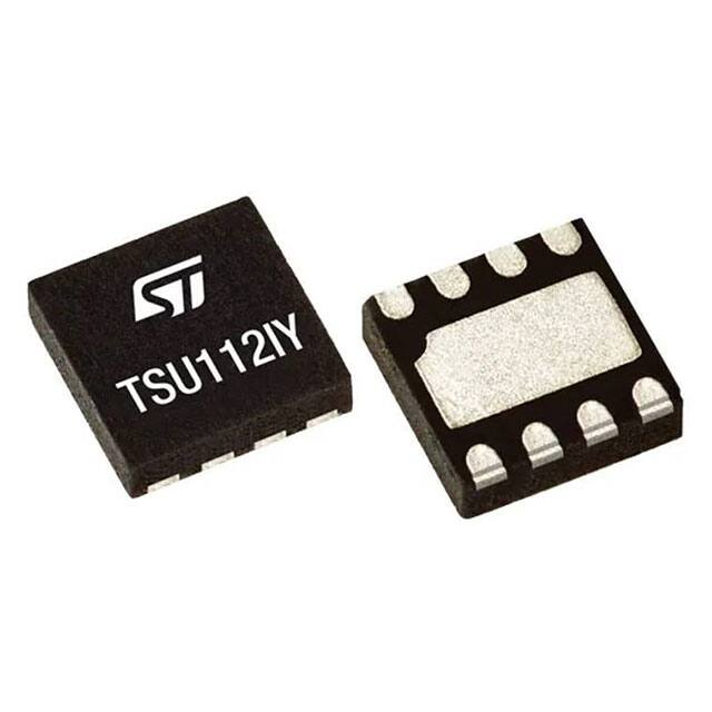
TSU112IY
Datasheet
Automotive grade, nanopower (920 nA), high accuracy (150 μV) 5 V CMOS
operational amplifier
Features
•
•
AEC-Q100 qualified
Sub-micro ampere current consumption: Icc = 920 nA typ. at 25 °C
•
Low offset voltage: 150 µV max. at 25 °C, 400 µV max. over full temperature
range (-40 to 125 °C)
Low noise over 0.1 to 10 Hz bandwidth: 4.6 µVpp
Low supply voltage: 1.5 V to 5.5 V
Rail-to-rail input and output
Gain bandwidth product: 9 kHz typ.
Low input bias current: 10 pA max. at 25 °C
High tolerance to ESD: 4 kV HBM
More than 25 years of typical equivalent lifetime supplied by a 220 mA.h
CR2032 coin type Lithium battery
High accuracy without calibration
Tolerance to power supply transient drops
•
•
•
•
•
•
•
•
•
Applications
•
Product status link
TSU112IY
Related products
See TSU101,
TSU102 and
TSU104
For further power
savings
See TSZ121,
TSZ122 and
TSZ124
For increased
accuracy
•
•
•
Battery management system: ultra-low power op-amp detects when battery is
charging/discharging and wakes up CPU
On-board chargers
Signal conditioning for energy harvesting
Wireless chargers
Description
The TSU112IY operational amplifier (op-amp) offers an ultra low-power consumption
per channel of 920 nA typical and 1.3 µA maximum when supplied by 3.3 V.
Combined with a supply voltage range of 1.5 V to 5.5 V, these features allow the
TSU112IY to be efficiently supplied by a coin type Lithium battery or a regulated
voltage in low-power applications.
The high accuracy of 150 µV max. and 9 kHz gain bandwidth make the TSU112IY
ideal for sensor signal conditioning, battery management system, on-board (OBC)
and wireless chargers.
DS13616 - Rev 2 - July 2021
For further information contact your local STMicroelectronics sales office.
www.st.com
�TSU112IY
Package pin connections
1
Package pin connections
Figure 1. Pin connections for each package (top view)
DFN8 2x2
MiniSO8
1. The exposed pad of the DFN8 2x2 can be connected to VCC- or left floating.
DS13616 - Rev 2
page 2/31
�TSU112IY
Absolute maximum ratings and operating conditions
2
Absolute maximum ratings and operating conditions
Table 1. Absolute maximum ratings (AMR)
Symbol
Parameter
VCC
Supply voltage (1)
Vid
Differential input voltage (2)
Vin
Input voltage (3)
Iin
(4)
Tstg
Tj
Rthja
Input current
Value
6
±VCC
V
(VCC -) - 0.2 to (VCC +) + 0.2
10
Storage temperature
-65 to 150
Maximum junction temperature
150
Thermal resistance junction-to-ambient (5) (6)
DFN8 2x2
57
MiniSO8
190
HBM: human body model (7)
ESD
Unit
CDM: charged device model
mA
°C
°C/W
4000
(8)
V
1500
Latch-up immunity (9)
200
mA
1. All voltage values, except the differential voltage, are with respect to the network ground terminal.
2. The differential voltage is the non-inverting input terminal with respect to the inverting input terminal.
3. (VCC+) - Vin must not exceed 6 V, Vin - (VCC-) must not exceed 6 V.
4. The input current must be limited by a resistor in-series with the inputs.
5. Rth are typical values.
6. Short-circuits can cause excessive heating and destructive dissipation.
7. HBM test according to the standard AEC-Q100-002 and related to ESDA/JEDEC JS-001-2017.
8. The test CDM is performed in accordance with the standard AEC-Q100-011 and related to ESDA/JEDEC JS-002-2018.
9. Related to JEDEC JESD78E Apr. 2016.
Table 2. Operating conditions
Symbol
DS13616 - Rev 2
Parameter
VCC
Supply voltage
Vicm
Common-mode input voltage range
Toper
Operating free-air temperature range
Value
1.5 to 5.5
(VCC-) - 0.1 to (VCC+) + 0.1
-40 to 125
Unit
V
°C
page 3/31
�TSU112IY
Electrical characteristics
3
Electrical characteristics
Table 3. Electrical characteristics at (VCC+) = 1.8 V with (VCC- ) = 0 V, Vicm = VCC/2, Tamb = 25 °C, and RL = 1 MΩ
connected to VCC/2 (unless otherwise specified)
Symbol
Parameter
Conditions
Min.
Typ.
Max.
Unit
DC performance
Vio
Input offset voltage
ΔVio/ΔT
Input offset voltage drift
Iio
Input offset current (1)
Iib
Input bias current (1)
Common mode rejection ratio,
CMR
20 log (ΔVicm/ΔVio),
Vicm = 0 to 1.8 V
Avd
Large signal voltage gain,
Vout = 0.2 V to (VCC+) - 0.2 V
T = 25 °C
150
-40 °C < T< 125 °C
400
-40 °C < T< 125 °C
2.5
T = 25 °C
1
-40 °C < T< 125 °C
1
-40 °C < T< 125 °C
76
-40 °C < T< 125 °C
71
RL = 100 kΩ, T = 25 °C
95
RL = 100 kΩ,
VOH
99
11
RL = 10 kΩ,
9
RL = 10 kΩ,
Vout = VCC ,
Iout
VΙD = -200 mV
Output source current,
Vout = 0 V,
VΙD = 200 mV
ICC
T = 25 °C
2.8
-40 °C < T< 85 °C
1.5
T = 25 °C
2
-40 °C < T< 125 °C
1.5
Supply current (per channel),
no load,
T = 25 °C
Vout = VCC/2
-40 °C < T< 125 °C
25
mV
40
-40 °C < T< 125 °C
Output sink current,
25
40
RL = 10 kΩ, T = 25 °C
Low-level output voltage
dB
120
-40 °C < T< 125 °C
VOL
pA
82
RL = 10 kΩ, T = 25 °C
High-level output voltage,
(drop from VCC+)
10
50
T = 25 °C
-40 °C < T< 125 °C
μV/°C
10
50
T = 25 °C
µV
5
mA
4
840
1300
1580
nA
AC performance
GBP
Gain bandwidth product
9
Fu
Unity gain frequency
5.5
Φm
Phase margin
Gm
Gain margin
SRp
Slew rate (10 % to 90 %)
DS13616 - Rev 2
RL = 1 MΩ, CL = 60 pF
RL = 1 MΩ, CL = 60 pF,
Vout = 0.3 V to (VCC+) - 0.3 V
0.8
kHz
70
degrees
30
dB
1.8
V/ms
page 4/31
�TSU112IY
Electrical characteristics
Symbol
Parameter
SRn
Slew rate (10 % to 90 %)
en
Equivalent input noise voltage
ʃen
Low-frequency, peak-to-peak
input noise
trecP
Overload recovery time (from
positive rail)
trecP
Overload recovery time (from
negative rail)
Conditions
Min.
Typ.
1.2
3.0
V/ms
f = 100 Hz
220
nV/√Hz
Bandwidth: f = 0.1 to 10 Hz
4.6
µVpp
100 mV from rail in comparator,
RL = 100 kΩ,
220
µs
430
µs
RL = 1 MΩ, CL = 60 pF,
Vout = 0.3 V to (VCC+) - 0.3 V
Max.
Unit
VΙD = ±1 V, -40 °C < T< 125 °C
100 mV from rail in comparator,
RL = 100 kΩ,
VΙD = ±1 V, -40 °C < T< 125 °C
1. Guaranteed by design
Table 4. Electrical characteristics at (VCC+) = 3.3 V with (VCC-) = 0 V, Vicm = VCC/2, Tamb = 25 °C, and RL = 1 MΩ
connected to V CC/2 (unless otherwise specified)
Symbol
Parameter
Conditions
Min.
Typ.
Max.
Unit
DC performance
Vio
Input offset voltage
ΔVio/ΔT
Input offset voltage drift
Iio
Input offset current (1)
Iib
CMR
Avd
Input bias current (1)
VOL
400
-40 °C < T< 125 °C
2.5
T = 25 °C
1
-40 °C < T< 125 °C
T = 25 °C
1
-40 °C < T< 125 °C
-40 °C < T< 125 °C
76
RL = 100 kΩ, T = 25 °C
100
RL = 100 kΩ, -40 °C < T< 125 °C
88
High-level output voltage,
(drop from VCC+)
Low-level output voltage
VΙD = -200 mV
Output source current,
Vout = 0 V,
VΙD = 200 mV
μV/°C
10
pA
50
20 log (ΔVicm/ΔVio), Vicm = 0
to 3.3 V
Large signal voltage gain,
Vout = 0.2 V to
µV
10
50
81
Vout = VCC ,
DS13616 - Rev 2
-40 °C < T< 125 °C
T = 25 °C
Output sink current,
Iout
150
Common mode rejection ratio,
(VCC+) - 0.2 V
VOH
T = 25 °C
RL = 10 kΩ, T = 25 °C
102
dB
128
11
RL = 10 kΩ, -40 °C < T< 125 °C
25
40
RL = 10 kΩ, T = 25 °C
9
RL = 10 kΩ, -40 °C < T< 125 °C
25
mV
40
T = 25 °C
12
-40 °C < T< 125 °C
6
T = 25 °C
9
-40 °C < T< 125 °C
5
22
17
mA
page 5/31
�TSU112IY
Electrical characteristics
Symbol
Parameter
Conditions
Supply current (per channel),
no load,
T = 25 °C
ICC
Vout = VCC/2
-40 °C < T< 125 °C
Min.
Typ.
Max.
920
1300
Unit
nA
1650
AC performance
GBP
Gain bandwidth product
9
Fu
Unity gain frequency
5.5
Φm
Phase margin
Gm
Gain margin
SRp
Slew rate (10 % to 90 %)
SRn
Slew rate (10 % to 90 %)
en
Equivalent input noise voltage
ʃen
Low-frequency, peak-to-peak
input noise
trec P
Overload recovery time (from
positive rail)
Overload recovery time (from
negative rail)
trec N
RL = 1 MΩ, CL = 60 pF
kHz
70
degrees
30
dB
0.9
1.8
V/ms
1.5
3.0
V/ms
f = 100 Hz
200
nV/√Hz
Bandwidth: f = 0.1 to 10 Hz
4.6
µVpp
100 mV from rail in comparator,
RL = 100 kΩ,
420
µs
880
µs
RL = 1 MΩ, CL = 60 pF,
Vout = 0.3 V to (VCC+) - 0.3 V
RL = 1 MΩ, CL = 60 pF,
Vout = 0.3 V to (VCC+) - 0.3 V
VΙD = ±1 V, -40 °C < T< 125 °C
100 mV from rail in comparator,
RL = 100 kΩ,
VΙD = ±1 V, -40 °C < T< 125 °C
1. Guaranteed by design
Table 5. Electrical characteristics at (VCC+) = 5 V with (VCC-) = 0 V, Vicm = VCC/2, Tamb = 25 °C, and RL = 1 MΩ connected
to V CC/2 (unless otherwise specified)
Symbol
Parameter
Conditions
Min. Typ. Max.
Unit
DC performance
Vio
Input offset voltage
ΔVio/ΔT
Input offset voltage drift
Iio
Input offset current (1)
Iib
Input bias current (1)
CMR
Common mode rejection ratio, 20 log (ΔVicm/ΔVio), Vicm = 0 to 5 V
SVR
Avd
DS13616 - Rev 2
T = 25 °C
150
-40 °C < T< 125 °C
400
-40 °C < T< 125 °C
2.5
T = 25 °C
1
-40 °C < T< 125 °C
1
-40 °C < T< 125 °C
μV/°C
10
50
T = 25 °C
µV
10
pA
50
T = 25 °C
85
-40 °C < T< 125 °C
80
Supply voltage rejection ratio, VCC = 1.5 to 5.5 V,
T = 25 °C
89
Vicm = 0 V
-40 °C < T< 125 °C
84
Large signal voltage gain, Vout = 0.2 V to
RL = 100 kΩ, T = 25 °C
105
(VCC+) - 0.2 V
RL = 100 kΩ, -40 °C < T< 125 °C
92
106
107
dB
132
page 6/31
�TSU112IY
Electrical characteristics
Symbol
Parameter
VOH
High-level output voltage, (drop from VCC+)
VOL
Min. Typ. Max.
RL = 10 kΩ, T = 25 °C
12
RL = 10 kΩ, -40 °C < T< 125 °C
Low-level output voltage
10
RL = 10 kΩ, -40 °C < T< 125 °C
Iout
Output source current, Vout = 0 V, VΙD = 200 mV
25
mV
40
T = 25 °C
30
-40 °C < T< 125 °C
15
T = 25 °C
9
-40 °C < T< 125 °C
18
T = 25 °C
Supply current (per channel), no load, Vout = VCC/2
Unit
25
40
RL = 10 kΩ, T = 25°C
Output sink current, Vout = VCC , VΙD = -200 mV
ICC
Conditions
45
mA
39
1000 1400
-40 °C < T< 125 °C
2000
nA
AC performance
GBP
Gain bandwidth product
9
Fu
Unity gain frequency
6
Φm
Phase margin
Gm
Gain margin
SRp
Slew rate (10 % to 90 %)
SRn
Slew rate (10 % to 90 %)
en
Equivalent input noise voltage
ʃen
Low-frequency, peak-to-peak input noise
RL = 1 MΩ, CL = 60 pF
kHz
70
degrees
30
dB
0.9
1.9
V/ms
1.5
3.1
V/ms
f = 100 Hz
220
nV/√Hz
Bandwidth: f = 0.1 to 10 Hz
4.6
µVpp
650
µs
1300
µs
RL = 1 MΩ, CL = 60 pF,
Vout = 0.3 V to (VCC+) - 0.3 V
RL = 1 MΩ, CL = 60 pF,
Vout = 0.3 V to (VCC+) - 0.3 V
100 mV from rail in comparator,
trec P
Overload recovery time (from positive rail)
RL = 100 kΩ,
VΙD = ±1 V -40 °C < T< 125 °C
100 mV from rail in comparator,
trecN
Overload recovery time (from negative rail)
RL = 100 kΩ,
VΙD = ±1 V, -40 °C < T< 125 °C
1. Guaranteed by design
DS13616 - Rev 2
page 7/31
�TSU112IY
Electrical characteristic curves
4
DS13616 - Rev 2
Electrical characteristic curves
Figure 2. Supply current vs. supply voltage at low
VICM
Figure 3. Supply current vs. supply voltage at high
VICM
Figure 4. Supply current vs. supply voltage at mid
VICM
Figure 5. Supply current vs. input common-mode
voltage
page 8/31
�TSU112IY
Electrical characteristic curves
DS13616 - Rev 2
Figure 6. Input offset voltage vs. input commonmode voltage
Figure 7. Input offset voltage distribution
Figure 8. Input offset voltage temperature
coefficient distribution from -40 °C to 25 °C
Figure 9. Input offset voltage temperature
coefficient distribution from 25 °C to 125 °C
page 9/31
�TSU112IY
Electrical characteristic curves
Figure 10. Input offset voltage vs. temperature at
3.3 V
Figure 12. High level output voltage (drop from
VCC+)
DS13616 - Rev 2
Figure 11. Input bias current vs. temperature at mid
VICM
Figure 13. Low level output voltage
page 10/31
�TSU112IY
Electrical characteristic curves
DS13616 - Rev 2
Figure 14. Output characteristics at 1.5 V supply
voltage
Figure 15. Output characteristics at 1.8 V supply
voltage
Figure 16. Output characteristics at 3.3 V supply
voltage
Figure 17. Output characteristics at 5 V supply
voltage
page 11/31
�TSU112IY
Electrical characteristic curves
DS13616 - Rev 2
Figure 18. Output characteristics at 5.5 V supply
voltage
Figure 19. Output saturation with a sinewave on the
input
Figure 20. Output saturation with a square wave on
the input
Figure 21. Phase reversal free
page 12/31
�TSU112IY
Electrical characteristic curves
DS13616 - Rev 2
Figure 22. Recovery time from negative saturation
vs. supply voltage
Figure 23. Recovery time from positive saturation
vs. supply voltage
Figure 24. Slew rate vs. supply voltage
Figure 25. Output swing vs. input signal frequency
page 13/31
�TSU112IY
Electrical characteristic curves
DS13616 - Rev 2
Figure 26. Triangulation of a sine wave
Figure 27. Large signal response at 3.3 V supply
voltage
Figure 28. Small signal response at 3.3 V supply
voltage
Figure 29. Overshoot vs. capacitive load at 3.3 V
supply voltage
page 14/31
�TSU112IY
Electrical characteristic curves
Figure 30. Over/under shoot vs supply voltage
Figure 32. Bode diagram at 1.8 V supply voltage
Figure 34. Bode diagram at 5 V supply voltage
DS13616 - Rev 2
Figure 31. Bode diagram at 1.5 V supply voltage
Figure 33. Bode diagram at 3.3 V supply voltage
Figure 35. Bode diagram at 5.5 V supply voltage
page 15/31
�TSU112IY
Electrical characteristic curves
DS13616 - Rev 2
Figure 36. In series resistor Riso vs. capacitive
load
Figure 37. Noise amplitude on 0.1 to 10 Hz freq.
range
Figure 38. Noise vs. frequency for different
common mode input voltages
Figure 39. Noise vs. frequency for different power
supply voltages
page 16/31
�TSU112IY
Electrical characteristic curves
Figure 40. Gain bandwidth product vs. input common mode voltage
DS13616 - Rev 2
page 17/31
�TSU112IY
Application information
5
Application information
5.1
Nanopower applications
The TSU112IY can operate from 1.5 V to 5.5 V. The parameters are fully specified at 1.8 V, 3.3 V, and 5 V supply
voltages and are very stable in the full VCC range. Additionally, the main specifications are guaranteed on the
industrial temperature range from -40 to 125 °C.
5.1.1
Schematic optimization aiming for nanopower
To benefit from the full performance of the TSU112IY, the impedances must be maximized so that current
consumption is not lost where it is not required.
For example, an aluminum electrolytic capacitance can have significantly high leakage. This leakage may be
greater than the current consumption of the op-amp. For this reason, ceramic type capacitors are preferred.
For the same reason, big resistor values should be used in the feedback loop. However, there are two main
limitations to be considered when choosing a resistor.
1.
Noise generated: a 100 kΩ resistor generates 40 nV/√Hz, a bigger resistor value generates even more
noise.
2.
Leakage on the PCB: leakage can be generated by moisture. This can be improved by using a specific
coating process on the PCB.
DS13616 - Rev 2
page 18/31
�TSU112IY
Rail-to-rail input
5.1.2
PCB layout considerations
For correct operation, it is advised to add 10 nF decoupling capacitors as close as possible to the power supply
pins.
Minimizing the leakage from sensitive high impedance nodes on the inputs of the TSU112IY can be performed
with a guarding technique. The technique consists of surrounding high impedance tracks by a low impedance
track (the ring). The ring is at the same electrical potential as the high impedance node.
Therefore, even if some parasitic impedance exists between the tracks, no leakage current can flow through them
as they are at the same potential (see Figure 1).
Figure 41. Guarding on the PCB
5.2
Rail-to-rail input
The TSU112IY is built with two complementary PMOS and NMOS input differential pairs. Thus, the device has a
rail-to-rail input, and the input common mode range is extended from (VCC-) - 0.1 V to (VCC+) + 0.1 V.
The TSU112IY has been designed to prevent phase reversal behavior.
5.3
Input offset voltage drift overtemperature
The maximum input voltage drift variation overtemperature is defined as the offset variation related to the offset
value measured at 25 °C. The operational amplifier is one of the main circuits of the signal conditioning chain, and
the amplifier input offset is a major contributor to the chain accuracy. The signal chain accuracy at 25 °C can be
compensated during production at application level. The maximum input voltage drift over temperature enables
the system designer to anticipate the effect of temperature variations.
The maximum input voltage drift over temperature is computed using Equation 1.
Equation 1
∆V io
V ( T ) – V io ( 25 °C)
= ma x io
∆T
T – 25 °C
Where T = -40 °C and 125 °C.
The TSU112IY datasheet maximum values are guaranteed by measurements on a representative sample size
ensuring a Cpk (process capability index) greater than 1.3.
DS13616 - Rev 2
page 19/31
�TSU112IY
Long term input offset voltage drift
5.4
Long term input offset voltage drift
To evaluate product reliability, two types of stress acceleration are used:
•
•
Voltage acceleration, by changing the applied voltage
Temperature acceleration, by changing the die temperature (below the maximum junction temperature
allowed by the technology) with the ambient temperature.
The voltage acceleration has been defined based on JEDEC results, and is defined using Equation 2.
Equation 2
A FV = e
β . ( VS – VU )
Where:
AFV is the voltage acceleration factor
β is the voltage acceleration constant in 1/V, constant technology parameter (β = 1)
VS is the stress voltage used for the accelerated test
VU is the voltage used for the application
The temperature acceleration is driven by the Arrhenius model, and is defined in Equation 3.
Equation 3
A FT = e
E
1
1
-----a- .
–
k
TU TS
Where:
AFT is the temperature acceleration factor
Ea is the activation energy of the technology based on the failure rate
k is the Boltzmann constant (8.6173 x 10⁻⁵ eV.K-1)
TU is the temperature of the die when VU is used (°K)
TS is the temperature of the die under temperature stress (°K)
The final acceleration factor, AF, is the multiplication of the voltage acceleration factor and the temperature
acceleration factor (Equation 4).
Equation 4
A F = A FT × A FV
AF is calculated using the temperature and voltage defined in the mission profile of the product. The AF value can
then be used in Equation 5 to calculate the number of months of use equivalent to 1000 hours of reliable stress
duration.
Equation 5
Months = A F × 1000 h × 12 months / ( 24 h × 365.25 days )
To evaluate the op amp reliability, a follower stress condition is used where VCC is defined as a function of the
maximum operating voltage and the absolute maximum rating (as recommended by JEDEC rules).
The Vio drift (in µV) of the product after 1000 h of stress is tracked with parameters at different measurement
conditions (see Equation 6).
Equation 6
V CC = maxV op with V icm = V CC / 2
The long term drift parameter (ΔVio), estimating the reliability performance of the product, is obtained using the
ratio of the Vio (input offset voltage value) drift over the square root of the calculated number of months (Equation
7).
Equation 7
∆V io =
V io dr ift
( month s )
Where Vio drift is the measured drift value in the specified test conditions after 1000 h stress duration.
DS13616 - Rev 2
page 20/31
�TSU112IY
Using the TSU112IY with sensors
5.5
Using the TSU112IY with sensors
The TSU112IY has MOS inputs, thus input bias currents can be guaranteed down to 10 pA maximum at ambient
temperature. This is an important parameter when the operational amplifier is used in combination with high
impedance sensors.
The TSU112IY is perfectly suited for trans-impedance configuration. This configuration allows a current to be
converted into a voltage value with a gain set by the user. It is an ideal choice for portable electrochemical gas
sensing or photo/UV sensing applications. The TSU112IY, using trans-impedance configuration, is able to provide
a voltage value based on the physical parameter sensed by the sensor.
5.6
Fast desaturation
When the TSU112IY goes into saturation mode, it takes a short period of time to recover, typically 420/880 µs.
When recovering after saturation, the TSU112IY does not exhibit any voltage peaks that could generate issues
(such as false alarms) in the application (see Figure 14).
We can observe that this circuit still exhibits good gain even close to the rails i.e. Avd greater than 88 dB for Vcc =
3.3 V with Vout varying from 200 mV up to a supply voltage minus 200 mV. With a trans-impedance schematic, a
voltage reference can be used to keep the signal away from the supply rails.
5.7
Using the TSU112IY in comparator mode
The TSU112IY can be used as a comparator. In this case, the output stage of the device always operates in
saturation mode. In addition, Figure 3 shows that the current consumption is not higher and even decreases
smoothly close to the rails. The TSU112IY is obviously an operational amplifier and is therefore optimized for use
in linear mode. We recommend using the TS88 series of nanopower comparators if the primary function is to
perform a signal comparison only.
5.8
ESD structure of the TSU112IY
The TSU112IY is protected against electrostatic discharge (ESD) with dedicated diodes (see Figure 1). These
diodes must be considered at application level especially when signals applied on the input pins go beyond the
power supply rails (VCC+) or (VCC-).
Figure 42. ESD structure
TSU112IY
+
Current through the diodes must be limited to a maximum of 10 mA as stated in Table 1. A serial resistor on the
inputs can be used to limit this current.
5.9
EMI robustness of nanopower devices
Nanopower devices exhibit higher impedance nodes and consequently they are more sensitive to EMI. To
improve the natural robustness of the TSU112IY device, we recommend to add three capacitors of around 22 pF
each between the two inputs, and between each input and ground. These capacitors lower the impedance of the
input at high frequencies and therefore reduce the impact of the radiation
DS13616 - Rev 2
page 21/31
�TSU112IY
Package information
6
Package information
In order to meet environmental requirements, ST offers these devices in different grades of ECOPACK packages,
depending on their level of environmental compliance. ECOPACK specifications, grade definitions and product
status are available at: www.st.com. ECOPACK is an ST trademark.
6.1
DFN8 2x2 package information
aaa
Figure 43. DFN8 2x2 package outline
DS13616 - Rev 2
page 22/31
�TSU112IY
DFN8 2x2 package information
Table 6. DFN8 2x2 package mechanical data
Dimensions
Millimeters
Ref.
A
Min.
Typ.
Max.
Min.
Typ.
Max.
0.70
0.75
0.80
0.70
0.75
0.80
A1
0.10
0.10
b
0.20
0.25
0.30
0.20
0.25
0.30
D
1.95
2.00
2.05
1.95
2.00
2.05
D1
0.80
0.90
1.00
0.80
0.90
1.00
E
1.95
2.00
2.05
1.95
2.00
2.05
E1
1.50
1.60
1.70
1.50
1.60
1.70
e
0.50
0.50
F
0.05
0.05
G
aaa
Note:
Inches
0.25
0.30
0.35
0.25
0.10
0.30
0.35
010
The terminal 1 corner must be identified on the top surface by using a laser marking dot.
Figure 44. DFN8 2x2 recommended footprint
DS13616 - Rev 2
page 23/31
�TSU112IY
MiniSO8 package information
6.2
MiniSO8 package information
Figure 45. MiniSO8 package outline
DS13616 - Rev 2
page 24/31
�TSU112IY
MiniSO8 package information
Table 7. MiniSO8 package mechanical data
Dim.
Millimeters
Min.
Inches
Typ.
A
Min.
Typ.
1.10
A1
0
A2
0.75
A3
0.30
b
Max.
1.10
0.15
0.05
0.85
0.95
0.75
0.85
0.95
0.35
0.40
0.30
0.35
0.40
0.22
0.40
0.28
0.36
c
0.08
0.23
0.15
0.19
D
2.80
3.00
3.20
2.90
3.00
3.10
E
4.65
4.90
5.15
4.70
4.90
5.10
E1
2.80
3.00
3.10
2.90
3.00
3.10
0.80
0.40
e
L
0.65
0.40
L1
k
ccc
Note:
Max.
0.60
0.65
0.95
0
0.15
0.70
0.95
8
0
0.10
8
0.10
TSSOP stands for thin shrink small outline package. Dimensions "D" and "E1" do not include mold flash or
protrusions. Mold flash or protrusions shall not exceed 0.15 mm per side.
Figure 46. MiniSO8 recommended footprint
DS13616 - Rev 2
page 25/31
�TSU112IY
Ordering information
7
Ordering information
Table 8. Order code
Order code
TSU112IYQ3T
TSU112IYST
Temperature range
-40 °C to +125 °C(2)
Package (1)
DFN8 2x2
MiniSO8 (3)
Marking
K30
1. All devices are delivered in tape and reel packing.
2. Qualified and characterized according to AEC Q100 and Q003 or equivalent, advanced screening according to AEC Q001 &
Q002 or equivalent.
3. This package is under qualification.
DS13616 - Rev 2
page 26/31
�TSU112IY
Revision history
Table 9. Document revision history
DS13616 - Rev 2
Date
Revision
Changes
01-Mar-2021
1
Initial release
09-Jul-2021
2
Updated the first row features on the cover page.
page 27/31
�TSU112IY
Contents
Contents
1
Package pin connections . . . . . . . . . . . . . . . . . . . . . . . . . . . . . . . . . . . . . . . . . . . . . . . . . . . . . . . . . . 2
2
Absolute maximum ratings and operating conditions . . . . . . . . . . . . . . . . . . . . . . . . . . . . . . 3
3
Electrical characteristics. . . . . . . . . . . . . . . . . . . . . . . . . . . . . . . . . . . . . . . . . . . . . . . . . . . . . . . . . . . 4
4
Electrical characteristic curves . . . . . . . . . . . . . . . . . . . . . . . . . . . . . . . . . . . . . . . . . . . . . . . . . . . . 8
5
Application information . . . . . . . . . . . . . . . . . . . . . . . . . . . . . . . . . . . . . . . . . . . . . . . . . . . . . . . . . . .18
5.1
6
7
Nanopower applications . . . . . . . . . . . . . . . . . . . . . . . . . . . . . . . . . . . . . . . . . . . . . . . . . . . . . . . . 18
5.1.1
Schematic optimization aiming for nanopower . . . . . . . . . . . . . . . . . . . . . . . . . . . . . . . . . 18
5.1.2
PCB layout considerations . . . . . . . . . . . . . . . . . . . . . . . . . . . . . . . . . . . . . . . . . . . . . . . . 19
5.2
Rail-to-rail input . . . . . . . . . . . . . . . . . . . . . . . . . . . . . . . . . . . . . . . . . . . . . . . . . . . . . . . . . . . . . . . 19
5.3
Input offset voltage drift overtemperature. . . . . . . . . . . . . . . . . . . . . . . . . . . . . . . . . . . . . . . . . . 19
5.4
Long term input offset voltage drift . . . . . . . . . . . . . . . . . . . . . . . . . . . . . . . . . . . . . . . . . . . . . . . 20
5.5
Using the TSU112IY with sensors. . . . . . . . . . . . . . . . . . . . . . . . . . . . . . . . . . . . . . . . . . . . . . . . 21
5.6
Fast desaturation. . . . . . . . . . . . . . . . . . . . . . . . . . . . . . . . . . . . . . . . . . . . . . . . . . . . . . . . . . . . . . 21
5.7
Using the TSU112IY in comparator mode . . . . . . . . . . . . . . . . . . . . . . . . . . . . . . . . . . . . . . . . . 21
5.8
ESD structure of the TSU112IY. . . . . . . . . . . . . . . . . . . . . . . . . . . . . . . . . . . . . . . . . . . . . . . . . . 21
5.9
EMI robustness of nanopower devices. . . . . . . . . . . . . . . . . . . . . . . . . . . . . . . . . . . . . . . . . . . . 21
Package information. . . . . . . . . . . . . . . . . . . . . . . . . . . . . . . . . . . . . . . . . . . . . . . . . . . . . . . . . . . . . .22
6.1
DFN8 2x2 package information . . . . . . . . . . . . . . . . . . . . . . . . . . . . . . . . . . . . . . . . . . . . . . . . . . 22
6.2
MiniSO8 package information . . . . . . . . . . . . . . . . . . . . . . . . . . . . . . . . . . . . . . . . . . . . . . . . . . . 24
Ordering information . . . . . . . . . . . . . . . . . . . . . . . . . . . . . . . . . . . . . . . . . . . . . . . . . . . . . . . . . . . . .26
Revision history . . . . . . . . . . . . . . . . . . . . . . . . . . . . . . . . . . . . . . . . . . . . . . . . . . . . . . . . . . . . . . . . . . . . . . .27
DS13616 - Rev 2
page 28/31
�TSU112IY
List of tables
List of tables
Table 1.
Table 2.
Table 3.
Table 4.
Table 5.
Table 6.
Table 7.
Table 8.
Table 9.
Absolute maximum ratings (AMR) . . . . . . . . . . . . . . . . . . . . . . . . . . . . . . . . . . . . . . . . . . . . . . . . . . . . . . . . 3
Operating conditions . . . . . . . . . . . . . . . . . . . . . . . . . . . . . . . . . . . . . . . . . . . . . . . . . . . . . . . . . . . . . . . . . 3
Electrical characteristics at (VCC+) = 1.8 V with (VCC- ) = 0 V, Vicm = VCC/2, Tamb = 25 °C, and RL = 1 MΩ connected
to VCC/2 (unless otherwise specified) . . . . . . . . . . . . . . . . . . . . . . . . . . . . . . . . . . . . . . . . . . . . . . . . . . . . . . 4
Electrical characteristics at (VCC+) = 3.3 V with (VCC-) = 0 V, Vicm = VCC/2, Tamb = 25 °C, and RL = 1 MΩ connected
to V CC/2 (unless otherwise specified). . . . . . . . . . . . . . . . . . . . . . . . . . . . . . . . . . . . . . . . . . . . . . . . . . . . . . 5
Electrical characteristics at (VCC+) = 5 V with (VCC-) = 0 V, Vicm = VCC/2, Tamb = 25 °C, and RL = 1 MΩ connected to
V CC/2 (unless otherwise specified) . . . . . . . . . . . . . . . . . . . . . . . . . . . . . . . . . . . . . . . . . . . . . . . . . . . . . . . 6
DFN8 2x2 package mechanical data . . . . . . . . . . . . . . . . . . . . . . . . . . . . . . . . . . . . . . . . . . . . . . . . . . . . . 23
MiniSO8 package mechanical data . . . . . . . . . . . . . . . . . . . . . . . . . . . . . . . . . . . . . . . . . . . . . . . . . . . . . . 25
Order code . . . . . . . . . . . . . . . . . . . . . . . . . . . . . . . . . . . . . . . . . . . . . . . . . . . . . . . . . . . . . . . . . . . . . . . 26
Document revision history . . . . . . . . . . . . . . . . . . . . . . . . . . . . . . . . . . . . . . . . . . . . . . . . . . . . . . . . . . . . . 27
DS13616 - Rev 2
page 29/31
�TSU112IY
List of figures
List of figures
Figure 1.
Figure 2.
Figure 3.
Figure 4.
Figure 5.
Figure 6.
Figure 7.
Figure 8.
Figure 9.
Figure 10.
Figure 11.
Figure 12.
Figure 13.
Figure 14.
Figure 15.
Figure 16.
Figure 17.
Figure 18.
Figure 19.
Figure 20.
Figure 21.
Figure 22.
Figure 23.
Figure 24.
Figure 25.
Figure 26.
Figure 27.
Figure 28.
Figure 29.
Figure 30.
Figure 31.
Figure 32.
Figure 33.
Figure 34.
Figure 35.
Figure 36.
Figure 37.
Figure 38.
Figure 39.
Figure 40.
Figure 41.
Figure 42.
Figure 43.
Figure 44.
Figure 45.
Figure 46.
DS13616 - Rev 2
Pin connections for each package (top view) . . . . . . . . . . . . . . . . . . . . . .
Supply current vs. supply voltage at low VICM . . . . . . . . . . . . . . . . . . . . . .
Supply current vs. supply voltage at high VICM . . . . . . . . . . . . . . . . . . . . .
Supply current vs. supply voltage at mid VICM . . . . . . . . . . . . . . . . . . . . . .
Supply current vs. input common-mode voltage . . . . . . . . . . . . . . . . . . . .
Input offset voltage vs. input common-mode voltage . . . . . . . . . . . . . . . . .
Input offset voltage distribution . . . . . . . . . . . . . . . . . . . . . . . . . . . . . . . .
Input offset voltage temperature coefficient distribution from -40 °C to 25 °C .
Input offset voltage temperature coefficient distribution from 25 °C to 125 °C
Input offset voltage vs. temperature at 3.3 V . . . . . . . . . . . . . . . . . . . . . .
Input bias current vs. temperature at mid VICM . . . . . . . . . . . . . . . . . . . . .
High level output voltage (drop from VCC+). . . . . . . . . . . . . . . . . . . . . . . .
Low level output voltage . . . . . . . . . . . . . . . . . . . . . . . . . . . . . . . . . . . .
Output characteristics at 1.5 V supply voltage. . . . . . . . . . . . . . . . . . . . . .
Output characteristics at 1.8 V supply voltage. . . . . . . . . . . . . . . . . . . . . .
Output characteristics at 3.3 V supply voltage. . . . . . . . . . . . . . . . . . . . . .
Output characteristics at 5 V supply voltage . . . . . . . . . . . . . . . . . . . . . . .
Output characteristics at 5.5 V supply voltage. . . . . . . . . . . . . . . . . . . . . .
Output saturation with a sinewave on the input . . . . . . . . . . . . . . . . . . . . .
Output saturation with a square wave on the input. . . . . . . . . . . . . . . . . . .
Phase reversal free . . . . . . . . . . . . . . . . . . . . . . . . . . . . . . . . . . . . . . . .
Recovery time from negative saturation vs. supply voltage . . . . . . . . . . . . .
Recovery time from positive saturation vs. supply voltage . . . . . . . . . . . . .
Slew rate vs. supply voltage . . . . . . . . . . . . . . . . . . . . . . . . . . . . . . . . . .
Output swing vs. input signal frequency . . . . . . . . . . . . . . . . . . . . . . . . . .
Triangulation of a sine wave . . . . . . . . . . . . . . . . . . . . . . . . . . . . . . . . . .
Large signal response at 3.3 V supply voltage . . . . . . . . . . . . . . . . . . . . .
Small signal response at 3.3 V supply voltage . . . . . . . . . . . . . . . . . . . . .
Overshoot vs. capacitive load at 3.3 V supply voltage . . . . . . . . . . . . . . . .
Over/under shoot vs supply voltage. . . . . . . . . . . . . . . . . . . . . . . . . . . . .
Bode diagram at 1.5 V supply voltage . . . . . . . . . . . . . . . . . . . . . . . . . . .
Bode diagram at 1.8 V supply voltage . . . . . . . . . . . . . . . . . . . . . . . . . . .
Bode diagram at 3.3 V supply voltage . . . . . . . . . . . . . . . . . . . . . . . . . . .
Bode diagram at 5 V supply voltage . . . . . . . . . . . . . . . . . . . . . . . . . . . .
Bode diagram at 5.5 V supply voltage . . . . . . . . . . . . . . . . . . . . . . . . . . .
In series resistor Riso vs. capacitive load . . . . . . . . . . . . . . . . . . . . . . . . .
Noise amplitude on 0.1 to 10 Hz freq. range . . . . . . . . . . . . . . . . . . . . . . .
Noise vs. frequency for different common mode input voltages . . . . . . . . . .
Noise vs. frequency for different power supply voltages . . . . . . . . . . . . . . .
Gain bandwidth product vs. input common mode voltage . . . . . . . . . . . . . .
Guarding on the PCB . . . . . . . . . . . . . . . . . . . . . . . . . . . . . . . . . . . . . .
ESD structure. . . . . . . . . . . . . . . . . . . . . . . . . . . . . . . . . . . . . . . . . . . .
DFN8 2x2 package outline . . . . . . . . . . . . . . . . . . . . . . . . . . . . . . . . . . .
DFN8 2x2 recommended footprint. . . . . . . . . . . . . . . . . . . . . . . . . . . . . .
MiniSO8 package outline . . . . . . . . . . . . . . . . . . . . . . . . . . . . . . . . . . . .
MiniSO8 recommended footprint. . . . . . . . . . . . . . . . . . . . . . . . . . . . . . .
.
.
.
.
.
.
.
.
.
.
.
.
.
.
.
.
.
.
.
.
.
.
.
.
.
.
.
.
.
.
.
.
.
.
.
.
.
.
.
.
.
.
.
.
.
.
.
.
.
.
.
.
.
.
.
.
.
.
.
.
.
.
.
.
.
.
.
.
.
.
.
.
.
.
.
.
.
.
.
.
.
.
.
.
.
.
.
.
.
.
.
.
.
.
.
.
.
.
.
.
.
.
.
.
.
.
.
.
.
.
.
.
.
.
.
.
.
.
.
.
.
.
.
.
.
.
.
.
.
.
.
.
.
.
.
.
.
.
.
.
.
.
.
.
.
.
.
.
.
.
.
.
.
.
.
.
.
.
.
.
.
.
.
.
.
.
.
.
.
.
.
.
.
.
.
.
.
.
.
.
.
.
.
.
.
.
.
.
.
.
.
.
.
.
.
.
.
.
.
.
.
.
.
.
.
.
.
.
.
.
.
.
.
.
.
.
.
.
.
.
.
.
.
.
.
.
.
.
.
.
.
.
.
.
.
.
.
.
.
.
.
.
.
.
.
.
.
.
.
.
.
.
.
.
.
.
.
.
.
.
.
.
.
.
.
.
.
.
.
.
.
.
.
.
.
.
.
.
.
.
.
.
.
.
.
.
.
.
.
.
.
.
.
.
.
.
.
.
.
.
.
.
.
.
.
.
.
.
.
.
.
.
.
.
.
.
.
.
.
.
.
.
.
.
.
.
.
.
.
.
.
.
.
.
.
.
.
.
.
.
.
.
.
.
.
.
.
.
.
.
.
.
.
.
.
.
.
.
.
.
.
.
.
.
.
.
.
.
.
.
.
.
.
.
.
.
.
.
.
.
.
.
.
.
.
.
.
.
.
.
.
.
.
.
.
.
.
.
.
.
.
.
.
.
.
.
.
.
.
.
.
.
.
.
.
.
.
.
.
.
.
.
.
.
.
.
.
.
.
.
.
.
.
.
.
.
.
.
.
.
.
.
.
.
.
.
.
.
.
.
.
.
.
.
.
.
.
.
.
.
.
.
.
.
.
.
.
.
.
.
.
.
.
.
.
.
.
.
.
.
.
.
.
.
.
.
.
.
.
.
.
.
.
.
.
.
.
.
.
.
.
.
.
.
.
.
.
.
.
.
.
.
.
.
.
.
.
.
.
.
.
.
.
.
.
.
.
.
.
.
.
.
.
.
.
.
.
.
.
.
.
.
.
.
.
.
.
.
.
.
.
.
.
.
.
.
.
.
.
.
.
.
.
.
.
.
.
.
.
.
.
.
.
.
.
.
.
.
.
.
.
.
.
.
.
.
.
.
.
.
.
.
.
.
.
.
.
.
.
.
.
.
.
.
.
.
.
.
.
.
.
.
.
.
.
.
.
.
.
.
.
.
.
.
.
.
.
.
.
.
.
.
.
.
.
.
.
.
.
.
.
.
.
.
.
.
.
.
.
.
.
.
.
.
.
.
.
.
.
.
.
.
.
.
.
.
.
.
.
.
.
.
.
.
.
.
.
.
.
.
.
.
.
.
.
.
.
.
.
.
.
.
.
.
.
.
.
.
.
.
.
.
.
.
.
.
.
.
.
.
.
.
.
.
.
.
.
.
.
.
.
.
.
.
.
.
.
.
.
.
.
.
.
.
.
.
.
.
.
.
.
.
.
.
.
.
.
.
.
.
.
.
.
.
.
.
.
.
.
.
.
.
.
.
.
.
.
.
.
.
.
.
.
.
.
.
.
.
.
.
.
.
.
.
.
.
.
.
.
.
.
.
.
.
.
.
.
.
.
.
.
.
.
.
.
.
.
.
.
.
.
.
.
.
.
.
.
.
.
.
.
.
.
.
.
.
.
.
.
.
.
.
.
.
.
.
.
.
.
.
.
.
.
.
.
.
.
.
.
.
.
.
.
.
.
.
.
.
.
.
.
.
.
.
.
.
.
.
.
.
.
.
.
.
.
.
.
.
.
.
.
.
.
.
.
.
.
.
.
.
.
.
.
.
.
.
.
.
.
.
.
.
.
.
.
.
.
.
.
.
.
.
.
.
.
.
.
.
.
.
.
.
.
.
.
.
.
.
.
.
.
.
.
.
.
.
.
.
.
.
.
.
.
.
.
.
.
.
.
.
.
.
.
.
.
.
.
.
.
.
.
.
.
.
.
.
.
.
.
.
.
.
.
.
.
.
.
.
.
.
.
.
.
.
.
.
.
.
.
.
.
.
.
.
.
.
.
.
.
.
.
.
.
.
.
.
.
.
.
.
.
.
.
.
.
.
.
.
.
.
.
.
.
.
.
.
.
.
.
.
.
.
.
.
.
.
.
.
.
.
.
.
.
.
.
.
.
.
.
.
.
.
.
.
.
.
.
.
.
.
.
.
.
.
.
.
.
.
.
.
.
.
.
.
.
.
.
.
.
.
.
.
.
.
.
.
.
.
.
.
.
.
.
.
.
.
.
.
.
.
.
.
.
.
. 2
. 8
. 8
. 8
. 8
. 9
. 9
. 9
. 9
10
10
10
10
11
11
11
11
12
12
12
12
13
13
13
13
14
14
14
14
15
15
15
15
15
15
16
16
16
16
17
19
21
22
23
24
25
page 30/31
�TSU112IY
IMPORTANT NOTICE – PLEASE READ CAREFULLY
STMicroelectronics NV and its subsidiaries (“ST”) reserve the right to make changes, corrections, enhancements, modifications, and improvements to ST
products and/or to this document at any time without notice. Purchasers should obtain the latest relevant information on ST products before placing orders. ST
products are sold pursuant to ST’s terms and conditions of sale in place at the time of order acknowledgement.
Purchasers are solely responsible for the choice, selection, and use of ST products and ST assumes no liability for application assistance or the design of
Purchasers’ products.
No license, express or implied, to any intellectual property right is granted by ST herein.
Resale of ST products with provisions different from the information set forth herein shall void any warranty granted by ST for such product.
ST and the ST logo are trademarks of ST. For additional information about ST trademarks, please refer to www.st.com/trademarks. All other product or service
names are the property of their respective owners.
Information in this document supersedes and replaces information previously supplied in any prior versions of this document.
© 2021 STMicroelectronics – All rights reserved
DS13616 - Rev 2
page 31/31
�