VB027SP-E
High voltage ignition coil driver power integrated circuit
Type
Vcl
Icl
Id(on)
VB027SP-E
300 V
9A
130 mA
Features
��
■
ECOPACK®: lead free and RoHS compliant
■
Automotive Grade: compliance with AEC
guidelines
�
("1($'5�����
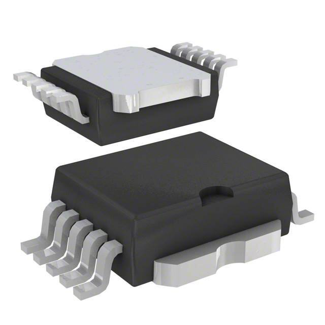
PowerSO-10
■
Primary coil voltage internally set
■
Coil current limit internally set
■
Logic level compatible input
Description
■
Driving current quasi proportional to collector
current
■
Double flag-on coil current
The VB027SP-E is a high voltage power
integrated circuit made using the
STMicroelectronics™ VIPower™ technology, with
vertical current flow power darlington and logic
level compatible driving circuit.
Built-in protection circuit for coil current limiting
and collector voltage clamping allows the device
to be used as smart, high voltage, high current
interface in advanced electronic ignition system.
Table 1.
Device summary
Order code
Package
PowerSO-10
May 2011
Doc ID 018828 Rev 1
Tube
Tape and reel
VB027SP-E
VB027SPTR-E
1/14
www.st.com
1
�Contents
VB027SP-E
Contents
1
Block diagram and pins description . . . . . . . . . . . . . . . . . . . . . . . . . . . . 5
2
Electrical specifications . . . . . . . . . . . . . . . . . . . . . . . . . . . . . . . . . . . . . . 6
3
4
5
2/14
2.1
Absolute maximum ratings . . . . . . . . . . . . . . . . . . . . . . . . . . . . . . . . . . . . . 6
2.2
Thermal data . . . . . . . . . . . . . . . . . . . . . . . . . . . . . . . . . . . . . . . . . . . . . . . 6
2.3
Electrical characteristics . . . . . . . . . . . . . . . . . . . . . . . . . . . . . . . . . . . . . . . 7
2.4
Electrical characteristics curves . . . . . . . . . . . . . . . . . . . . . . . . . . . . . . . . . 8
Application information . . . . . . . . . . . . . . . . . . . . . . . . . . . . . . . . . . . . . . 9
3.1
Principle of operation . . . . . . . . . . . . . . . . . . . . . . . . . . . . . . . . . . . . . . . . . 9
3.2
Thermal behaviour . . . . . . . . . . . . . . . . . . . . . . . . . . . . . . . . . . . . . . . . . . . 9
3.3
Overvoltage . . . . . . . . . . . . . . . . . . . . . . . . . . . . . . . . . . . . . . . . . . . . . . . 10
Package and packing information . . . . . . . . . . . . . . . . . . . . . . . . . . . . . 11
4.1
ECOPACK® . . . . . . . . . . . . . . . . . . . . . . . . . . . . . . . . . . . . . . . . . . . . . . . 11
4.2
PowerSO-10 mechanical data . . . . . . . . . . . . . . . . . . . . . . . . . . . . . . . . . 11
Revision history . . . . . . . . . . . . . . . . . . . . . . . . . . . . . . . . . . . . . . . . . . . 13
Doc ID 018828 Rev 1
�VB027SP-E
List of tables
List of tables
Table 1.
Table 2.
Table 3.
Table 4.
Table 5.
Table 6.
Table 7.
Device summary . . . . . . . . . . . . . . . . . . . . . . . . . . . . . . . . . . . . . . . . . . . . . . . . . . . . . . . . . . 1
Pin function . . . . . . . . . . . . . . . . . . . . . . . . . . . . . . . . . . . . . . . . . . . . . . . . . . . . . . . . . . . . . . 5
Absolute maximum ratings . . . . . . . . . . . . . . . . . . . . . . . . . . . . . . . . . . . . . . . . . . . . . . . . . . 6
Thermal data. . . . . . . . . . . . . . . . . . . . . . . . . . . . . . . . . . . . . . . . . . . . . . . . . . . . . . . . . . . . . 6
Electrical characteristics . . . . . . . . . . . . . . . . . . . . . . . . . . . . . . . . . . . . . . . . . . . . . . . . . . . . 7
PowerSO-10 mechanical data . . . . . . . . . . . . . . . . . . . . . . . . . . . . . . . . . . . . . . . . . . . . . . 11
Document revision history . . . . . . . . . . . . . . . . . . . . . . . . . . . . . . . . . . . . . . . . . . . . . . . . . 13
Doc ID 018828 Rev 1
3/14
�List of figures
VB027SP-E
List of figures
Figure 1.
Figure 2.
Figure 3.
Figure 4.
Figure 5.
Figure 6.
Figure 7.
Figure 8.
4/14
Block diagram . . . . . . . . . . . . . . . . . . . . . . . . . . . . . . . . . . . . . . . . . . . . . . . . . . . . . . . . . . . . 5
Configuration diagram (top view) . . . . . . . . . . . . . . . . . . . . . . . . . . . . . . . . . . . . . . . . . . . . . 5
Maximum Icl vs temperature . . . . . . . . . . . . . . . . . . . . . . . . . . . . . . . . . . . . . . . . . . . . . . . . . 8
IC(diag1) vs temperature . . . . . . . . . . . . . . . . . . . . . . . . . . . . . . . . . . . . . . . . . . . . . . . . . . . . . 8
IC(diag2) vs temperature . . . . . . . . . . . . . . . . . . . . . . . . . . . . . . . . . . . . . . . . . . . . . . . . . . . . . 8
Application circuit . . . . . . . . . . . . . . . . . . . . . . . . . . . . . . . . . . . . . . . . . . . . . . . . . . . . . . . . 10
Switching waveform . . . . . . . . . . . . . . . . . . . . . . . . . . . . . . . . . . . . . . . . . . . . . . . . . . . . . . 10
PowerSO-10 package dimensions . . . . . . . . . . . . . . . . . . . . . . . . . . . . . . . . . . . . . . . . . . . 12
Doc ID 018828 Rev 1
�VB027SP-E
1
Block diagram and pins description
Block diagram and pins description
Figure 1.
Block diagram
+9&
9G
,1387
'5,9(5
29(57(03�
� 3527(&7,21
48$6,�3523�
� %$6(�&855(17
�
)/$*��
�
56(16(
�
)/$*
)/$*��
5()(5(1&(
�
("1($'5�����
Figure 2.
Configuration diagram (top view)
�
�
�
�
�
*1'
9G
1�&��
,1387
',$*
�
�
*1'
*1'
*1'
*1'
*1'
�
��
�
��
+9&
("1($'5�����
Table 2.
Pin function
Pin number
Name
Function
1÷5
GND
Emitter power ground
6(1)
GND
Control ground
7
Vd
8
N.C.
9
INPUT
Logic input channel
10
DIAG
Diagnostic output signal
TAB
HVC
Primary coil output signal
Driving stage supply voltage
1. Pin 1÷5 = power GND, pin 6 = signal GND. Pin 6 must be connected to pins 1÷5 externally.
Doc ID 018828 Rev 1
5/14
�Electrical specifications
VB027SP-E
2
Electrical specifications
2.1
Absolute maximum ratings
Stressing the device above the rating listed in the Table 3: Absolute maximum ratings may
cause permanent damage to the device. These are stress ratings only and operation of the
device at these or any other conditions above those indicated in the operating sections of
this specification is not implied. Exposure to absolute maximum rating conditions for
extended periods may affect device reliability. Refer also to the STMicroelectronics SURE
program and other relevant quality documents.
Table 3.
Absolute maximum ratings
Symbol
Unit
Collector voltage
Internally limited
V
IC
Collector current
Internally limited
A
Vd
Driving stage supply voltage
7
V
Id
Driving circuitry supply current
200
mA
Input voltage
10
V
Junction operating temperature
-40 to 150
°C
Storage temperature
-55 to 150
°C
Value
Unit
Tj
Tstg
Thermal data
Table 4.
Symbol
6/14
Value
HVc
VIN
2.2
Parameter
Thermal data
Parameter
Rthj-case
Thermal resistance junction-case (MAX)
1.12
°C/W
Rthj-amb
Thermal resistance junction-ambient (MAX)
62.5
°C/W
Doc ID 018828 Rev 1
�VB027SP-E
Electrical specifications
2.3
Electrical characteristics
VCC = 13.5 V; Vd = 5 V; Tj = 25 °C; Rcoil = 510 mΩ; Lcoil = 7 mH unless otherwise specified.
Table 5.
Electrical characteristics
Symbol
Parameter
Test conditions
Min
Typ
Max
Unit
300
360
400
V
High voltage clamp
VIN = 0.4 V; -40 °C ≤ Tj ≤ 125 °C;
IC = 6 A
Vcg(sat)
Power stage saturation voltage
IC = 6 A; VIN = 4 V; Id = 80 mA
Vcg(sat)td
Power stage saturation voltage
derating in temperature
IC = 6 A; VIN = 4 V;
-40 °C ≤ Tj ≤ 125 °C; Id = 85 mA
2
V
Id(off)
Power-off supply current
VIN = 0.4 V
8
mA
Id(on)
Power-on supply current
VIN = 4 V; IC = 6 A;
-40 °C ≤ Tj ≤ 125 °C
130
mA
5.5
V
9
A
Vcl
Vd
Icl
Driving stage supply voltage
1.5
4.5
V(1)
Collector current limit
VIN = 4
Icl(td)
Collector current limit drift with
temperature
See Figure 3
VINH
High level input voltage
HVC < 2 V
4
5.5
V
VINL
Low level input voltage
IC < 2 mA; HVC = VCC
0
0.8
V
IINH
High level input current
VIN = 4 V
40
200
µA
Vd
V
0.5
V
VdiagH
High level diagnostic output voltage
REXT = 22 KΩ (See Figure 6)
VdiagL
Low level diagnostic output voltage
REXT = 22 KΩ (See Figure 6)
IC(diag1)
First threshold level collector current
IC(diag1)td
8
3.5
8.5
V
(2)
4.25
4.5
4.75
A
5.45
5.8
6.15
A
First threshold level collector current
See Figure 4
drift with temperature
IC(diag2)
Second threshold level collector
current
IC(diag2)td
Second threshold level collector
current drift with temperature
See Figure 5
td(off)
Turn-off delay time of output current
IC = 5.5 A
25
µs
tf(off)
Turn-off fall time of output current
IC = 5.5 A
8
µs
td(diag)
Delay time of diagnostic current
REXT = 22 KΩ (See Figure 6)
1
µs
tr(diag)
Turn-on rise time of diagnostic
current
REXT = 22 KΩ (See Figure 6)
1
µs
tf(diag)
Turn-off fall time of diagnostic
current
REXT = 22 KΩ (See Figure 6)
1
µs
1. The primary coil current value Icl must be measured 1 ms after desaturation of the power stage.
2. Vd - Vbe(on).
Doc ID 018828 Rev 1
7/14
�Electrical specifications
2.4
8/14
VB027SP-E
Electrical characteristics curves
Figure 3.
Maximum Icl vs temperature
Figure 5.
IC(diag2) vs temperature
Figure 4.
Doc ID 018828 Rev 1
IC(diag1) vs temperature
�VB027SP-E
Application information
3
Application information
3.1
Principle of operation
The VB027SP-E is mainly intended as high voltage power switch device driven by a logic
level input and interfaces directly to a high energy electronic ignition coil.
The input VIN of the VB027SP-E is fed from a low power signal generated by an external
controller that determines both dwell time and ignition point. During VIN high (≥ 4 V) the
VB027SP-E increases current in the coil to the desired, internally set current level.
When the collector current exceeds 4.5 A, the diagnostic signal is turned high and it remains
so, until the load current reaches 5.8 A (second threshold). At that value, the diagnostic
signal is turned low, and the µC forces the VIN to the low state. During the coil current
switch-off, the primary voltage HVC is clamped by a series of Zener diodes at an internally
set value Vcl, typically 360 V.
The collector current sensed through the Rsense, is limited thanks to the “Current limiter”
block that, as soon as the Icl level is reached, forces the darlington (using the “Driver” block)
to limit the current provided.
The transition from saturation to desaturation, coil current limiting phase, must have the
ability to accommodate an overvoltage. A maximum overshoot of 20 V is allowed. There can
be some short period of time in which the output pin (HVC) is pulled below ground by a
negative current due to leakage inductances and stray capacitances of the ignition coil. This
can cause parasitic glitches on the diagnostic output. VB027SP-E has a built-in protection
circuit that allows to lock the p-buried layer potential of the linear stage to the collector
power, when the last one is pulled underground.
3.2
Thermal behaviour
You can see in the block diagram of the VB027SP-E (see Figure 1) a box called
overtemperature protection. The purpose of this circuit is to shift the current level at which
the first diagnostic is activated down of about 1 A.
This information can be managed by the micro that can take the corrective action in order to
reduce the power dissipation. This block is not an effective protection but just an
overtemperature detection. The shift down of the first flag level cannot be present for
temperatures lower than 125 °C.
As an example of its behavior you can suppose a very simple motor management system in
which the micro does just a simple arithmetic calculation to decide when to switch-off the
device after the first flag threshold.
Example
IC(DIAG1) info after x ms (IC(DIAG1) = 2.5 A)
Iswitch-off info after kx ms.
As soon as the temperature rises over the overtemperature threshold, the first diagnostic is
shifted down to about 1.5 A and, in this example, the switch-off current is kx * 1.5 / 2.5.
Doc ID 018828 Rev 1
9/14
�Application information
3.3
VB027SP-E
Overvoltage
The VB027SP-E can withstand the following transients of the battery line:
-100 V / 2 ms (Ri = 10 Ω)
+100 V / 0.2 ms (Ri = 10 Ω)
+50 V / 400 ms (Ri = 4.2 Ω, with VIN = 3 V)
Figure 6.
Application circuit
Figure 7.
Switching waveform
9,1
�QG�7KUHVKROG
�VW�7KUHVKROG
,FO
',$*
("1($'5�����
10/14
Doc ID 018828 Rev 1
�VB027SP-E
Package and packing information
4
Package and packing information
4.1
ECOPACK®
In order to meet environmental requirements, ST offers these devices in different grades of
ECOPACK® packages, depending on their level of environmental compliance. ECOPACK®
specifications, grade definitions and product status are available at: www.st.com.
ECOPACK® is an ST trademark.
4.2
PowerSO-10 mechanical data
Table 6.
PowerSO-10 mechanical data
mm.
inch
Dim.
Min.
Typ
Max.
Min.
Typ.
Max.
A
3.35
3.65
0.132
0.144
A1
0.00
0.10
0.000
0.004
B
0.40
0.60
0.016
0.024
c
0.35
0.55
0.013
0.022
D
9.40
9.60
0.370
0.378
D1
7.40
7.60
0.291
0.300
E
9.30
9.50
0.366
0.374
E1
7.20
7.40
0.283
0.291
E2
7.20
7.60
0.283
0.299
E3
6.10
6.35
0.240
0.250
E4
5.90
6.10
0.232
0.240
e
1.27
0.050
F
1.25
1.35
0.049
0.053
H
13.80
14.40
0.543
0.567
h
0.50
0.002
Q
1.70
0.067
α
0°
8°
Doc ID 018828 Rev 1
11/14
�Package and packing information
Figure 8.
VB027SP-E
PowerSO-10 package dimensions
%
���� $ %
�
(�
�
%
H
����
(�
������
(�
������
(
(�
������
������
������
+
�
������
��
6($7,1*�
�3/$1(
'(7$,/��$�
$
&
0
4
K
'
������
'�
������
6($7,1*�
�3/$1(
$
)
$�
$�
/
'(7$,/��$�
A
("1($'5�����
12/14
Doc ID 018828 Rev 1
�VB027SP-E
5
Revision history
Revision history
Table 7.
Document revision history
Date
Revision
14-May-2011
1
Changes
Initial release.
Doc ID 018828 Rev 1
13/14
�VB027SP-E
Please Read Carefully:
Information in this document is provided solely in connection with ST products. STMicroelectronics NV and its subsidiaries (“ST”) reserve the
right to make changes, corrections, modifications or improvements, to this document, and the products and services described herein at any
time, without notice.
All ST products are sold pursuant to ST’s terms and conditions of sale.
Purchasers are solely responsible for the choice, selection and use of the ST products and services described herein, and ST assumes no
liability whatsoever relating to the choice, selection or use of the ST products and services described herein.
No license, express or implied, by estoppel or otherwise, to any intellectual property rights is granted under this document. If any part of this
document refers to any third party products or services it shall not be deemed a license grant by ST for the use of such third party products
or services, or any intellectual property contained therein or considered as a warranty covering the use in any manner whatsoever of such
third party products or services or any intellectual property contained therein.
UNLESS OTHERWISE SET FORTH IN ST’S TERMS AND CONDITIONS OF SALE ST DISCLAIMS ANY EXPRESS OR IMPLIED
WARRANTY WITH RESPECT TO THE USE AND/OR SALE OF ST PRODUCTS INCLUDING WITHOUT LIMITATION IMPLIED
WARRANTIES OF MERCHANTABILITY, FITNESS FOR A PARTICULAR PURPOSE (AND THEIR EQUIVALENTS UNDER THE LAWS
OF ANY JURISDICTION), OR INFRINGEMENT OF ANY PATENT, COPYRIGHT OR OTHER INTELLECTUAL PROPERTY RIGHT.
UNLESS EXPRESSLY APPROVED IN WRITING BY AN AUTHORIZED ST REPRESENTATIVE, ST PRODUCTS ARE NOT
RECOMMENDED, AUTHORIZED OR WARRANTED FOR USE IN MILITARY, AIR CRAFT, SPACE, LIFE SAVING, OR LIFE SUSTAINING
APPLICATIONS, NOR IN PRODUCTS OR SYSTEMS WHERE FAILURE OR MALFUNCTION MAY RESULT IN PERSONAL INJURY,
DEATH, OR SEVERE PROPERTY OR ENVIRONMENTAL DAMAGE. ST PRODUCTS WHICH ARE NOT SPECIFIED AS "AUTOMOTIVE
GRADE" MAY ONLY BE USED IN AUTOMOTIVE APPLICATIONS AT USER’S OWN RISK.
Resale of ST products with provisions different from the statements and/or technical features set forth in this document shall immediately void
any warranty granted by ST for the ST product or service described herein and shall not create or extend in any manner whatsoever, any
liability of ST.
ST and the ST logo are trademarks or registered trademarks of ST in various countries.
Information in this document supersedes and replaces all information previously supplied.
The ST logo is a registered trademark of STMicroelectronics. All other names are the property of their respective owners.
© 2011 STMicroelectronics - All rights reserved
STMicroelectronics group of companies
Australia - Belgium - Brazil - Canada - China - Czech Republic - Finland - France - Germany - Hong Kong - India - Israel - Italy - Japan Malaysia - Malta - Morocco - Philippines - Singapore - Spain - Sweden - Switzerland - United Kingdom - United States of America
www.st.com
14/14
Doc ID 018828 Rev 1
�