1. 物料型号:
- 型号为VB325SP。
2. 器件简介:
- VB325SP是一款使用STMicroelectronics VIPower™ M1-3技术制造的高压集成电路,具有垂直电流流通的达林顿结构和逻辑电平兼容的驱动电路。该器件集成了保护电路,用于线圈电流限制和集电极电压钳位,使其可以作为先进电子点火系统中的智能、高压、大电流接口。
3. 引脚分配:
- LGND (2-4脚):信号地、发射极电源地。
- E (6脚):使能引脚。
- VCC (7脚):逻辑供电电压。
- BD (8脚):达林顿基极。
- INPUT (9脚):逻辑输入通道(内部下拉)。
- HVC FLAG (10脚):诊断输出信号(开路发射极)主线圈输出驱动器(开路集电极)。
4. 参数特性:
- 工作电压:380V。
- 工作电流:10A。
- 驱动电流:150mA。
- 内部设定的主线圈电压和线圈电流限制。
- 逻辑电平兼容输入。
- 驱动电流与集电极电流成比例。
5. 功能详解:
- VB325SP主要用于高压功率开关设备,由逻辑电平输入驱动,直接接口至高能电子点火线圈。
- 当输入VIN为高电平时,VB325SP增加线圈中的电流至设定的内部电流水平,并在点火点保持恒定,直到VIN从高电平变为低电平。
- 在线圈电流关闭期间,主电压HVc被钳位在一个内部设定值vcl,通常为380V。
6. 应用信息:
- 该器件适用于高级电子点火系统,能够保护自身免受过热,并在输入信号保持高电平时平滑减少集电极电流,避免不期望的火花发生。
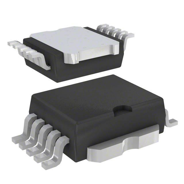
7. 封装信息:
- 封装为PowerSO-10™。