VB326SP
®
HIGH VOLTAGE IGNITION COIL DRIVER
POWER I.C.
TYPE
VB326SP
Vcl
360V
Icl
10A
ICC
150mA
PRIMARY COIL VOLTAGE INTERNALLY SET
COIL CURRENT LIMIT INTERNALLY SET
■ LOGIC LEVEL COMPATIBLE INPUT
■ DRIVING CURRENT QUASI PROPORTIONAL
TO COLLECTOR CURRENT
■
)
s
(
ct
■
■
SINGLE FLAG-ON COIL CURRENT
■
LOW VOLTAGE CLAMP THERMAL
SHUTDOWN
)
(s
e
t
e
ol
P
e
in advanced electronic ignition system. If the input
signal from the micro happens to remain high, the
device protects itself against over-heating by
forcing collector current to smooth decrease (low
voltage clamp feature) and no undesidered spark
occurs (see figure 4).
BD
VCC
t
e
l
o
bs
1
s
b
O
t
c
u
d
o
r
Pr
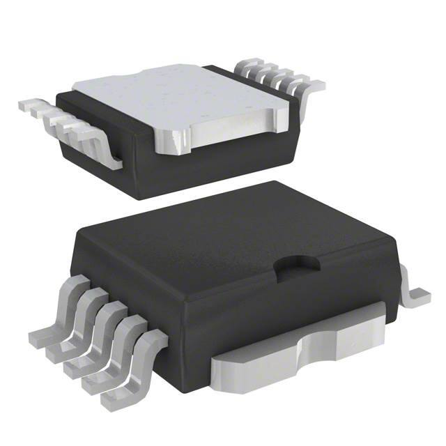
PowerSO-10™
DESCRIPTION
The VB326SP is a high voltage power integrated
circuit made using the STMicroelectronics
VIPower™ M1-3 technology, with vertical current
flow power darlington and logic level compatible
driving circuit. The enable pin allows to externally
block the switch when the input is on. Built-in
protection circuit for coil current limiting and
collector voltage clamping allows the device to be
used as smart, high voltage, high current interface
BLOCK DIAGRAM
u
d
o
10
HVC
VIN
DRIVER
O
QUASI PROP.
BASE CURRENT
RSENSE
LIMITER
DIAGNOSTIC
OUTPUT
VCC
VR
VF1
VLIM
-
THERMAL
PROTECTION
REFERENCE
VTH
SN
E
September 2013
LGND
DocID9672 Rev 6
GND
1/9
�VB326SP
ABSOLUTE MAXIMUM RATING
Symbol
HVc
IC
IC(gnd)
VCC
Is
Is(gnd)
VIN
IIN
fIN
VOUT(flag)
IOUT(flag)
Pmax
Es/b
VESD
VESD
VESD
IBD
VBD
Tj
Tstg
VE
IE
Parameter
Collector voltage (Internally limited)
Collector current (Internally limited)
DC current on Emitter Power
Driving stage supply voltage
Driving circuitry supply current
DC current on Ground pin
Input voltage
Maximum Input Current
Logic Input Frequency in Operative Mode
Output Voltage Primary Threshold Current Level
Flag Output Current
Power Dissipation (Tc=25°C)
Self Clamped Energy during Output Power Clamping (See figure 2)
ESD voltage (HVc pin)
ESD voltage (Enable pin)
ESD voltage (Other pins)
Input Darlington Base Current
Input Darlington Base Voltage
Operating Junction Temperature
Storage temperature Range
Maximum Enable Voltage
Maximum Enable Current
Unit
°C/W
°C/W
u
d
o
)
(s
s
b
O
t
c
u
Parameter
Thermal resistance junction-case
Thermal resistance junction-ambient
(MAX)
(MAX)
d
o
r
P
e
t
e
l
o
s
b
O
Value
1
51
)
s
(
ct
t
e
l
o
PIN FUNCTION
No
1-5
2-3-4
6
7
8
9
10
TAB
Unit
V
A
A
V
mA
A
V
mA
Hz
V
mA
W
mJ
KV
KV
KV
mA
V
°C
°C
V
µA
r
P
e
THERMAL DATA
Symbol
Rthj-case
Rthj-amb
Value
-0.3 to Vclamp
10
± 10.5
-0.3 to 7
± 200
±1
-0.3 to VCC + 0.3
100
DC to 150
-0.3 to VCC + 0.3
100
125
275
±4
+ 1.5 ; -2
±2
150
Internally limited
-40 to 150
-55 to 150
-0.3 to 5.5
± 150
Name
LGND
GND
E
VCC
BD
INPUT
FLAG
HVC
Function
Signal Ground
Emitter Power Ground
Enable (*)
Logic Supply Voltage
Base Darlington
Logic input channel (Internal Pull Down)
Diagnostic Output Signal (Open Emitter)
Primary Coil Output Driver (Open Collector)
(*) When grounded the Input is Enabled
CONNECTION DIAGRAM (TOP VIEW)
Pin 1 and Pin 5 must be externally connected to Pins 2÷4.
5
4
3
6
7
8
9
E
VCC
BD
INPUT
FLAG
2
10
1
TAB
HVC
2/9
LGND
GND
GND
GND
LGND
�VB326SP
ELECTRICAL CHARACTERISTICS (5.3V < Vbat < 24V; VCC=5V ± 10%; -40ºC < Tj < 125ºC; Rcoil=580mΩ;
Lcoil=3.75mH unless otherwise specified; See note 1)
Symbol
Vcl
Vlcl
Vce(sat)
ICC(stdby)
ICC
ICC(peak)
VCC
Icl
Ic(off)
Parameter
High Voltage Clamp
Low Voltage Clamp
Power Stage Saturation
Voltage
Stand-by Supply Current
Test Conditions
Icoil=6.5A
Icoil=6.5A; Tj=Tsd
IC=6A; VIN=4V
DC Logic Current
Peak DC Logic Current
during On Phase
DC Logic Voltage
IC=6.5A
Coil Current Limit
Turn-on time
tOFF
Turn-off time
VdiagH
VdiagL
IdiagTH
IdiagTD
Idiag
du
ro
t
e
l
o
Idiag(leak)
bs
VF
O
Tsd
VEH
VEL
1.5
2
V
11
mA
40
mA
)
s
(
ct
150
mA
5.5
V
11
A
5
mA
(*)
ºC
VIN=4V
VIN=0.8V
VIN=4V
150
let
o
s
b
Thermal shut-down
intervention
High Level Enable Voltage
Low Level Enable Voltage
ro
P
e
OUT=On
VCC=4.5V
VCC=5.5V
VCC
0.8
du
9
(See note 2)
IN=Off; VHVC=24V; VCC=5V; Tj=25ºC
O
)
REXT=22KΩ; CEXT=1nF (See note 3)
s
(
t
c
P
e
Unit
V
V
100
-40ºC < Tj < 125ºC
tON
VIN(hyst)
IINH
IINL
IINpd
Max
420
50
4.5
Es/b
VINH
VINL
Typ
360
40
IN=Off
Vb=16V; IC=6.5A; f=100Hz; Load = Coil;
VCC=5.5V
Output Off State Current
Thermal Temperature
Output Current Control
High Level Input Voltage
Low Level Input Voltage
Input Threshold Hysteresis
High Level Input Current
Low Level Input Current
Input Active Pull Down
High Level Flag Output
Voltage
Low Level Flag Output
Voltage
Coil Current Level Threshold
Coil Current Level Threshold
Drift
High Level Flag Output
Current
Leakage Current on Flag
Output
Antiparallel Diode Forward
Voltage
Single Pulse Avalanche
Energy
TIc_ctr
Min
320
30
4
-0.3
0.4
0
10
100
30
100
V
V
V
µA
µA
µA
VCC - 1
VCC
V
0.5
V
6.85
A
REXT=22KΩ; CEXT=1nF (See note 3)
Tj=25ºC
6.15
6.5
(See figure 1)
IC > IdiagTH; Vdiag=3V
0.5
mA
VIN=Low; VCC=5.5V
10
µA
IC= -1A
2
V
L=6mH; IC= 8A (See figure 2)
180
Rc=0.5Ω; Lc=3.75mH; Tj=25ºC;
Vbat=13V (See figure 6)
Rc=0.5Ω; Lc=3.75mH; IC=6.5A; Tj=25ºC;
Vbat=13V (See figure 6)
mJ
1
5
µs
15
25
µs
150
VIN=VINH; OUT=Off (See Note 4)
VOUT free to follow VIN
ºC
2
0.40
V
V
Note 1: parametric degratation are allowed with 5.3
很抱歉,暂时无法提供与“VB326SP”相匹配的价格&库存,您可以联系我们找货
免费人工找货