VBG15NB22T5SP-E
Ignition coil driver
Type
Vcl
Icl
VCEsat
VBG15NB22T5SP-E
250 V(1)
21 A(1)
1.7 V(1)
1. Typical value
)
s
(
ct
��
Features
■
ECOPACK®: lead free and RoHS compliant
■
Automotive Grade: compliance with AEC
guidelines
■
Low threshold voltage
■
Low on-voltage drop
■
Coil current limit internally set
■
High voltage clamping feature
■
ESD protection
■
Timing function externally set with
■
Soft switch-off
u
d
o
�
r
P
Description
e
t
e
l
o
s
b
-O
("1($'5�����
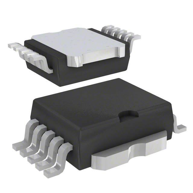
PowerSO-10
The VBG15NB22T5SP-E is an ignition coil driver
made by using the latest high voltage
Powermesh™ technology based on patented strip
lay-out.
(s)
The device is particularly suitable in high
performance car ignition, where coil current
limitation and precise voltage clamping are
required with no external component. ESD is an
additional inherent features.
t
c
u
d
o
r
P
e
t
e
l
o
s
b
O
Table 1.
Device summary
Order code
Package
PowerSO-10
May 2011
Tube
Tape and reel
VBG15NB22T5SP-E
VBG15NB22T5TR-E
Doc ID 018832 Rev 1
1/16
www.st.com
1
�Contents
VBG15NB22T5SP-E
Contents
1
Block diagram and pins connection . . . . . . . . . . . . . . . . . . . . . . . . . . . . 5
2
Electrical specifications . . . . . . . . . . . . . . . . . . . . . . . . . . . . . . . . . . . . . . 6
3
2.1
Absolute maximum ratings . . . . . . . . . . . . . . . . . . . . . . . . . . . . . . . . . . . . . 6
2.2
Thermal data . . . . . . . . . . . . . . . . . . . . . . . . . . . . . . . . . . . . . . . . . . . . . . . 6
2.3
Functional characteristics . . . . . . . . . . . . . . . . . . . . . . . . . . . . . . . . . . . . . . 6
2.4
Electrical characteristics . . . . . . . . . . . . . . . . . . . . . . . . . . . . . . . . . . . . . . . 7
2.5
Timer block function . . . . . . . . . . . . . . . . . . . . . . . . . . . . . . . . . . . . . . . . . 10
)
s
(
ct
u
d
o
4
Package and packing information . . . . . . . . . . . . . . . . . . . . . . . . . . . . . 12
r
P
e
3.1
ECOPACK® . . . . . . . . . . . . . . . . . . . . . . . . . . . . . . . . . . . . . . . . . . . . . . . 12
3.2
PowerSO-10 mechanical data . . . . . . . . . . . . . . . . . . . . . . . . . . . . . . . . . 12
3.3
PowerSO-10 packing information . . . . . . . . . . . . . . . . . . . . . . . . . . . . . . . 14
t
e
l
o
s
b
O
Revision history . . . . . . . . . . . . . . . . . . . . . . . . . . . . . . . . . . . . . . . . . . . 15
)
(s
t
c
u
d
o
r
P
e
t
e
l
o
s
b
O
2/16
Doc ID 018832 Rev 1
�VBG15NB22T5SP-E
List of tables
List of tables
Table 1.
Table 2.
Table 3.
Table 4.
Table 5.
Table 6.
Table 7.
Table 8.
Table 9.
Table 10.
Device summary . . . . . . . . . . . . . . . . . . . . . . . . . . . . . . . . . . . . . . . . . . . . . . . . . . . . . . . . . . 1
Absolute maximum ratings . . . . . . . . . . . . . . . . . . . . . . . . . . . . . . . . . . . . . . . . . . . . . . . . . . 6
Thermal data. . . . . . . . . . . . . . . . . . . . . . . . . . . . . . . . . . . . . . . . . . . . . . . . . . . . . . . . . . . . . 6
Functional characteristics . . . . . . . . . . . . . . . . . . . . . . . . . . . . . . . . . . . . . . . . . . . . . . . . . . . 6
Electrical characteristics . . . . . . . . . . . . . . . . . . . . . . . . . . . . . . . . . . . . . . . . . . . . . . . . . . . . 7
Electrical transient requirements on VCC pin (part 1/3). . . . . . . . . . . . . . . . . . . . . . . . . . . . . 9
Electrical transient requirements on VCC pin (part 2/3). . . . . . . . . . . . . . . . . . . . . . . . . . . . . 9
Electrical transient requirements on VCC pin (part 3/3). . . . . . . . . . . . . . . . . . . . . . . . . . . . 10
PowerSO-10 mechanical data . . . . . . . . . . . . . . . . . . . . . . . . . . . . . . . . . . . . . . . . . . . . . . 13
Document revision history . . . . . . . . . . . . . . . . . . . . . . . . . . . . . . . . . . . . . . . . . . . . . . . . . 15
)
s
(
ct
u
d
o
r
P
e
t
e
l
o
)
(s
s
b
O
t
c
u
d
o
r
P
e
t
e
l
o
s
b
O
Doc ID 018832 Rev 1
3/16
�List of figures
VBG15NB22T5SP-E
List of figures
Figure 1.
Figure 2.
Figure 3.
Figure 4.
Figure 5.
Figure 6.
Figure 7.
Figure 8.
Figure 9.
Figure 10.
Figure 11.
Figure 12.
Block diagram . . . . . . . . . . . . . . . . . . . . . . . . . . . . . . . . . . . . . . . . . . . . . . . . . . . . . . . . . . . . 5
Connection diagram (top view) . . . . . . . . . . . . . . . . . . . . . . . . . . . . . . . . . . . . . . . . . . . . . . . 5
Typical application circuit . . . . . . . . . . . . . . . . . . . . . . . . . . . . . . . . . . . . . . . . . . . . . . . . . . . 8
tstill definition . . . . . . . . . . . . . . . . . . . . . . . . . . . . . . . . . . . . . . . . . . . . . . . . . . . . . . . . . . . . . 8
tstill specification . . . . . . . . . . . . . . . . . . . . . . . . . . . . . . . . . . . . . . . . . . . . . . . . . . . . . . . . . . 9
ISO pulses test circuit . . . . . . . . . . . . . . . . . . . . . . . . . . . . . . . . . . . . . . . . . . . . . . . . . . . . . 10
Typical waveforms . . . . . . . . . . . . . . . . . . . . . . . . . . . . . . . . . . . . . . . . . . . . . . . . . . . . . . . 11
Timer block schematic . . . . . . . . . . . . . . . . . . . . . . . . . . . . . . . . . . . . . . . . . . . . . . . . . . . . 11
PowerSO-10 package dimensions . . . . . . . . . . . . . . . . . . . . . . . . . . . . . . . . . . . . . . . . . . . 12
PowerSO-10 suggested PAD layout. . . . . . . . . . . . . . . . . . . . . . . . . . . . . . . . . . . . . . . . . . 14
PowerSO-10 tube shipment (no suffix) . . . . . . . . . . . . . . . . . . . . . . . . . . . . . . . . . . . . . . . . 14
PowerSO-10 tape and reel shipment (suffix “13TR”) . . . . . . . . . . . . . . . . . . . . . . . . . . . . . 14
)
s
(
ct
u
d
o
r
P
e
t
e
l
o
)
(s
s
b
O
t
c
u
d
o
r
P
e
t
e
l
o
s
b
O
4/16
Doc ID 018832 Rev 1
�VBG15NB22T5SP-E
1
Block diagram and pins connection
Block diagram and pins connection
Figure 1.
Block diagram
6##
(6#
)3/
02/4%#4)/.
/6%26/,4!'%�
02/4%#4)/.
).054
4)-%2
2/
2%&%2%.#%
r
P
e
t
e
l
o
)
(s
r
P
e
).054
6##
#STILL
.�#�
.�#�
t
c
u
23%.3%
'2/5.$
'!0'#&4�����
s
b
O
Connection diagram (top view)
od
u
d
o
#522%.4
,)-)4%2
/6%24%-0�
02/4%#4)/.
#STILL
Figure 2.
)
s
(
ct
$2)6%2
�
�
�
�
�
�
�
'2/5.$
'2/5.$
'2/5.$
'2/5.$
'2/5.$
�
��
�
��
(6#
t
e
l
o
'!0'#&4�����
s
b
O
Doc ID 018832 Rev 1
5/16
�Electrical specifications
VBG15NB22T5SP-E
2
Electrical specifications
2.1
Absolute maximum ratings
Stressing the device above the rating listed in the Table 2: Absolute maximum ratings may
cause permanent damage to the device. These are stress ratings only and operation of the
device at these or any other conditions above those indicated in the operating sections of
this specification is not implied. Exposure to absolute maximum rating conditions for
extended periods may affect device reliability. Refer also to the STMicroelectronics SURE
program and other relevant quality documents.
Table 2.
Absolute maximum ratings
Symbol
VCES
Input voltage
VCC
Maximum supply voltage
Ptot
VESD
Tj
Tstg
Value
Unit
Clamped
u
d
o
V
-16 to 18
V
24
V
Internally limited
A
125
W
2000
V
-40 to 175
°C
-40 to 175
°C
40
V
40
V
Collector-Emitter voltage
VIN
IC
)
s
(
ct
Parameter
Collector current (continuous)
e
t
e
ol
Total dissipation at Tcase = 25 °C
Pr
Electrostatic discharge (R = 1.5 KΩ; C = 100 pF)
s
b
O
Operating junction temperature
Storage temperature
)
(s
VCC-GND Pulsed VCC to ground voltage (tp = 50 µs; VCC - GND)
VCC-HVc
2.2
d
o
r
Thermal data
P
e
Table 3.
t
e
l
o
t
c
u
Pulsed VCC to HVC voltage (tp = 50 µs; VCC - HVC)
Thermal data
Symbol
s
b
O
2.3
Value
Unit
Rthj-case
Thermal resistance junction-case (MAX)
1
°C/W
Rthj-amb
Thermal resistance junction-ambient (MAX)
50
°C/W
Functional characteristics
Table 4.
Symbol
6/16
Parameter
Functional characteristics
Parameter
Eas
Avalanche energy
VCC
DC supply voltage
Test conditions
Min
Tj = 150 °C
5.2
Doc ID 018832 Rev 1
Typ
Max
Unit
250
mJ
24
V
�VBG15NB22T5SP-E
2.4
Electrical specifications
Electrical characteristics
Tj = 25 °C; VCC = 14 V; L = 1 mH; RL = 100 mΩ unless otherwise specified.
Table 5.
Electrical characteristics
Symbol
Parameter
Test conditions
Min Typ Max
Unit
OFF
Vcl
Clamp voltage
IC = 15 A; VIN = 0 V;
Tj = -40 to 150 °C
IS
Supply current (VCC)
Vbat = 16 V; VIN = 0 V;
Tj = -40 to 150 °C (see Figure 3)
ICES
Collector-emitter leakage
current
225 250
VCE(sat)
Collector-emitter saturation
voltage
VIN = 3 V; IC = 15 A;
-40 °C < Tj < 150 °C
VCE(sat)
Collector-emitter saturation
voltage
VIN = 3V; IC = 10A;
-40 °C < Tj < 150 °C; Vbat = 6 V
(See figure 1)
let
o
s
b
-O
IIN = 5 mA; -40 °C < Tj < 150 °C
VIN
t
c
u
VIN(on)
Input voltage on
VIN(off)
Input voltage off
od
r
P
e
Dynamic
COES
t
e
l
o
(s)
Input voltage
u
d
o
r
P
e
ON(1)
mA
40
µA
200
µA
2.5
V
2.2
V
V
4.2
3
1.5
VCE = 25 V; f = 1 MHz
V
V
-40 °C < Tj < 150 °C
Output capacitance
10
3
IIN = 10 mA;
-40 °C < Tj < 150 °C
-40 °C < Tj < 150 °C
V
)
s
(
ct
VCE = 175 V; VIN = 0 V;
VCC = 0 V
VCE = 175 V; VIN = 0 V;
Tj = 150 °C; VCC = 0 V
275
V
125
pF
2.7
µs
180
µJ
Switching on
O
bs
td(on)
Turn-on delay time
Eon
Turn-on switching losses
From input signal to VCE(sat) = 3 V
Switching off
td(off)
Off voltage delay time
Eoff(2)
Turn-off switching losses
td(off)
Off voltage delay time
Eoff(2)
tr
IC = 15 A; VCE = 100 V;
Tcase = 25 °C
5
5
Turn-off switching losses
IC = 15A; VCE = 100 V:
Tcase = 125 °C
Voltage rise time
From VCE = 50 V to VCE = 150 V
15
7.5
µs
mJ
15
10
µs
mJ
3
µs
25
A
Protection
Icl
Coil current limit
VIN = 3 V; 10 V < VCC < 24 V
Doc ID 018832 Rev 1
17
7/16
�Electrical specifications
Table 5.
VBG15NB22T5SP-E
Electrical characteristics (continued)
Symbol
Parameter
Test conditions
Min Typ Max
Unit
Timing function
(3)
tstill
dIc/dt
Capacitor charging time
Cstill = 100 nF; 100 < Tj < 175 °C
Turn-off current slope
Cstill = 100 nF
(see Figure 3,
Figure 4,
Figure 5)
0.1
2
ms
A/ms
1. Pulsed: pulse duration = 300 µs; duty cycle = 1.5 %
2. Losses include also the tail (Jedec Standardization)
3. The function is guaranteed by design to be operative in full temperature range.
Figure 3.
)
s
(
ct
Typical application circuit
u
d
o
9EDW
9&&
)-
s
b
O
s
b
O
9%*��1%��7�63
&VWLOO
e
t
e
ol
t
e
l
o
+9&
,1387
Figure 4.
r
P
e
+�9� 'LRGH
*5281'
s
(
t
c
("1($'5�����
u
d
o
tstill definition
Pr
,F
,FO
G ,� G W
W
9F
9UHI
WVWLOO
W
("1($'5�����
8/16
Doc ID 018832 Rev 1
�VBG15NB22T5SP-E
Figure 5.
Electrical specifications
tstill specification
TSTILL �MSEC
��
��
��
��
��
��
��
��
��
)
s
(
ct
�
�
�
�
�
��
��
��
��
6BATT �6
t
e
l
o
Test levels
ISO T/R 7637/1
Test pulse
III
IV
Delay and
impedance
-75V
-100V
2ms, 10Ω
50V
75V
100V
0.2ms, 10Ω
-50V
-100V
-150V
0.1µs, 50Ω
25V
50V
75V
100V
0.1µs, 50Ω
-4V
-5V
-6V
-7V
100ms, 0.01Ω
26.5V
46.5V
66.5V
86.5V
400ms, 2Ω
I
II
1
-25V
-50V
2
25V
3a
-25V
)-
s
(
t
c
du
3b
ro
4
P
e
t
e
l
o
r
P
e
Electrical transient requirements on VCC pin(1) (part 1/3)
Table 6.
5
u
d
o
��
'!0'#&4�����
s
b
O
1. See Figure 6, Vbat = 12 V.
O
bs
Table 7.
Electrical transient requirements on VCC pin (part 2/3)
ISO T/R 7637/1
Test pulse
Test level results
I
II
III
IV
Delay and
impedance
1
C
C
E
E
2ms, 10Ω
2
C
E
E
E
0.2ms, 10Ω
3a
C
C
C
C
0.1µs, 50Ω
3b
C
C
C
C
0.1µs, 50Ω
4
C
E
C
C
100ms, 0.01Ω
5
C
C
E
E
400ms, 2Ω
Doc ID 018832 Rev 1
9/16
�Electrical specifications
Table 8.
VBG15NB22T5SP-E
Electrical transient requirements on VCC pin (part 3/3)
Class
Contents
C
All functions of the device performed as designed after exposure to disturbance.
E
One or more functions of the device did not perform as designed after exposure to
disturbance and cannot be returned to proper operation without replacing the device.
Figure 6.
ISO pulses test circuit
9EDW
)
s
(
ct
/ �P+
9&&
,1387
r
P
e
9%*��1%��7�63
&VWLOO
)
s
Timer block function
(
t
c
u
d
o
r
P
e
t
e
ol
2.5
u
d
o
+9&
t
e
l
o
*5281'
s
b
O
("1($'5�����
The VBG15NB22T5SP-E has a timer block built-in (see Figure 8), in order to have a soft
switch-off of the device. When an input signal is provided to the device (see Figure 7, case
a), the external capacitor starts its charging through the Switch1 (with a slope depending on
VCC) and goes on until it reaches the Vref voltage (see Figure 7, case b). As soon as it
happens, the voltage comparator gives an enable signal (see Figure 7, case c) that
develops different functions:
s
b
O
10/16
●
It opens Switch1 and closes Switch2, so that the external capacitor discharges.
●
It provides power to the transconductance inverting amplifier, the input of which is
theexternal capacitor voltage.
It means that while VC decreases, Itimer (see Figure 7, case d) increases proportionally. The
increasing drop voltage on RO, due to Itimer, has to be compensated by a reducing drop
voltage on RSENSE, so to maintain the A input voltage equal to the B one. Since the RSENSE
drop depends on the coil current, it means that a soft decreasing of it occurs (see Figure 7,
case e).
Doc ID 018832 Rev 1
�VBG15NB22T5SP-E
Figure 7.
Electrical specifications
Typical waveforms
'RAPHICA
6).
6REF
6BAT��6
6BAT���6
'RAPHICB
6C
6BAT��6
'RAPHICC
6BAT���6
%.
'RAPHICD
)TIMER
6BAT���6
6BAT��6
'RAPHICE
Figure 8.
6BAT��6
e
t
e
ol
s
b
O
u
d
o
r
P
e
Timer block schematic
t
e
l
o
)-
t(s
c
u
d
o
r
P
s
b
O
,F
75$16&21'8&7$1&(
,19(57,1*
$03/,),(5
VSDUN
,WLPHU
,*%7
52
6ZLWFK�
6ZLWFK�
92/7$*(
&203$5$725
'!0'#&4�����
&2,/
9UHI
,&&
9,1
)C
6BAT���6
9&&
&VWLOO
)
s
(
ct
(1
'LVFKDUJH
$
56(16( %
&855(17
/,0,7(5
5HIHUHQFH
,ULI
7,0(5
("1($'5�����
Doc ID 018832 Rev 1
11/16
�Package and packing information
VBG15NB22T5SP-E
3
Package and packing information
3.1
ECOPACK®
In order to meet environmental requirements, ST offers these devices in different grades of
ECOPACK® packages, depending on their level of environmental compliance. ECOPACK®
specifications, grade definitions and product status are available at: www.st.com.
ECOPACK® is an ST trademark.
3.2
PowerSO-10 mechanical data
Figure 9.
)
s
(
ct
PowerSO-10 package dimensions
u
d
o
%
r
P
e
���� $ %
��
+
(
t
e
l
o
(
(�
�
H
t
c
u
����
d
o
r
K
P
e
)
(s
%
s
b
O
'(7$,/��$�
6($7,1*
�3/$1(
$
&
'
������
'�
������
6($7,1*
�3/$1(
$
t
e
l
o
)
$�
$�
s
b
O
(�
/
'(7$,/��$�
D
("1($'5�����
12/16
Doc ID 018832 Rev 1
�VBG15NB22T5SP-E
Table 9.
Package and packing information
PowerSO-10 mechanical data
mm.
inch
Dim.
Min.
Typ
Typ.
Max.
3.35
3.65
0.132
0.144
A(1)
3.4
3.6
0.134
0.142
A1
0.00
0.10
0.000
0.004
B
0.40
0.60
0.016
0.024
(1)
0.37
0.53
0.014
0.021
C
0.35
0.55
0.013
0.022
C(1)
0.23
0.32
0.009
D
9.40
9.60
0.370
D1
7.40
7.60
0.291
E
9.30
9.50
0.366
E2
7.20
7.60
0.283
7.30
7.50
5.90
(1)
E2
E4
(1)
F
1.25
(1)
1.20
F
H
13.80
H(1)
u
d
o
h
L
)
s
(
ct
13.85
Pr
u
d
o
Pr
0.378
0.300
0.374
0.299
o
s
b
0.232
0.240
0.232
0.248
1.35
0.049
0.053
1.40
0.047
0.055
14.40
0.543
0.567
14.35
0.545
0.565
6.30
1.27
0.0126
0.295
6.10
e
e
t
e
l
)
s
(
ct
0.287
5.90
E4
-O
0.050
0.50
0.002
1.20
1.80
0.047
0.070
0.80
1.10
0.031
0.043
α
0°
8°
0°
8°
(1)
2°
8°
2°
8°
e
t
e
l
(1)
L
b
O
Min.
A
B
so
Max.
α
1. Muar only POA P013P.
Doc ID 018832 Rev 1
13/16
�Package and packing information
3.3
VBG15NB22T5SP-E
PowerSO-10 packing information
Figure 10. PowerSO-10
suggested PAD
layout
Figure 11.
�����������
PowerSO-10 tube shipment (no suffix)
#!3!",!.#!
"
���������
-5!2
#
����
#
!
!
"
�����������
�
��
�
�
�
���
����������
!LLDIMENSIONSAREINMM�
�
�
�
�
����
#ASABLANCA
�
)
s
(
ct
"ASE1�TY "ULK1�TY 4U BELENGTH� ��� !
" #����
��
����
���
���� ����
���
-UAR
��
����
���
��� ����
du
("1($'5�����
'!0'#&4�����
o
r
P
Figure 12. PowerSO-10 tape and reel shipment (suffix “13TR”)
e
t
e
l
���
5((/�',0(16,216
o
s
b
O
)
s
(
t
c
du
o
r
P
%DVH�4�W\
%XON�4�W\
$��PD[�
%��PLQ�
&�������
)
*�����������
1��PLQ�
7��PD[�
���
���
���
���
��
����
����
��
����
$OO�GLPHQVLRQV�DUH�LQ�PP�
7$3(�',0(16,216
$FFRUGLQJ�WR�(OHFWURQLF�,QGXVWULHV�$VVRFLDWLRQ
�(,$��6WDQGDUG�����UHY��$��)HE�����
e
t
e
l
o
s
b
O
7DSH�ZLGWK�
7DSH�+ROH�6SDFLQJ
&RPSRQHQW�6SDFLQJ
+ROH�'LDPHWHU
+ROH�'LDPHWHU
+ROH�3RVLWLRQ
&RPSDUWPHQW�'HSWK
+ROH�6SDFLQJ
:
3��������
3
'����������
'���PLQ�
)��������
.��PD[�
3��������
$OO�GLPHQVLRQV�DUH�LQ�PP�
��
�
��
���
���
����
���
�
(QG
6WDUW
7RS
1R�FRPSRQHQWV
&RPSRQHQWV
1R�FRPSRQHQWV
FRYHU
WDSH
���PP�PLQ
(PSW\�FRPSRQHQWV�SRFNHWV
VDOHG�ZLWK�FRYHU�WDSH�
���PP�PLQ
8VHU�GLUHFWLRQ�RI�IHHG
("1($'5�����
14/16
Doc ID 018832 Rev 1
�VBG15NB22T5SP-E
4
Revision history
Revision history
Table 10.
Document revision history
Date
Revision
20-May-2011
1
Changes
Initial release.
)
s
(
ct
u
d
o
r
P
e
t
e
l
o
)
(s
s
b
O
t
c
u
d
o
r
P
e
t
e
l
o
s
b
O
Doc ID 018832 Rev 1
15/16
�VBG15NB22T5SP-E
)
s
(
ct
Please Read Carefully:
u
d
o
Information in this document is provided solely in connection with ST products. STMicroelectronics NV and its subsidiaries (“ST”) reserve the
right to make changes, corrections, modifications or improvements, to this document, and the products and services described herein at any
time, without notice.
r
P
e
All ST products are sold pursuant to ST’s terms and conditions of sale.
Purchasers are solely responsible for the choice, selection and use of the ST products and services described herein, and ST assumes no
liability whatsoever relating to the choice, selection or use of the ST products and services described herein.
t
e
l
o
No license, express or implied, by estoppel or otherwise, to any intellectual property rights is granted under this document. If any part of this
document refers to any third party products or services it shall not be deemed a license grant by ST for the use of such third party products
or services, or any intellectual property contained therein or considered as a warranty covering the use in any manner whatsoever of such
third party products or services or any intellectual property contained therein.
)
(s
s
b
O
UNLESS OTHERWISE SET FORTH IN ST’S TERMS AND CONDITIONS OF SALE ST DISCLAIMS ANY EXPRESS OR IMPLIED
WARRANTY WITH RESPECT TO THE USE AND/OR SALE OF ST PRODUCTS INCLUDING WITHOUT LIMITATION IMPLIED
WARRANTIES OF MERCHANTABILITY, FITNESS FOR A PARTICULAR PURPOSE (AND THEIR EQUIVALENTS UNDER THE LAWS
OF ANY JURISDICTION), OR INFRINGEMENT OF ANY PATENT, COPYRIGHT OR OTHER INTELLECTUAL PROPERTY RIGHT.
t
c
u
UNLESS EXPRESSLY APPROVED IN WRITING BY AN AUTHORIZED ST REPRESENTATIVE, ST PRODUCTS ARE NOT
RECOMMENDED, AUTHORIZED OR WARRANTED FOR USE IN MILITARY, AIR CRAFT, SPACE, LIFE SAVING, OR LIFE SUSTAINING
APPLICATIONS, NOR IN PRODUCTS OR SYSTEMS WHERE FAILURE OR MALFUNCTION MAY RESULT IN PERSONAL INJURY,
DEATH, OR SEVERE PROPERTY OR ENVIRONMENTAL DAMAGE. ST PRODUCTS WHICH ARE NOT SPECIFIED AS "AUTOMOTIVE
GRADE" MAY ONLY BE USED IN AUTOMOTIVE APPLICATIONS AT USER’S OWN RISK.
d
o
r
P
e
t
e
l
o
Resale of ST products with provisions different from the statements and/or technical features set forth in this document shall immediately void
any warranty granted by ST for the ST product or service described herein and shall not create or extend in any manner whatsoever, any
liability of ST.
s
b
O
ST and the ST logo are trademarks or registered trademarks of ST in various countries.
Information in this document supersedes and replaces all information previously supplied.
The ST logo is a registered trademark of STMicroelectronics. All other names are the property of their respective owners.
© 2011 STMicroelectronics - All rights reserved
STMicroelectronics group of companies
Australia - Belgium - Brazil - Canada - China - Czech Republic - Finland - France - Germany - Hong Kong - India - Israel - Italy - Japan Malaysia - Malta - Morocco - Philippines - Singapore - Spain - Sweden - Switzerland - United Kingdom - United States of America
www.st.com
16/16
Doc ID 018832 Rev 1
�