VIPer11
Energy saving offline high voltage converter
Datasheet - production data
Applications
Low power SMPS for home appliances, home
automation, industrial, consumer, lighting
Low power adapters
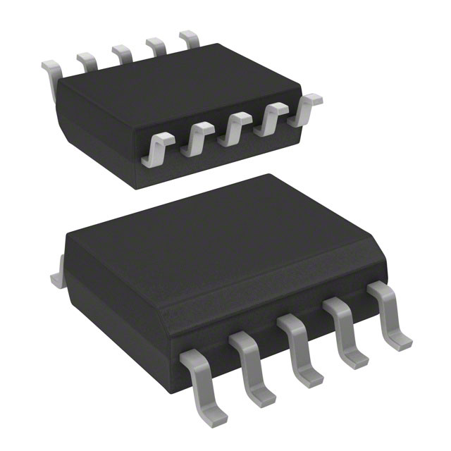
SSOP10
Description
Features
800 V avalanche-rugged power MOSFET
allowing ultra wide VAC input range to be
covered
Embedded HV startup and sense-FET
Current mode PWM controller
Drain current limit protection
– 370 mA (VIPER113)
– 480 mA (VIPER114)
– 590 mA (VIPER115)
Wide supply voltage range: 4.5 V to 30 V
Minimized system input power consumption:
– Less than 10 mW at 230 VAC in no-load
condition
– Less than 400 mW at 230 VAC with 250
mW load
The device is a high voltage converter smartly
integrating an 800 V avalanche-rugged power
MOSFET with PWM current mode control. The
power MOSFET with 800 V breakdown voltage
allows the extended input voltage range to be
applied, as well as the size of the DRAIN snubber
circuit to be reduced. This IC meets the most
stringent energy-saving standards as it has very
low consumption and operates in pulse frequency
modulation under light load. The design of
flyback, buck and buck boost converters is
supported. The integrated HV startup, senseFET, error amplifier and oscillator with jitter allow
a complete application to be designed with the
minimum number of components.
Figure 1. Basic application schematic
Jittered switching frequency reduces the EMI
filter cost:
– 30 kHz ± 7% (type X)
– 60 kHz ± 7% (type L)
– 120kHz ± 7%(type H)
Embedded E/A with 1.2 V reference
Protections with automatic restart:
overload/short-circuit (OLP), line or output
OVP, max. duty cycle counter, VCC clamp
Pulse-skip protection to prevent flux- runaway
Embedded thermal shutdown
".������
Built-in soft-start for improved system reliability
April 2020
This is information on a product in full production.
DS11873 Rev 5
1/37
www.st.com
�Contents
VIPer11
Contents
1
Pin setting . . . . . . . . . . . . . . . . . . . . . . . . . . . . . . . . . . . . . . . . . . . . . . . . . 4
2
Electrical and thermal ratings . . . . . . . . . . . . . . . . . . . . . . . . . . . . . . . . . 6
3
Electrical characteristics . . . . . . . . . . . . . . . . . . . . . . . . . . . . . . . . . . . . . 8
4
Typical electrical characteristics . . . . . . . . . . . . . . . . . . . . . . . . . . . . . . 12
5
General description . . . . . . . . . . . . . . . . . . . . . . . . . . . . . . . . . . . . . . . . . 16
6
7
5.1
Block diagram . . . . . . . . . . . . . . . . . . . . . . . . . . . . . . . . . . . . . . . . . . . . . . 16
5.2
Typical power capability . . . . . . . . . . . . . . . . . . . . . . . . . . . . . . . . . . . . . . 16
5.3
Primary MOSFET . . . . . . . . . . . . . . . . . . . . . . . . . . . . . . . . . . . . . . . . . . . 17
5.4
High voltage startup . . . . . . . . . . . . . . . . . . . . . . . . . . . . . . . . . . . . . . . . . 17
5.5
Soft-start . . . . . . . . . . . . . . . . . . . . . . . . . . . . . . . . . . . . . . . . . . . . . . . . . . 19
5.6
Oscillator . . . . . . . . . . . . . . . . . . . . . . . . . . . . . . . . . . . . . . . . . . . . . . . . . 19
5.7
Pulse-skipping . . . . . . . . . . . . . . . . . . . . . . . . . . . . . . . . . . . . . . . . . . . . . 20
5.8
Direct feedback . . . . . . . . . . . . . . . . . . . . . . . . . . . . . . . . . . . . . . . . . . . . 21
5.9
Secondary feedback . . . . . . . . . . . . . . . . . . . . . . . . . . . . . . . . . . . . . . . . . 21
5.10
Pulse frequency modulation . . . . . . . . . . . . . . . . . . . . . . . . . . . . . . . . . . . 21
5.11
Overload protection . . . . . . . . . . . . . . . . . . . . . . . . . . . . . . . . . . . . . . . . . 22
5.12
Max. duty cycle counter protection . . . . . . . . . . . . . . . . . . . . . . . . . . . . . . 23
5.13
VCC clamp protection . . . . . . . . . . . . . . . . . . . . . . . . . . . . . . . . . . . . . . . 23
5.14
Disable function . . . . . . . . . . . . . . . . . . . . . . . . . . . . . . . . . . . . . . . . . . . . 24
5.15
Thermal shutdown . . . . . . . . . . . . . . . . . . . . . . . . . . . . . . . . . . . . . . . . . . 26
5.16
Auto-restart . . . . . . . . . . . . . . . . . . . . . . . . . . . . . . . . . . . . . . . . . . . . . . . . 27
Application information . . . . . . . . . . . . . . . . . . . . . . . . . . . . . . . . . . . . . 28
6.1
Typical schematics . . . . . . . . . . . . . . . . . . . . . . . . . . . . . . . . . . . . . . . . . . 28
6.2
Energy saving performance . . . . . . . . . . . . . . . . . . . . . . . . . . . . . . . . . . . 31
6.3
Layout guidelines and design recommendations . . . . . . . . . . . . . . . . . . . 32
Package information . . . . . . . . . . . . . . . . . . . . . . . . . . . . . . . . . . . . . . . . 34
7.1
2/37
SSOP10 package information . . . . . . . . . . . . . . . . . . . . . . . . . . . . . . . . . 34
DS11873 Rev 5
�VIPer11
Contents
8
Ordering information . . . . . . . . . . . . . . . . . . . . . . . . . . . . . . . . . . . . . . . 36
9
Revision history . . . . . . . . . . . . . . . . . . . . . . . . . . . . . . . . . . . . . . . . . . . 36
DS11873 Rev 5
3/37
37
�Pin setting
1
VIPer11
Pin setting
Figure 2. Connection diagram
Table 1. Pin description
SSOP10
1
2
3
4
4/37
Name
Function
GND
Ground and MOSFET source. Connection of source of the internal MOSFET
and the return of the bias current of the device. All groundings of bias
components must be tied to a trace going to this pin and kept separate from the
pulsed current return.
VCC
Controller supply. An external storage capacitor has to be connected across
this pin and GND. The pin, internally connected to the high voltage current
source, provides the VCC capacitor charging current at startup. A small bypass
capacitor (0.1 F typ.) in parallel, placed as close as possible to the IC, is also
recommended, for noise filtering purpose.
DIS
Disable. If its voltage exceeds the internal threshold VDIS_th (1.2 V typ.) for
more than tDEB time (1 ms, typ.), the PWM is disabled for tDIS_RESTART
(500msec, typ.) in auto-restart mode, resuming normal operation as soon as
VDIS falls below VDIS_th. An input overvoltage protection can be built by
connecting a voltage divider between the DIS pin and the rectified mains. In
case of non-isolated topologies, with the same principle an output overvoltage
protection can be implemented. If the disable function is not required, the DIS
pin must be soldered to GND, which excludes the function.
FB
Direct feedback. It is the inverting input of the internal transconductance E/A,
which is internally referenced to 1.2 V with respect to GND. In case of nonisolated converter, the output voltage information is directly fed into the pin
through a voltage divider. In case of primary regulation, the FB voltage divider is
connected to the VCC. The E/A is disabled soldering FB to GND.
DS11873 Rev 5
�VIPer11
Pin setting
Table 1. Pin description (continued)
SSOP10
Name
Function
5
Compensation. It is the output of the internal E/A. A compensation network is
placed between this pin and GND to achieve stability and good dynamic
COMP performance of the control loop. In case of secondary feedback, the internal E/A
must be disabled and the COMP directly driven by the optocoupler to control the
DRAIN peak current setpoint.
6 to 10
MOSFET drain. The internal high voltage current source sinks current from this
pin to charge the VCC capacitor at startup and during steady-state operation.
These pins are mechanically connected to the internal metal PAD of the
DRAIN
MOSFET in order to facilitate heat dissipation. On the PCB a copper area must
be placed under these pins in order to decrease the total junction-to-ambient
thermal resistance thus facilitating the power dissipation.
DS11873 Rev 5
5/37
37
�Electrical and thermal ratings
2
VIPer11
Electrical and thermal ratings
Table 2. Absolute maximum ratings
Parameter(1), (2)
Symbol
Pin
VDS
6 to 10
IDRAIN
6 to 10
VCC
2
VCC voltage
ICC
2
VCC internal Zener current (pulsed)
VDIS
3
DIS voltage
VFB
VCOMP
4
5
Min.
Max.
Unit
Drain-to-source (ground) voltage
-
800
V
Pulsed drain current (pulse-width limited by SOA)
-
2
A
-0.3
Internally
limited
V
-
45(3)
mA
-0.3
5(4)
V
-0.3
5
(4)
V
-0.3
5((4)
V
-
1(5)
W
FB voltage
COMP voltage
PTOT
-
Power dissipation at Tamb < 50 °C
TJ
-
Junction temperature operating range
-40
150
°C
TSTG
-
Storage temperature
-55
150
°C
1. Stresses beyond those listed absolute maximum ratings may cause permanent damage to the device.
2. Exposure to absolute-maximum-rated conditions for extended periods may affect the device reliability.
3. Pulse-width limited by maximum power dissipation, PTOT.
4. The AMR value is intended when VCC 5 V, otherwise the value VCC + 0.3 V has to be considered.
5. When mounted on a standard single side FR4 board with 100 mm² (0.1552 inch) of Cu (35 μm thick).
Table 3. Thermal data
Symbol
Parameter
Max. value
Unit
RTH-JC
Thermal resistance junction to case(1)
(Dissipated power = 1 W)
10
°C/W
RTH-JA
Thermal resistance junction ambient(1)
(Dissipated power = 1 W)
155
°C/W
RTH-JC
Thermal resistance junction to case(2)
(Dissipated power = 1 W)
5
°C/W
RTH-JA
Thermal resistance junction ambient(2)
(Dissipated power = 1 W)
95
°C/W
1. When mounted on a standard single side FR4 board with minimum copper area.
2. When mounted on a standard single side FR4 board with 100 mm2 (0.155 sq in) of Cu (35 μm thick).
6/37
DS11873 Rev 5
�VIPer11
Electrical and thermal ratings
Figure 3. RthJA / (RthJA at A = 100 mm²)
Table 4. Avalanche characteristics
Symbol
Parameter
Test conditions
Min. Typ. Max. Unit
IAR
Avalanche current
Repetitive and non-repetitive.
Pulse-width limited by TJmax
-
-
0.8
A
EAS
Single pulse avalanche
energy(1)
IAS = IAR VDS = 100 V
Starting TJ = 25 °C
-
-
1
mJ
1. Parameter derived by characterization.
DS11873 Rev 5
7/37
37
�Electrical characteristics
3
VIPer11
Electrical characteristics
Tj = -40 to 125 °C, VCC = 9 V (unless otherwise specified).
Table 5. Power section
Symbol
Parameter
Test conditions
Min.
Typ.
Max.
Unit
IDRAIN = 1 mA
VCOMP = GND
TJ = 25 °C
800
-
-
V
Drain-source leakage current
VDS = 400 V
VCOMP = GND
TJ = 25 °C
-
-
1
OFF-state drain current
VDRAIN = max. rating
VCOMP = GND
TJ = 25 °C
-
-
45
IDRAIN = 295 mA
TJ = 25 °C
-
-
17
IDRAIN = 295 mA
TJ = 125 °C
-
VBVDSS Breakdown voltage
IDSS
IOFF
RDS(on) Static drain-source ON-resistance
μA
-
34
Min.
Typ.
Max. Unit
800
-
-
V
-
-
26
V
M
Table 6. Supply section
Symbol
Parameter
Test conditions
High voltage start-up current source
VBVDSS_SU
Breakdown voltage of start-up
MOSFET
VHV_START Drain-source start-up voltage
TJ = 25 °C
-
RG
Start-up resistor
VFB > VFB_REF
VDRAIN = 400 V
VDRAIN = 600 V
28
34
40
ICH1
VCC charging current at
startup
VDRAIN = 100 V
VCC = 0 V
0.7
1
1.3
ICH2
VCC charging current at
startup
VFB > VFFB_REF
VDRAIN = 100 V
VCC = 6 V
2
3
4
Max. VCC charging current in
self-supply
VFB > VFB_REF
VDRAIN = 100 V
VCC = 6 V
6.5
7.5
8.5
Operating voltage range
VGND = 0 V
4.5
-
30
V
Clamp voltage
ICC = Iclamp_max
30
32.5
35
V
ICH3(1)
mA
IC supply and consumptions
VCC
VCCclamp
8/37
DS11873 Rev 5
�VIPer11
Electrical characteristics
Table 6. Supply section (continued)
Symbol
Parameter
Test conditions
Min.
Typ.
Max. Unit
30
35
40
mA
Iclamp max
Clamp shutdown current
(2)
tclamp max
Clamp time before shutdown
-
325
500
675
μs
VCCon
VCC start-up threshold
VFB = 1.2 V
VDRAIN = 400 V
15
16
17
V
VCSon
HV current source turn-on
threshold
VCC falling
4
4.25
4.5
V
VCCoff
UVLO
VFB = 1.2 V
VDRAIN = 400 V
3.75
4
4.25
V
Quiescent current
Not switching
VFB > VFB_REF
-
0.3
0.45
mA
VDS = 150 V
VCOMP = 1.2 V
FOSC = 30 kHz
-
1
1.2
VDS = 150 V
VCOMP = 1.2 V
FOSC = 60 kHz
-
1.25
1.5
VDS = 150 V
VCOMP = 1.2 V
FOSC = 120 kHz
-
1.5
1.8
Iq
ICC
Operating supply current,
switching
mA
1. Current supplied during the main MOSFET OFF time only.
2. Parameter assured by design and characterization.
Table 7. Controller section
Symbol
Parameter
Test conditions
Min.
Typ.
Max.
Unit
E/A
VFB_REF
Reference voltage
-
1.175
1.2
1.225
V
VFB_DIS
E/A disable voltage
-
150
180
210
mV
Pull-up current
-
0.9
1
1.1
μA
Transconductance
VCOMP = 1.5 V
VFB > VFB_REF
350
500
650
μA/V
ICOMP1
Max. source current
VCOMP = 1.5 V
VFB = 0.5 V
75
100
125
μA
ICOMP2
Max. sink current
VFB = 2 V
VCOMP = 1.5 V
75
100
125
μA
Dynamic resistance
VCOMP = 2.7 V
VFB = GND
55
65
75
k
IFB PULL UP
GM
RCOMP(DYN)
DS11873 Rev 5
9/37
37
�Electrical characteristics
VIPer11
Table 7. Controller section (continued)
Symbol
HCOMP
Parameter
Test conditions
ΔVCOMP / ΔIDRAIN
Min.
Typ.
Max.
VIPer113*
5.9
10.5
VIPer114*
4.3
8
VIPer115*
3.8
7
Unit
V/A
VCOMPH
Current limitation
threshold
-
-
3
-
V
VCOMPL
PFM threshold
-
-
0.8
-
V
TJ = 25 °C
VIPER113*
350
370
389
TJ = 25 °C
VIPER114*
456
480
504
TJ = 25 °C
VIPER115*
560
590
620
OLP and timing
IDLIM
I2f
IDLIM_TYP2 x FOSC_TYPP 0.9 ·I2f
Power coefficient
I2f
mA
1.1 ·I2f A2·kHz
TJ = 25 °C
VCOMP = VCOMPL(1)
VIPER113*
75
100
135
TJ = 25 °C
VCOMP = VCOMPL(1)
VIPER114*
90
115
140
TJ = 25 °C
VCOMP = VCOMPL(1)
VIPER115*
105
130
155
Disable threshold
voltage
VCC = 9 V
VCOMP = 1 V
VFB = VFB_REF
1.15
1.2
1.25
V
tDIS
Debounce time before
DIS protection tripping
-
0.65
1
1.35
ms
tDIS_RESTART
Restart time after DIS
protection tripping
-
325
500
675
ms
Overload delay time
-
45
50
55
ms
VIPER11*X
FOSC = FOSC MIN
90
100
110
VIPER11*L
FOSC = FOSC MIN
180
200
220
VIPER11*H
FOSC = FOSC MIN
360
400
440
5
8
11
IDLIM_PFM
VDIS_th
tOVL
tOVL_MAX
tSS
10/37
Drain current limitation
Drain current limitation
at light load
Max. overload delay
time
Soft-start time
-
DS11873 Rev 5
mA
ms
ms
�VIPer11
Electrical characteristics
Table 7. Controller section (continued)
Symbol
Parameter
Test conditions
Min.
Typ.
Max.
Unit
250
300
350
ns
0.65
1
1.35
s
TJ = 25 °C
VIPER11*X
27
30
33
TJ = 25 °C
VIPER11*L
54
60
66
TJ = 25 °C
VIPER11*H
108
120
132
13.5
15
16.5
kHz
tON_MIN
Minimum turn-on time
VCC = 9 V
VCOMP = 1 V
VFB = VFB_REF
tRESTART
Restart time after fault
-
Oscillator
FOSC
Switching frequency
kHz
Minimum switching
frequency
TJ = 25 °C(2)
FD
Modulation depth
(3)
-
±7
FOSC
-
%
FM
Modulation frequency
(3)
-
260
-
Hz
Max. duty cycle
(3)
70
80
%
(3)
150
FOSC_MIN
DMAX
Thermal shutdown
TSD
Thermal shutdown
temperature
160
°C
1. See Section 5.10: Pulse frequency modulation on page 21.
2. See Section 5.7: Pulse-skipping on page 20.
3. Parameter assured by design and characterization.
DS11873 Rev 5
11/37
37
�Typical electrical characteristics
4
12/37
VIPer11
Typical electrical characteristics
Figure 4. IDLIM vs TJ
Figure 5. IFOSC vs TJ
Figure 6. VHV_START vs TJ
Figure 7. VFB_REF vs TJ
Figure 8. Quiescent current Iq vs TJ
Figure 9. Operating current ICC vs TJ
DS11873 Rev 5
�VIPer11
Typical electrical characteristics
Figure 10. ICH1 vs TJ
Figure 11. ICH1 vs VDRAIN
Figure 12. ICH2 vs TJ
Figure 13. ICH2 vs VDRAIN
Figure 14. ICH3 vs TJ
Figure 15. ICH3 vs VDRAIN
DS11873 Rev 5
13/37
37
�Typical electrical characteristics
14/37
VIPer11
Figure 16. GM vs TJ
Figure 17. ICOMP vs TJ
Figure 18. RDS(on) vs TJ
Figure 19. Static drain-source on-resistance
DS11873 Rev 5
�VIPer11
Typical electrical characteristics
Figure 20. Power MOSFET capacitance
variation vs VDS @ VGS=0, f=1MHz
Figure 21. VBVDSS vs. TJ
Figure 22. Output characteristic
Figure 23. SOA SSOP10 package
Figure 24. Maximum avalanche energy vs TJ
DS11873 Rev 5
15/37
37
�General description
VIPer11
5
General description
5.1
Block diagram
Figure 25. Block diagram
',6B5(67$57
5.2
Typical power capability
Table 8. Typical power
Vin: 230 VAC
Vin: 85-265 VAC
Adapter(1)
Open frame(2)
Adapter
Open frame
10 W
12 W
6W
7W
1. Typical continuous power in non-ventilated enclosed adapter measured at 50 °C ambient.
2. Maximum practical continuous power in an open frame design at 50 °C ambient, with adequate heat-sinking.
16/37
DS11873 Rev 5
�VIPer11
5.3
General description
Primary MOSFET
The primary switch is implemented with an avalanche-rugged N-channel MOSFET with
minimum breakdown voltage 800 V, VBVDSS, and maximum on-resistance of 20 , RDS(on).
The sense-FET is embedded and it allows a virtually lossless current sensing.
The MOSFET gate driver controls the gate current during both turn-on and turn-off in order
to minimize EMI. Under UVLO conditions the embedded pull-down circuit holds the gate low
in order to ensure that the MOSFET cannot be turned on accidentally.
5.4
High voltage startup
The embedded high voltage startup includes both the 800V-rated auxiliary N-channel power
MOSFET, whose gate is biased through the resistor RG, and the switchable HV current
source, delivering the current IHV. The major portion of IHV, (ICH), charges the capacitor
connected to VCC. A minor portion is sunk by the controller block.
At startup, as the voltage across the DRAIN pin exceeds the VHV_START threshold, the HV
current source is turned on, charging linearly the CS capacitor. At the very beginning of the
startup, when Cs is fully discharged, the charging current is low, ICH1, in order to avoid IC
damaging in case VCC is accidentally shorted to GND. As VCC exceeds 1 V, ICH is increased
to ICH2 in order to speed up the charging of CS.
As VCC reaches the start-up threshold VCCon the chip starts operating, the primary MOSFET
is enabled to switch, the HV current source is disabled and the device is powered by the
energy stored in the CS capacitor.
In steady-state the IC can be supplied from the output (in case of non-isolated topologies) or
through an auxiliary winding (in case of isolated topologies), as shown in Figure 26.
Figure 26. IC supply modes
DS11873 Rev 5
17/37
37
�General description
VIPer11
In external supply the HV current source is always kept off by maintaining the VCC above
VCSon. In this case the residual consumption is given by the power dissipated on RG,
calculated as follows:
Equation 1
2
V IINDC
P = ----------------RG
At the nominal input voltage, 230 VAC, the typical consumption (RG = 34 M) is 3.2 mW and
the worst-case consumption (RG = 28 M) is 3.9 mW.
When the IC is disconnected from the mains, or there is a mains interruption, for some time
the converter keeps on working, powered by the energy stored in the input bulk capacitor.
When it is discharged below a critical value, the converter is no longer able to keep the
output voltage regulated. During the power down, when the DRAIN voltage becomes too
low, the HV current source (IHV) remains off and the IC is stopped as soon as the VCC drops
below the UVLO threshold, VCCoff.
Figure 27. Power-ON and power-OFF
18/37
DS11873 Rev 5
�VIPer11
5.5
General description
Soft-start
The internal soft-start function of the device progressively increases the cycle-by-cycle
current limitation set point from zero up to IDLIM in 8 steps. The soft-start time, tSS, is
internally set at 8 ms. This function is activated at any attempt of converter startup and at
any restart after a fault event. The feature protects the system at startup, when the converter
would run at its maximum drain current limitation because the output capacitor is fully
discharged and behaves like a short-circuit.
Figure 28. Soft startup
�
5.6
Oscillator
The IC embeds a fixed frequency oscillator with jittering feature. The switching frequency is
modulated by approximately ± 7% kHz FOSC at 260 Hz rate. The purpose of the jittering is to
get a spread-spectrum action that distributes the energy of each harmonic of the switching
frequency over a number of frequency bands, having the same energy on the whole but
smaller amplitudes. This helps to reduce the conducted emissions, especially when
measured with the average detection method or, which is the same, to pass the EMI tests
with an input filter of smaller size than that needed in absence of jittering feature.
Three options with different switching frequencies, FOSC, are available: 30 (X type),
60 kHz (L type) and 120 kHz (H type).
DS11873 Rev 5
19/37
37
�General description
5.7
VIPer11
Pulse-skipping
The IC embeds a pulse-skip circuit that operates in the following ways:
Each time the DRAIN peak current exceeds IDLIM level within tON_MIN, one switching
cycle is skipped. The cycles can be skipped until the minimum switching frequency is
reached, FOSC_MIN (15 kHz).
Each time the DRAIN peak current does not exceed IDLIM within tON_MIN, one switching
cycle is restored. The cycles can be restored until the nominal switching frequency is
reached, FOSC (30, 60 or 120 kHz).
The protection is intended to avoid the so called “flux-runaway” condition often present at
converter startup and due to the fact that the primary MOSFET, which is turned on by the
internal oscillator, cannot be turned off before the minimum on-time.
During the on-time, the inductor is charged by the input voltage and if it cannot be
discharged by the same amount during the off-time, in every switching cycle there is a net
increase of the average inductor current, that can reach dangerously high values until the
output capacitor is not charged enough to ensure the inductor discharge rate needed for the
volt-second balance. This condition may happen at converter startup, because of the low
output voltage.
In Figure 29 the effect of pulse-skipping feature on the DRAIN peak current shape is shown
(solid line), compared with the DRAIN peak current shape when pulse-skipping feature is
not implemented (dashed line).
Providing more time for cycle-by-cycle inductor discharge when needed, this feature is
effective by keeping low the maximum DRAIN peak current avoiding the flux-runaway
condition.
Figure 29. Pulse-skipping during startup
20/37
DS11873 Rev 5
�VIPer11
5.8
General description
Direct feedback
The IC embeds a transconductance type error amplifier (E/A) whose inverting input and
output are FB and COMP, respectively. The internal reference voltage of the E/A is VFB_REF
(1.2 V typical value referred to GND). In non-isolated topologies, positive output voltages
are tightly set through a simple voltage divider applied to the output voltage terminal, FB and
GND.
The E/A output is scaled down and fed into the PWM comparator, where it is compared with
the voltage across the sense resistor in series to the sense-FET, thus setting the cycle-bycycle drain current limitation.
An R-C network connected across COMP (the output of the E/A) and GND pins is usually
used to stabilize the overall control loop.
The FB is provided with an internal pull-up to prevent a wrong IC behavior when the pin is
accidentally left floating.
The E/A is disabled if the FB voltage is lower than VFB_DIS (200 mV, typ.).
5.9
Secondary feedback
When a secondary feedback is required, the internal E/A has to be disabled shorting FB to
GND (VFB < VFB_DIS). With this setting, COMP is internally connected to a pre-regulated
voltage through the pull-up resistor RCOMP(DYN) and the voltage across COMP is set by the
current sunk.
This allows the output voltage value to be set through an external error amplifier (TL431 or
similar) placed on the secondary side, whose error signal is used to set the DRAIN peak
current setpoint corresponding to the output power demand. If isolation is required, the error
signal must be transferred through an optocoupler, with the phototransistor collector
connected across COMP and GND.
5.10
Pulse frequency modulation
If the output load is decreased, the feedback loop reacts lowering the VCOMP voltage, which
reduces the DRAIN peak current setpoint, down to the minimum value of IDLIM_PFM when
the VCOMPL threshold is reached.
If the load is furtherly decreased, the DRAIN peak current value is maintained at IDLIM_PFM
and some PWM cycles are skipped. This kind of operation is referred to as “pulse frequency
modulation” (PFM), the number of the skipped cycles depends on the balance between the
output power demand and the power transferred from the input. The result is an equivalent
switching frequency which can go down to some hundreds Hz, thus reducing all the
frequency-related losses.
This kind of operation, together with the extremely low IC quiescent current, allows very low
input power consumption in no-load and light load, while the low DRAIN peak current
value, IDLIM_PFM, prevents any audible noise which could arise from low switching
frequency values. When the load is increased, VCOMP increases and PFM is exited. VCOMP
reaches its maximum at VCOMPH and corresponding to that value, the DRAIN current
limitation (IDLIM) is reached.
DS11873 Rev 5
21/37
37
�General description
5.11
VIPer11
Overload protection
To manage the overload condition, the IC embeds the following main blocks: the OCP
comparator to turn off the power MOSFET when the drain current reaches its limit (IDLIM) ,
the up and down OCP counter to define the turn-off delay time in case of continuous
overload (tOVL = 50 ms typ.) and the timer to define the restart time after protection tripping
(tRESTART = 1 s typ.).
In case of short-circuit or overload, the control level on the inverting input of the PWM
comparator is greater than the reference level fed into the inverting input of the OCP
comparator. As a result, the cycle-by-cycle turn-off of the power switch is triggered by the
OCP comparator instead of PWM comparator. Every cycle where this condition is met, the
OCP counter is incremented. If the fault condition lasts longer than tOVL (corresponding to
the counter end-of-count), the protection is tripped, the PWM is disabled for tRESTART, then it
resumes switching with soft-start and, if the fault is still present, it is disabled again after
tOVL. If the converter is definitively operated at FOSC_MIN, (see Section 5.7: Pulse-skipping),
the IC is turned off after the time tOVL_MAX (100 ms or 200 ms or 400 ms typ., depending on
FOSC) and then automatically restarted with soft-start phase, after tRESTART.
The OLP management prevents IC from operating indefinitely at IDLIM and the low repetition
rate of the restart attempts of the converter avoids IC overheating in case of repeated fault
events.
After the fault removal, the IC resumes working normally. If the fault is removed earlier than
the protection tripping (before tOVL), the tOVL-counter is decremented on a cycle-by-cycle
basis down to zero and the protection is not tripped. If the fault is removed during tRESTART,
the IC waits for the tRESTART period has elapsed before resuming switching.
In fault condition the VCC ranges between VCSon and VCCon levels, due to the periodical
activation of the HV current source recharging the VCC capacitor.
Figure 30. Short-circuit condition
22/37
DS11873 Rev 5
�VIPer11
5.12
General description
Max. duty cycle counter protection
The IC embeds a max. duty cycle counter, which disables the PWM if the MOSFET is turned
off by max. duty cycle (70% min., 80% max.) for ten consecutive switching cycles. After
protection tripping, the PWM is stopped for tRESTART and then activated again with soft- start
phase until the fault condition is removed.
In some cases (i.e. breaking of the loop) even if VCOMP is saturated high, the OLP cannot be
triggered because at every switching cycle the PWM is turned off by maximum duty cycle
before than DRAIN peak current reaches the IDLIM setpoint. As a result, the output voltage
VOUT can increase without control by keeping a value much higher than the nominal one
with the risk for the output capacitor, the output diode and the IC itself. The max. duty cycle
counter protection avoids this kind of failures.
5.13
VCC clamp protection
This protection can occur when the IC is supplied by auxiliary winding or diode from the
output voltage, when an output overvoltage produces an increase of VCC.
If VCC reaches the clamp level VCCclamp (30 V, min. referred to GND) the current injected
into the pin is monitored and if it exceeds the internal threshold Iclamp_max (30 mA, typ.) for
more than tclamp_max (500 μs, typ.), the PWM is disabled for tRESTART (1 s, typ.) and then
activated again in soft-start phase. The protection is disabled during the soft-start time.
DS11873 Rev 5
23/37
37
�General description
5.14
VIPer11
Disable function
When the voltage across the DIS pin exceeds the internal threshold VDIS_th (1.2 V typ.), a
time filter tDIS (1 msec, typ.) is activated.
If, at the end of tDIS, the condition is no more met, the occurrence of a temporary
disturbance is assumed and the IC continues to work normally; otherwise, a fault condition
is recognized and the IC is disabled in auto-restart for tDIS_RESTART (500 msec, typ.).
When VDIS falls below VDIS_th, the IC completes the current tDIS_RESTART, then resumes
normal operation.
During the fault, the VCC voltage is maintained between VCCSON and VCCoN through the HV
current source periodical activation.
A simple input overvoltage protection can be realized by connecting a voltage divider
between the DIS pin and the rectified mains, as shown in Figure 31.
Figure 31. Connection for input overvoltage protection (isolated or non-isolated
topologies)
In case of non-isolated topologies, with the same principle an output overvoltage protection
can be implemented, as shown in Figure 32.
If the Disable function is not required, DIS pin must be soldered to GND, which excludes the
function.
24/37
DS11873 Rev 5
�VIPer11
General description
Figure 32. Connection for output overvoltage protection (non-isolated topologies)
If VOVP is the desired input/output overvoltage threshold, the resistors RH and RL of the
voltage divider are to be selected according to the following formula:
Equation 2
The power dissipation associated to the DIS network is:
Equation 3
in case of connection for the input overvoltage detection and
Equation 4
in case of connection for the output overvoltage detection.
DS11873 Rev 5
25/37
37
�General description
5.15
VIPer11
Thermal shutdown
If the junction temperature becomes higher than the internal threshold TSD (160 °C, typ.),
the PWM is disabled. After tRESTART time, a single switching cycle is performed, during
which the temperature sensor embedded in the power MOSFET section is checked. If a
junction temperature above TSD is still measured, the PWM is maintained disabled for
tRESTART time, otherwise it resumes switching with soft-start phase.
During tRESTART VCC is maintained between VCSon and VCCon levels by the HV current
source periodical activation. Such a behavior is summarized in below figure:
Figure 33. Thermal shutdown timing diagram
26/37
DS11873 Rev 5
�VIPer11
5.16
General description
Auto-restart
When a fault occurs, the PWM is disabled in auto-restart until the fault is removed.
This means that:
1. PWM stops switching for a restart time, namely:
tRESTART (1 sec, typ.), in case the fault is one of the following: overload/short-circuit, max.
duty cycle counter, VCC clamp, overtemperature.
tDIS_RESTART (0.5 sec, typ.), in case the fault is triggered at the DIS pin (input/output
overvoltage).
2. At the end of restart time:
– if the fault is still present, the protection is tripped in the same way after a debounce
time (see Figure 34), namely:
tSS + tOVL (8 + 50msec, typ.) in case the fault is overload/short-circuit;
tclamp_max (0.5 msec, typ.) in case the fault is VCC clamp;
tDIS (1 msec, typ) in case the fault is triggered at the DIS pin (input/output overvoltage);
10 switching cycles in case the fault is max. duty cycle counter;
1 switching cycle in case the fault is overtemperature;
– if the fault is no longer present, normal operation is restored, as shown in Figure 34.
3. During restart time, the HV generator is activated periodically, maintaining the VCC pin
voltage between VCSon and VCCon.
Figure 34. Protection timing diagram with auto-restart option
DS11873 Rev 5
27/37
37
�Application information
VIPer11
6
Application information
6.1
Typical schematics
Figure 35. Flyback converter (non-isolated)
Figure 36. Flyback converter with line OVP (non-isolated)
28/37
DS11873 Rev 5
�VIPer11
Application information
Figure 37. Flyback converter (isolated)
Figure 38. Primary side regulation isolated flyback converter
DS11873 Rev 5
29/37
37
�Application information
VIPer11
Figure 39. Buck converter (positive output)
Figure 40. Buck-boost converter (negative output)
30/37
DS11873 Rev 5
�VIPer11
6.2
Application information
Energy saving performance
The device allows designing applications to be compliant with the most stringent energy
saving regulations. In order to show the typical performance is achievable, the active mode
average efficiency and the efficiency at 10% of the rated output power of a 5 V/1.6 A nonisolated flyback and 5 V/360 mA buck converters adopting VIPer11, have been measured
and are reported in Table 9. In addition, no-load and light load consumptions are shown
from Figure 41 to Figure 44.
Table 9. Power supply efficiency, VOUT = 5 V
Parameter
Flyback non iso. 5 V/1.6 A
Buck 5 V/360 mA(1)
VIN
10 % output load Active mode average
efficiency [%]
efficiency [%]
Pin at no-load [mW]
115 VAC
78.3
78.5
3.9
230 VAC
71.4
79.4
8.2
115 VAC
73.9
71.6
12.1
230 VAC
69.1
69.8
16.2
1. 5 mW bleeder connected at the output.
Figure 41. PIN versus VIN in no-load non
isolated flyback converter (5 V/1.6 A)
Figure 42. PIN versus VIN in light load non
isolated flyback converter (5 V/1.6 A)
Figure 43. PIN versus VIN in no-load non
isolated buck converter (5 V/360 mA)
Figure 44. PIN versus VIN in light load non
isolated buck converter (5 V/360 mA)
DS11873 Rev 5
31/37
37
�Application information
6.3
VIPer11
Layout guidelines and design recommendations
A proper printed circuit board layout ensures the correct operation of any switch-mode
converter and this is true for the VIPer as well. The main reasons to have a proper PCB
layout are:
Providing clean signals to the IC, ensuring good immunity against external and
switching noises.
Reducing the electromagnetic interferences, both radiated and conducted, to pass the
EMC tests more easily.
If the VIPer is used to design a SMPS, the following basic rules should be considered:
Separating signal from power tracks. Generally, traces carrying signal currents
should run far from others carrying pulsed currents or with fast swinging voltages.
Signal ground traces should be connected to the IC signal ground, GND, using a single
“star point”, placed close to the IC. Power ground traces should be connected to the IC
power ground, GND. The compensation network should be connected to the COMP,
maintaining the trace to GND as short as possible. In case of two-layer PCB, it is a
good practice to route signal traces on one PCB side and power traces on the other
side.
Filtering sensitive pins. Some crucial points of the circuit need or may need filtering.
A small high-frequency bypass capacitor to GND might be useful to get a clean bias
voltage for the signal part of the IC and protect the IC itself during EFT/ESD tests. A low
ESL ceramic capacitor (a few hundreds pF up to 0.1 F) should be connected across
VCC and GND, placed as close as possible to the IC. With flyback topologies, when
the auxiliary winding is used, it is suggested to connect the VCC capacitor on the
auxiliary return and then to the main GND using a single track.
Keeping power loops as confined as possible. The area circumscribed by current
loops where high pulsed current flow should be minimized to reduce its parasitic selfinductance and the radiated electromagnetic field. As a consequence, the
electromagnetic interferences produced by the power supply during the switching are
highly reduced. In a flyback converter the most critical loops are: the one including the
input bulk capacitor, the power switch, the power transformer, the one including the
snubber, the one including the secondary winding, the output rectifier and the output
capacitor. In a buck converter the most critical loop is the one including the input bulk
capacitor, the power switch, the power inductor, the output capacitor and the freewheeling diode.
Reducing line lengths. Any wire acts as an antenna. With the very short rise times
exhibited by EFT pulses, any antenna can receive high voltage spikes. By reducing line
lengths, the level of received radiated energy is reduced, and the resulting spikes from
electrostatic discharges are lower. This also keeps both resistive and inductive effects
to a minimum. In particular, all traces carrying high currents, especially if pulsed (tracks
of the power loops) should be as short and wide as possible.
Optimizing track routing. As levels of pickup from static discharges are likely greater
near the edges of the board, it is wise to keep any sensitive lines away from these
areas. Input and output lines often need to reach the PCB edge at some stage, but they
can be routed away from the edge as soon as possible where applicable. Since vias
are to be considered inductive elements, it is recommended to minimize their number
in the signal path and avoid them in the power path.
Improving thermal dissipation. An adequate copper area has to be provided under
the DRAIN pins as heatsink, while it is not recommended to place large copper areas
on the GND.
32/37
DS11873 Rev 5
�VIPer11
Application information
Figure 45. Recommended routing for flyback converter
Figure 46. Recommended routing for buck converter
�
DS11873 Rev 5
33/37
37
�Package information
7
VIPer11
Package information
In order to meet environmental requirements, ST offers these devices in different grades of
ECOPACK® packages, depending on their level of environmental compliance. ECOPACK®
specifications, grade definitions and product status are available at: www.st.com.
ECOPACK® is an ST trademark.
7.1
SSOP10 package information
Figure 47. SSOP10 package outline
34/37
DS11873 Rev 5
�VIPer11
Package information
Table 10. SSOP10 package mechanical data
Dimensions (mm)
Symbol
Min.
Typ.
Max.
A
-
-
1.75
A1
0.10
-
0.25
A2
1.25
-
-
b
0.31
-
0.51
c
0.17
-
0.25
D
4.80
4.90
5
E
5.80
6
6.20
E1
3.80
3.90
4
e
-
1
-
h
0.25
-
0.50
L
0.40
-
0.90
K
0°
-
8°
Figure 48. SSOP10 recommended footprint
DS11873 Rev 5
35/37
37
�Ordering information
8
VIPer11
Ordering information
Table 11. Order code
9
Order code
IDLIM (OCP)
VIPER113XSTR
370 mA
VIPER114XSTR
480 mA
VIPER115XSTR
590 mA
VIPER113LSTR
370 mA
VIPER114LSTR
480 mA
VIPER115LSTR
590 mA
VIPER114HSTR
480 mA
VIPER115HSTR
590 mA
FOSC ± jitter
Package
30 kHz ± 7%
60 kHz ± 7%
SSOP10 tape and reel
120 kHz ± 7%
Revision history
Table 12. Document revision history
36/37
Date
Revision
Changes
11-Apr-2018
1
Initial release.
19-Apr-2018
2
Document status changed from preliminary to
production data.
14-Dec-2018
3
Updated Table 7, amended Section 5.16.
02-Sept-2019
4
Amended the Features on page 1, Updated Tables 3, 6,
7, and 11. Amended Table 1, amended Figures 25, 29,
30, 34. Minor changes in sections 5.3; 5.4; 5.5; 5.6; 5.7;
5.8. Amended sections 5.11; 5.14; 5.15.
07-Apr-2020
5
Update to a value in Table 2.
DS11873 Rev 5
�VIPer11
IMPORTANT NOTICE – PLEASE READ CAREFULLY
STMicroelectronics NV and its subsidiaries (“ST”) reserve the right to make changes, corrections, enhancements, modifications, and
improvements to ST products and/or to this document at any time without notice. Purchasers should obtain the latest relevant information on
ST products before placing orders. ST products are sold pursuant to ST’s terms and conditions of sale in place at the time of order
acknowledgement.
Purchasers are solely responsible for the choice, selection, and use of ST products and ST assumes no liability for application assistance or
the design of Purchasers’ products.
No license, express or implied, to any intellectual property right is granted by ST herein.
Resale of ST products with provisions different from the information set forth herein shall void any warranty granted by ST for such product.
ST and the ST logo are trademarks of ST. All other product or service names are the property of their respective owners.
Information in this document supersedes and replaces information previously supplied in any prior versions of this document.
© 2020 STMicroelectronics – All rights reserved
DS11873 Rev 5
37/37
37
�