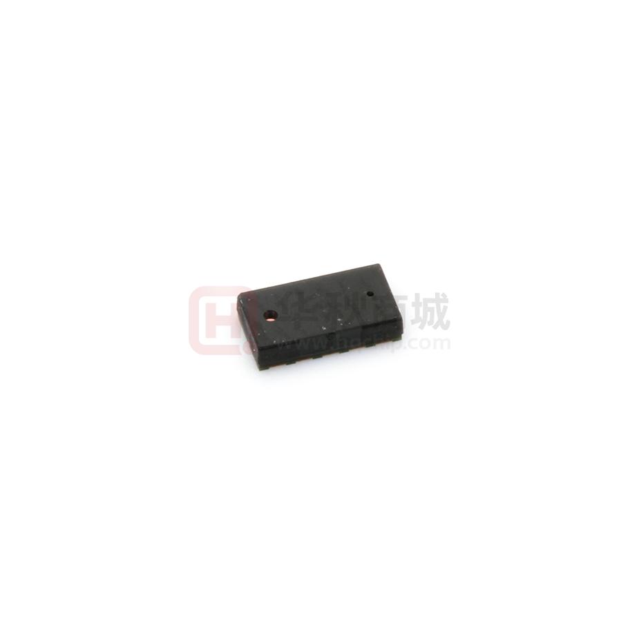
VL53L0X
World’s smallest Time-of-Flight ranging and gesture detection
sensor
Datasheet - production data
Applications
• User detection for personal computers/
laptops/tablets and IoT (energy saving)
• Robotics (obstacle detection)
• White goods (hand detection in automatic
faucets, soap dispensers etc.)
• 1D gesture recognition.
Features
• Fully integrated miniature module
– 940 nm laser VCSEL
– VCSEL driver
– Ranging sensor with advanced embedded
micro controller
– 4.4 x 2.4 x 1.0 mm
• Fast, accurate distance ranging
– Measures absolute range up to 2 m
– Reported range is independent of the
target reflectance
– Advanced embedded optical cross-talk
compensation to simplify cover glass
selection
• Eye safe
– Class 1 laser device compliant with latest
standard IEC 60825-1:2014 - 3rd edition
• Easy integration
– Single reflowable component
– No additional optics
– Single power supply
– I2C interface for device control and data
transfer
– Xshutdown (reset) and interrupt GPIO
– Programmable I2C address
April 2018
This is information on a product in full production.
• Laser assisted autofocus. Enhances and
speeds up camera autofocus system
performance, especially in difficult scenes (low
light levels, low contrast) or fast moving video
mode.
Description
The VL53L0X is a new generation Time-of-Flight
(ToF) laser-ranging module housed in the
smallest package on the market today, providing
accurate distance measurement whatever the
target
reflectances
unlike
conventional
technologies. It can measure absolute distances
up to 2m, setting a new benchmark in ranging
performance levels, opening the door to various
new applications.
The VL53L0X integrates a leading-edge SPAD
array (Single Photon Avalanche Diodes) and
embeds ST’s second generation FlightSenseTM
patented technology.
The VL53L0X’s 940 nm VCSEL emitter (Vertical
Cavity Surface-Emitting Laser), is totally invisible
to the human eye, coupled with internal physical
infrared filters, it enables longer ranging
distances, higher immunity to ambient light, and
better robustness to cover glass optical crosstalk.
DocID029104 Rev 2
1/10
www.st.com
�Contents
VL53L0X
Contents
1
2
Overview . . . . . . . . . . . . . . . . . . . . . . . . . . . . . . . . . . . . . . . . . . . . . . . . . . 6
1.1
Technical specification . . . . . . . . . . . . . . . . . . . . . . . . . . . . . . . . . . . . . . . . 6
1.2
System block diagram . . . . . . . . . . . . . . . . . . . . . . . . . . . . . . . . . . . . . . . . 6
1.3
Device pinout . . . . . . . . . . . . . . . . . . . . . . . . . . . . . . . . . . . . . . . . . . . . . . . 7
1.4
Application schematic . . . . . . . . . . . . . . . . . . . . . . . . . . . . . . . . . . . . . . . . . 8
Functional description . . . . . . . . . . . . . . . . . . . . . . . . . . . . . . . . . . . . . . . 9
2.1
System functional description . . . . . . . . . . . . . . . . . . . . . . . . . . . . . . . . . . . 9
2.2
Firmware state machine description . . . . . . . . . . . . . . . . . . . . . . . . . . . . . 10
2.3
Customer manufacturing calibration flow . . . . . . . . . . . . . . . . . . . . . . . . . .11
2.3.1
SPAD and temperature calibration . . . . . . . . . . . . . . . . . . . . . . . . . . . . 12
2.3.2
Ranging offset calibration . . . . . . . . . . . . . . . . . . . . . . . . . . . . . . . . . . . 12
2.3.3
Cross-talk calibration . . . . . . . . . . . . . . . . . . . . . . . . . . . . . . . . . . . . . . . 13
2.4
Ranging operating modes . . . . . . . . . . . . . . . . . . . . . . . . . . . . . . . . . . . . 13
2.5
Ranging profiles . . . . . . . . . . . . . . . . . . . . . . . . . . . . . . . . . . . . . . . . . . . . 14
2.6
Ranging profile phases . . . . . . . . . . . . . . . . . . . . . . . . . . . . . . . . . . . . . . . 14
2.6.1
Initialization and load calibration data phase . . . . . . . . . . . . . . . . . . . . . 15
2.6.2
Ranging phase . . . . . . . . . . . . . . . . . . . . . . . . . . . . . . . . . . . . . . . . . . . . 15
2.6.3
Digital housekeeping . . . . . . . . . . . . . . . . . . . . . . . . . . . . . . . . . . . . . . . 15
2.7
Getting the data: interrupt or polling . . . . . . . . . . . . . . . . . . . . . . . . . . . . . 16
2.8
Device programming and control . . . . . . . . . . . . . . . . . . . . . . . . . . . . . . . 16
2.9
Power sequence . . . . . . . . . . . . . . . . . . . . . . . . . . . . . . . . . . . . . . . . . . . . 16
2.9.1
2.10
3
4
2/40
Power up and boot sequence . . . . . . . . . . . . . . . . . . . . . . . . . . . . . . . . 16
Ranging sequence . . . . . . . . . . . . . . . . . . . . . . . . . . . . . . . . . . . . . . . . . . 17
Control interface . . . . . . . . . . . . . . . . . . . . . . . . . . . . . . . . . . . . . . . . . . . 18
3.1
I2C interface - timing characteristics . . . . . . . . . . . . . . . . . . . . . . . . . . . . . 20
3.2
I2C interface - reference registers . . . . . . . . . . . . . . . . . . . . . . . . . . . . . . 21
Electrical characteristics . . . . . . . . . . . . . . . . . . . . . . . . . . . . . . . . . . . . 22
4.1
Absolute maximum ratings . . . . . . . . . . . . . . . . . . . . . . . . . . . . . . . . . . . . 22
4.2
Recommended operating conditions . . . . . . . . . . . . . . . . . . . . . . . . . . . . 22
DocID029104 Rev 2
�VL53L0X
5
Contents
4.3
ESD . . . . . . . . . . . . . . . . . . . . . . . . . . . . . . . . . . . . . . . . . . . . . . . . . . . . . 22
4.4
Current consumption . . . . . . . . . . . . . . . . . . . . . . . . . . . . . . . . . . . . . . . . 23
4.5
Electrical characteristics . . . . . . . . . . . . . . . . . . . . . . . . . . . . . . . . . . . . . . 24
Performance . . . . . . . . . . . . . . . . . . . . . . . . . . . . . . . . . . . . . . . . . . . . . . 25
5.1
Measurement conditions . . . . . . . . . . . . . . . . . . . . . . . . . . . . . . . . . . . . . 25
5.2
Max ranging distance . . . . . . . . . . . . . . . . . . . . . . . . . . . . . . . . . . . . . . . . 26
5.3
Ranging accuracy . . . . . . . . . . . . . . . . . . . . . . . . . . . . . . . . . . . . . . . . . . . 27
5.3.1
Standard deviation . . . . . . . . . . . . . . . . . . . . . . . . . . . . . . . . . . . . . . . . . 27
5.3.2
Range profile examples . . . . . . . . . . . . . . . . . . . . . . . . . . . . . . . . . . . . . 28
5.3.3
Ranging offset error . . . . . . . . . . . . . . . . . . . . . . . . . . . . . . . . . . . . . . . . 28
6
Outline drawing . . . . . . . . . . . . . . . . . . . . . . . . . . . . . . . . . . . . . . . . . . . . 29
7
Laser safety considerations . . . . . . . . . . . . . . . . . . . . . . . . . . . . . . . . . . 32
8
Packaging and labeling . . . . . . . . . . . . . . . . . . . . . . . . . . . . . . . . . . . . . 33
8.1
Product marking . . . . . . . . . . . . . . . . . . . . . . . . . . . . . . . . . . . . . . . . . . . . 33
8.2
Inner box labeling . . . . . . . . . . . . . . . . . . . . . . . . . . . . . . . . . . . . . . . . . . . 33
8.3
Packing . . . . . . . . . . . . . . . . . . . . . . . . . . . . . . . . . . . . . . . . . . . . . . . . . . 33
8.3.1
Tape outline drawings . . . . . . . . . . . . . . . . . . . . . . . . . . . . . . . . . . . . . . 34
8.4
Pb-free solder reflow process . . . . . . . . . . . . . . . . . . . . . . . . . . . . . . . . . . 34
8.5
Handling and storage precautions . . . . . . . . . . . . . . . . . . . . . . . . . . . . . . 36
8.6
8.5.1
Shock precaution . . . . . . . . . . . . . . . . . . . . . . . . . . . . . . . . . . . . . . . . . . 36
8.5.2
Part handling . . . . . . . . . . . . . . . . . . . . . . . . . . . . . . . . . . . . . . . . . . . . . 36
8.5.3
Compression force . . . . . . . . . . . . . . . . . . . . . . . . . . . . . . . . . . . . . . . . . 36
8.5.4
Moisture sensitivity level . . . . . . . . . . . . . . . . . . . . . . . . . . . . . . . . . . . . 36
Storage temperature conditions . . . . . . . . . . . . . . . . . . . . . . . . . . . . . . . . 36
9
Ordering information . . . . . . . . . . . . . . . . . . . . . . . . . . . . . . . . . . . . . . . 37
10
Acronyms and abbreviations . . . . . . . . . . . . . . . . . . . . . . . . . . . . . . . . . 37
11
ECOPACK®
12
Revision history . . . . . . . . . . . . . . . . . . . . . . . . . . . . . . . . . . . . . . . . . . . 39
. . . . . . . . . . . . . . . . . . . . . . . . . . . . . . . . . . . . . . . . . . . . . . . . . . . . . . . . . . . . 38
DocID029104 Rev 2
3/40
3
�List of tables
VL53L0X
List of tables
Table 1.
Table 2.
Table 3.
Table 4.
Table 5.
Table 6.
Table 7.
Table 8.
Table 9.
Table 10.
Table 11.
Table 12.
Table 13.
Table 14.
Table 15.
Table 16.
Table 17.
Table 18.
Table 19.
4/40
Technical specification . . . . . . . . . . . . . . . . . . . . . . . . . . . . . . . . . . . . . . . . . . . . . . . . . . . . . 6
VL53L0X pin description . . . . . . . . . . . . . . . . . . . . . . . . . . . . . . . . . . . . . . . . . . . . . . . . . . . . 7
I2C interface - timing characteristics . . . . . . . . . . . . . . . . . . . . . . . . . . . . . . . . . . . . . . . . . 20
Reference registers . . . . . . . . . . . . . . . . . . . . . . . . . . . . . . . . . . . . . . . . . . . . . . . . . . . . . . 21
32-bit register example . . . . . . . . . . . . . . . . . . . . . . . . . . . . . . . . . . . . . . . . . . . . . . . . . . . . 21
Absolute maximum ratings . . . . . . . . . . . . . . . . . . . . . . . . . . . . . . . . . . . . . . . . . . . . . . . . . 22
Recommended operating conditions . . . . . . . . . . . . . . . . . . . . . . . . . . . . . . . . . . . . . . . . . 22
ESD performances . . . . . . . . . . . . . . . . . . . . . . . . . . . . . . . . . . . . . . . . . . . . . . . . . . . . . . . 22
Consumption at ambient temperature . . . . . . . . . . . . . . . . . . . . . . . . . . . . . . . . . . . . . . . . 23
Digital I/O electrical characteristics . . . . . . . . . . . . . . . . . . . . . . . . . . . . . . . . . . . . . . . . . . . 24
Max ranging capabilities with 33ms timing budget . . . . . . . . . . . . . . . . . . . . . . . . . . . . . . . 26
Ranging accuracy . . . . . . . . . . . . . . . . . . . . . . . . . . . . . . . . . . . . . . . . . . . . . . . . . . . . . . . . 27
Range profiles. . . . . . . . . . . . . . . . . . . . . . . . . . . . . . . . . . . . . . . . . . . . . . . . . . . . . . . . . . . 28
Ranging offset. . . . . . . . . . . . . . . . . . . . . . . . . . . . . . . . . . . . . . . . . . . . . . . . . . . . . . . . . . . 28
Recommended solder profile . . . . . . . . . . . . . . . . . . . . . . . . . . . . . . . . . . . . . . . . . . . . . . . 35
Recommended storage conditions . . . . . . . . . . . . . . . . . . . . . . . . . . . . . . . . . . . . . . . . . . . 36
Ordering information . . . . . . . . . . . . . . . . . . . . . . . . . . . . . . . . . . . . . . . . . . . . . . . . . . . . . . 37
Acronyms and abbreviations . . . . . . . . . . . . . . . . . . . . . . . . . . . . . . . . . . . . . . . . . . . . . . . 37
Document revision history . . . . . . . . . . . . . . . . . . . . . . . . . . . . . . . . . . . . . . . . . . . . . . . . . 39
DocID029104 Rev 2
�VL53L0X
List of figures
List of figures
Figure 1.
Figure 2.
Figure 3.
Figure 4.
Figure 5.
Figure 6.
Figure 7.
Figure 8.
Figure 9.
Figure 10.
Figure 11.
Figure 12.
Figure 13.
Figure 14.
Figure 15.
Figure 16.
Figure 17.
Figure 18.
Figure 19.
Figure 20.
Figure 21.
Figure 22.
Figure 23.
Figure 24.
Figure 25.
Figure 26.
Figure 27.
Figure 28.
VL53L0X block diagram . . . . . . . . . . . . . . . . . . . . . . . . . . . . . . . . . . . . . . . . . . . . . . . . . . . . 6
VL53L0X pinout (bottom view) . . . . . . . . . . . . . . . . . . . . . . . . . . . . . . . . . . . . . . . . . . . . . . . 7
VL53L0X schematic . . . . . . . . . . . . . . . . . . . . . . . . . . . . . . . . . . . . . . . . . . . . . . . . . . . . . . . 8
VL53L0X system functional description . . . . . . . . . . . . . . . . . . . . . . . . . . . . . . . . . . . . . . . . 9
Firmware state machine . . . . . . . . . . . . . . . . . . . . . . . . . . . . . . . . . . . . . . . . . . . . . . . . . . . 10
Customer manufacturing calibration flow . . . . . . . . . . . . . . . . . . . . . . . . . . . . . . . . . . . . . . 11
Range offset . . . . . . . . . . . . . . . . . . . . . . . . . . . . . . . . . . . . . . . . . . . . . . . . . . . . . . . . . . . . 12
Cross-talk compensation . . . . . . . . . . . . . . . . . . . . . . . . . . . . . . . . . . . . . . . . . . . . . . . . . . 13
Typical initialization / ranging / housekeeping phases . . . . . . . . . . . . . . . . . . . . . . . . . . . . 14
Power up and boot sequence . . . . . . . . . . . . . . . . . . . . . . . . . . . . . . . . . . . . . . . . . . . . . . . 16
Power up and boot sequence with XSHUT not controlled . . . . . . . . . . . . . . . . . . . . . . . . . 17
Ranging sequence . . . . . . . . . . . . . . . . . . . . . . . . . . . . . . . . . . . . . . . . . . . . . . . . . . . . . . . 17
Data transfer protocol . . . . . . . . . . . . . . . . . . . . . . . . . . . . . . . . . . . . . . . . . . . . . . . . . . . . . 18
VL53L0X I2C device address: 0x52 . . . . . . . . . . . . . . . . . . . . . . . . . . . . . . . . . . . . . . . . . . 18
VL53L0X data format (write) . . . . . . . . . . . . . . . . . . . . . . . . . . . . . . . . . . . . . . . . . . . . . . . . 19
VL53L0X data format (read) . . . . . . . . . . . . . . . . . . . . . . . . . . . . . . . . . . . . . . . . . . . . . . . . 19
VL53L0X data format (sequential write) . . . . . . . . . . . . . . . . . . . . . . . . . . . . . . . . . . . . . . . 19
VL53L0X data format (sequential read) . . . . . . . . . . . . . . . . . . . . . . . . . . . . . . . . . . . . . . . 20
I2C timing characteristics . . . . . . . . . . . . . . . . . . . . . . . . . . . . . . . . . . . . . . . . . . . . . . . . . . 21
Typical ranging (default mode) . . . . . . . . . . . . . . . . . . . . . . . . . . . . . . . . . . . . . . . . . . . . . . 25
Typical ranging - long range mode . . . . . . . . . . . . . . . . . . . . . . . . . . . . . . . . . . . . . . . . . . . 26
Outline drawing (page 1/3) . . . . . . . . . . . . . . . . . . . . . . . . . . . . . . . . . . . . . . . . . . . . . . . . . 29
Outline drawing (page 2/3) . . . . . . . . . . . . . . . . . . . . . . . . . . . . . . . . . . . . . . . . . . . . . . . . . 30
Outline drawing - with liner (page 3/3) . . . . . . . . . . . . . . . . . . . . . . . . . . . . . . . . . . . . . . . . 31
Class 1 laser product label . . . . . . . . . . . . . . . . . . . . . . . . . . . . . . . . . . . . . . . . . . . . . . . . . 32
Example of marking . . . . . . . . . . . . . . . . . . . . . . . . . . . . . . . . . . . . . . . . . . . . . . . . . . . . . . 33
Tape outline drawing . . . . . . . . . . . . . . . . . . . . . . . . . . . . . . . . . . . . . . . . . . . . . . . . . . . . . 34
Solder profile. . . . . . . . . . . . . . . . . . . . . . . . . . . . . . . . . . . . . . . . . . . . . . . . . . . . . . . . . . . . 35
DocID029104 Rev 2
5/40
5
�Overview
VL53L0X
1
Overview
1.1
Technical specification
Table 1. Technical specification
Feature
1.2
Detail
Package
Optical LGA12
Size
4.40 x 2.40 x 1.00 mm
Operating voltage
2.6 to 3.5 V
Operating temperature:
-20 to 70°C
Infrared emitter
940 nm
I2C
Up to 400 kHz (FAST mode) serial bus
Address: 0x52
System block diagram
Figure 1. VL53L0X block diagram
9/��/�;�PRGXOH
9/��/�;�VLOLFRQ
'HWHFWLRQ�DUUD\
*1'
6LQJOH�3KRWRQ
$YDODQFKH�'LRGH��63$'�
6'$
1RQ�9RODWLOH
0HPRU\
520
$9''
;6+87
5$0
6&/
*3,2�
0LFURFRQWUROOHU
$GYDQFHG
5DQJLQJ�&RUH
9&6(/�'ULYHU
$9669&6(/
,5�
,5�
���QP
6/40
DocID029104 Rev 2
$9''9&6(/
�VL53L0X
1.3
Overview
Device pinout
Figure 2 shows the pinout of the VL53L0X (see also Figure 22).
Figure 2. VL53L0X pinout (bottom view)
*1'�
*3,2�
�
'1&
�
�
;6+87
�
�
*1'�
6'$
�
�
*1'
6&/
��
�
$9669&6(/
$9''
��
�
$9''9&6(/
��
*1'�
Table 2. VL53L0X pin description
Pin number
Signal name
Signal type
Signal description
1
AVDDVCSEL
Supply
VCSEL Supply, to be connected to main supply
2
AVSSVCSEL
Ground
VCSEL Ground, to be connected to main ground
3
GND
Ground
To be connected to main ground
4
GND2
Ground
To be connected to main ground
5
XSHUT
Digital input
6
GND3
Ground
7
GPIO1
Digital output
8
DNC
Digital input
Do Not Connect, must be left floating.
9
SDA
Digital
input/output
I2C serial data
10
SCL
Digital input
I2C serial clock input
11
AVDD
Supply
Supply, to be connected to main supply
12
GND4
Ground
To be connected to main ground
Xshutdown pin, Active LOW
To be connected to main ground
Interrupt output. Open drain output.
DocID029104 Rev 2
7/40
37
�Overview
1.4
VL53L0X
Application schematic
Figure 3 shows the application schematic of the VL53L0X.
Figure 3. VL53L0X schematic
,29''
$9''
�
�
+267
�
��
�
;6+87 $9''9&6(/
*3,2�
$9''
6'$
$9669&6(/
6&/
*1'
'1&
*1'�
*1'�
9/��/�;
*1'�
�
��
�
���Q)
���)
�
�
�
��
Note:
Capacitors on external supply AVDD should be placed as close as possible to the
AVDDVCSEL and AVSSVCSEL module pins.
Note:
External pull-up resistors values can be found in I2C-bus specification. Pull-up are typically
fitted only once per bus, near the host.
Recommended values for pull-up resistors for an AVDD of 2.8V and 400KHz I2C clock
would be 1.5k to 2k Ohms.
Note:
XSHUT pin must always be driven to avoid leakage current. Pull-up is needed if the host
state is not known.
XSHUT is needed to use HW standby mode (no I2C comm).
Note:
XSHUT and GPIO1 pull up recommended values are 10k Ohms
Note:
GPIO1 to be left unconnected if not used
8/40
DocID029104 Rev 2
�VL53L0X
Functional description
2
Functional description
2.1
System functional description
Figure 4 shows the system level functional description. The host customer application is
controlling the VL53L0X device using an API (Application Programming Interface).
The API is exposing to the customer application a set of high level functions that allows
control of the VL53L0X Firmware (FW) like initialization/calibration, ranging Start/Stop,
choice of accuracy, choice of ranging mode.
The API is a turnkey solution, it consists of a set of C functions which enables fast
development of end user applications, without the complication of direct multiple register
access. The API is structured in a way that it can be compiled on any kind of platform
through a well isolated platform layer.
The API package allows the user to take full benefit of VL53L0X capabilities.
A detailed description of the API is available in the VL53L0X API User Manual (separate
document, DocID029105).
VL53L0X FW fully manages the hardware (HW) register accesses.
Section 2.2: Firmware state machine description details the Firmware state machine.
Figure 4. VL53L0X system functional description
+267
&XVWRPHU
$SSOLFDWLRQ
9/��/�;
9/��/�;
$3,
)LUPZDUH
+DUGZDUH
,�&
DocID029104 Rev 2
9/40
37
�Functional description
2.2
VL53L0X
Firmware state machine description
Figure 5 shows the Firmware state machine.
Figure 5. Firmware state machine
3RZHU�2II
+RVW�DSSOLHV�$9''
+RVW�UHPRYHV�$9''
+Z�6WDQGE\
+RVW�ORZHUV�;6+87
+RVW�UDLVHV�;6+87
)Z�,QLWLDO�%RRW
+RVW�LQLWLDWHV�6723
$XWRPDWLF�PRYH�WR�6:�VWDQGE\
6Z�6WDQGE\
+RVW�LQLWLDWHV�67$57
5DQJH�0RGH
&RQWLQXRXV�7LPHG
&RQWLQXRXV
6LQJOH
5DQJH�0HDV
5DQJH�0HDV
5DQJH�0HDV
1H[W�VWDUW�VWDUWV�
DXWRPDWLFDOO\�DIWHU�
WKH�ODVW�KDV�ILQLVKHG
,QWHU�0HDV
6WDQGE\
,QWHU�PHDVXUHPHQW�
SHULRG�QRW�FRPSOHWHG
10/40
DocID029104 Rev 2
�VL53L0X
2.3
Functional description
Customer manufacturing calibration flow
Figure 6 shows the recommended calibration flow that should be applied at customer level,
at factory, once only. This flow takes into account all parameters (cover glass, temperature &
voltage) from the application.
Figure 6. Customer manufacturing calibration flow
DĂŶƵĨĂĐƚƵƌŝŶŐ
ĐĂůŝďƌĂƚŝŽŶ�ĨůŽǁ
�ĞǀŝĐĞ�ŝŶŝƚŝĂůŝnjĂƚŝŽŶ�ĂŶĚ�ƐĞƚƚŝŶŐƐ�
;ΕϰϬŵƐΎͿ
^W��Ɛ�ĐĂůŝďƌĂƚŝŽŶ�;ΕϭϬŵƐΎͿ
dĞŵƉĞƌĂƚƵƌĞ�ĐĂůŝďƌĂƚŝŽŶ�;ΕϰϬŵƐΎͿ
KĨĨƐĞƚ�ĐĂůŝďƌĂƚŝŽŶ�;ΕϯϬϬŵƐΎͿ
�ƌŽƐƐdĂůŬ�ĐĂůŝďƌĂƚŝŽŶ�;ΕϭƐĞĐΎͿ
Ύ�͗�dŝŵŝŶŐƐ�ĂƌĞ�ŐŝǀĞŶ�ĨŽƌ�ŝŶĨŽƌŵĂƚŝŽŶ�ŽŶůLJ͕�ƚŚĞLJ�
ĐĂŶ�ǀĂƌLJ�ĚĞƉĞŶĚŝŶŐ�ŽŶ�ƚŚĞ�,ŽƐƚ�ĐĂƉĂďŝůŝƚŝĞƐ
/ŶŝƚŝĂůŝƐĂƚŝŽŶ�Ͳ
�ƚŽ�ďĞ�ĐĂůůĞĚ�ŽŶĐĞ�ĂĨƚĞƌ�ĚĞǀŝĐĞ�ƌĞƐĞƚ
/ŶŝƚŝĂů�ĐĂůŝďƌĂƚŝŽŶ�Ͳ�ƌĞƋƵŝƌĞĚ�ŽŶůLJ�ŽŶĐĞ͕�
ŚŽƐƚ�ƚŽ�ƐƚŽƌĞ�ǀĂůƵĞƐ͘��
�ĂůŝďƌĂƚŝŽŶ�ƐƚĞƉ�ƚŽ�ďĞ�ƌĞƉĞĂƚĞĚ�ǁŝƚŚ�
х�ϴ�ĚĞŐƌĞĞ��ƚĞŵƉĞƌĂƚƵƌĞ�ĐŚĂŶŐĞ͘
DocID029104 Rev 2
11/40
37
�Functional description
2.3.1
VL53L0X
SPAD and temperature calibration
In order to optimize the dynamic of the system, the reference SPADs have to be calibrated.
Reference SPAD calibration needs to be done only once during the initial manufacturing
calibration, the calibration data should then be stored on the Host.
Temperature calibration is the calibration of two parameters (VHV and phase cal) which are
temperature dependent. These two parameters are used to set the device sensitivity.
Calibration should be performed during initial manufacturing calibration, it must be
performed again when temperature varies more than 8degC compared to the initial
calibration temperature.
For more details on SPAD and temperature calibration please refer to the VL53L0X API
User Manual.
2.3.2
Ranging offset calibration
Ranging offset can be characterized by the mean offset, which is the centering of the
measurement versus the real distance.
Offset calibration should be performed at factory for optimal performances (recommended
at 10cm). The offset calibration should take into account:
•
Supply voltage and temperature
•
Protective cover glass above VL53L0X module
Measured range
Figure 7. Range offset
p2p_offset
calibration
Actual Range
12/40
DocID029104 Rev 2
�VL53L0X
2.3.3
Functional description
Cross-talk calibration
Cross-talk is defined as the signal return from the cover glass. The magnitude of the crosstalk depends on the type of glass and air gap. Cross-talk results in a range error which is
proportional to the ratio of the cross-talk to the signal return from the target.
Measured range
Figure 8. Cross-talk compensation
cross-talk
compensation
Actual Range
Full offset and cross-talk calibration procedure is described in the VL53L0X API User
Manual.
2.4
Ranging operating modes
There are 3 ranging modes available in the API:
1.
Single ranging
Ranging is performed only once after the API function is called.
System returns to SW standby automatically.
2.
Continuous ranging
Ranging is performed in a continuous way after the API function is called. As soon as
the measurement is finished, another one is started without delay.
User has to stop the ranging to return to SW standby. The last measurement is
completed before stopping.
3.
Timed ranging
Ranging is performed in a continuous way after the API function is called. When a
measurement is finished, another one is started after a user defined delay.
This delay (inter-measurement period) can be defined through the API.
User has to stop the ranging to return to SW standby.
If the stop request comes during a range measurement, the measurement is completed
before stopping. If it happens during an inter-measurement period, the range measurement
stops immediately.
DocID029104 Rev 2
13/40
37
�Functional description
2.5
VL53L0X
Ranging profiles
There are 4 different ranging profiles available via API example code. Customers can create
their own ranging profile dependent on their use case performance requirements.
For more details please refer to the VL53L0X API User Manual.
2.6
1.
Default mode
2.
High speed
3.
High accuracy
4.
Long range
Ranging profile phases
Each range profile consists of 3 consecutive phases:
•
Initialization and load calibration data
•
Ranging
•
Digital housekeeping
Figure 9. Typical initialization / ranging / housekeeping phases
/ŶŝƚŝĂůŝnjĂƚŝŽŶ�ĂŶĚ��ĂůŝďƌĂƚŝŽŶ�
;ƚŽ�ďĞ�ĐĂůůĞĚ�ĂĨƚĞƌ�ĚĞǀŝĐĞ�
ƌĞƐĞƚͿ
�ĞǀŝĐĞ�ŝŶŝƚŝĂůŝnjĂƚŝŽŶ�ĂŶĚ�ƐĞƚƚŝŶŐƐ�
;ΕϰϬŵƐΎͿ
>ŽĂĚ�ĐĂůŝďƌĂƚŝŽŶ��ĚĂƚĂ�;ΕϭŵƐΎͿ�
/ŶĐůƵĚĞƐ�;^Ğƚ^W���ĂůŝďƌĂƚŝŽŶ͕�
^ĞƚdĞŵƉ�ĂůŝďƌĂƚŝŽŶ͕�
^ĞƚKĨĨƐĞƚ�ĂůŝďƌĂƚŝŽŶ�Θ
^Ğƚ�ƌŽƐƐͲƚĂůŬsĂůƵĞͿ
ZĂŶŐĞ�ƐĞƚ�ƵƉ�;ΕϴŵƐΎͿ
ZĂŶŐŝŶŐ
ZĂŶŐĞ�ŵĞĂƐƵƌĞŵĞŶƚ��;ΕϮϯŵƐΎͿ
�ŝŐŝƚĂů
ŚŽƵƐĞŬĞĞƉŝŶŐ
�ŝŐŝƚĂů�ƉƌŽĐĞƐƐŝŶŐ�;ΕϬ͘ϴŵƐΎͿ
Ύ�͗�dŝŵŝŶŐƐ�ĂƌĞ�ŐŝǀĞŶ�ĨŽƌ�ŝŶĨŽƌŵĂƚŝŽŶ�ŽŶůLJ͕�ƚŚĞLJ�
ĐĂŶ�ǀĂƌLJ�ĚĞƉĞŶĚŝŶŐ�ŽŶ�ƚŚĞ�,ŽƐƚ�ĐĂƉĂďŝůŝƚŝĞƐ
14/40
DocID029104 Rev 2
�VL53L0X
2.6.1
Functional description
Initialization and load calibration data phase
Initialization and calibration phase is performed before the first ranging or after a device
reset, see Figure 9.
The user may then have to repeat the temperature calibration phase in a periodic way,
depending on the use case.
For more details on the calibration functions please refer to the VL53L0X API User Manual.
2.6.2
Ranging phase
The ranging phase consists of a range setup then range measurement.
During the ranging operation, several VCSEL infrared pulses are emitted, then reflected
back by the target object, and detected by the receiving array. The photo detector used
inside VL53L0X is using advanced ultra-fast SPAD technology (Single Photon Avalanche
Diodes), protected by several patents.
The typical timing budget for a range is 33ms (init/ranging/housekeeping), see Figure 12,
with the actual range measurement taking 23ms, see Figure 9. The minimum range
measurement period is 8ms.
2.6.3
Digital housekeeping
Digital processing (housekeeping) is the last operation inside the ranging sequence that
computes, validates or rejects a ranging measurement. Part of this processing is performed
internally while the other part is executed on the Host by the API.
At the end of the digital processing, the ranging distance is computed by VL53L0X itself. If
the distance could not be measured (weak signal, no target…), a corresponding error code
is provided.
The following functions are performed on the device itself:
• Signal value check (weak signal)
• Offset correction
• Cross-talk correction (in case of cover glass)
• Final ranging value computation
While the API performs the following:
• Return Ignore Threshold RIT check (Signal check versus cross talk)
• Sigma check (accuracy condition)
• Final ranging state computation
If the user wants to enhance the ranging accuracy, some extra processing (not part of the
API) can be carried out by the host, for example, rolling average, hysteresis or any kind of
filtering.
DocID029104 Rev 2
15/40
37
�Functional description
2.7
VL53L0X
Getting the data: interrupt or polling
User can get the final data using a polling or an interrupt mechanism.
Polling mode: user has to check the status of the ongoing measurement by polling an API
function.
Interrupt mode: An interrupt pin (GPIO1) sends an interrupt to the host when a new
measurement is available.
The description of these 2 modes is available in the VL53L0X API User Manual.
2.8
Device programming and control
Device physical control interface is I2C, described in Section 3: Control interface.
A software layer (API) is provided to control the device. The API is described in the
VL53L0X API User Manual.
2.9
Power sequence
2.9.1
Power up and boot sequence
There are two options available for device power up/boot.
Option 1: XSHUT pin connected and controlled from host.
This option helps to optimize power consumption as the VL53L0X can be completely
powered off when not used, and then woken up through host GPIO (using XSHUT pin).
HW Standby mode is defined as the period when AVDD is present and XSHUT is low.
Figure 10. Power up and boot sequence
tBOOT is 1.2ms max.
Option 2: XSHUT pin not controlled by host, and tied to AVDD through pull-up resistor.
In case XSHUT pin is not controlled, the power up sequence is presented in Figure 11. In
this case, the device is going automatically in SW STANDBY after FW BOOT, without
entering HW STANDBY.
16/40
DocID029104 Rev 2
�VL53L0X
Functional description
Figure 11. Power up and boot sequence with XSHUT not controlled
tBOOT is 1.2ms max.
2.10
Ranging sequence
Figure 12. Ranging sequence
ttiming_budget is a parameter set by the user, using a dedicated API function.
Default value is 33ms.
DocID029104 Rev 2
17/40
37
�Control interface
3
VL53L0X
Control interface
This section specifies the control interface. The I2C interface uses two signals: serial data
line (SDA) and serial clock line (SCL). Each device connected to the bus is using a unique
address and a simple master / slave relationships exists.
Both SDA and SCL lines are connected to a positive supply voltage using pull-up resistors
located on the host. Lines are only actively driven low. A high condition occurs when lines
are floating and the pull-up resistors pull lines up. When no data is transmitted both lines are
high.
Clock signal (SCL) generation is performed by the master device. The master device
initiates data transfer. The I2C bus on the VL53L0X has a maximum speed of 400 kbits/s
and uses a device address of 0x52.
Figure 13. Data transfer protocol
Acknowledge
Start condition
SDA
MSB
SCL
S
1
LSB
2
3
4
5
8
7
6
Address or data byte
Ac/Am
P
Stop condition
Information is packed in 8-bit packets (bytes) always followed by an acknowledge bit, Ac for
VL53L0X acknowledge and Am for master acknowledge (host bus master). The internal
data is produced by sampling SDA at a rising edge of SCL. The external data must be stable
during the high period of SCL. The exceptions to this are start (S) or stop (P) conditions
when SDA falls or rises respectively, while SCL is high.
A message contains a series of bytes preceded by a start condition and followed by either a
stop or repeated start (another start condition but without a preceding stop condition)
followed by another message. The first byte contains the device address (0x52) and also
specifies the data direction. If the least significant bit is low (that is, 0x52) the message is a
master write to the slave. If the lsb is set (that is, 0x53) then the message is a master read
from the slave.
Figure 14. VL53L0X I2C device address: 0x52
LSBit
MSBit
0
1
0
1
0
0
1
R/W
All serial interface communications with the camera module must begin with a start
condition. The VL53L0X module acknowledges the receipt of a valid address by driving the
SDA wire low. The state of the read/write bit (lsb of the address byte) is stored and the next
byte of data, sampled from SDA, can be interpreted. During a write sequence the second
byte received provide a 8-bit index which points to one of the internal 8-bit registers.
18/40
DocID029104 Rev 2
�VL53L0X
Control interface
Figure 15. VL53L0X data format (write)
VL53L0X acknowledges
Start
S
valid address
ADDRESS[7:0]
Ac
INDEX[7:0]
Acknowledge from VL53L0X
Ac
DATA[7:0]
0x52 (write)
Ac P
Stop
As data is received by the slave it is written bit by bit to a serial/parallel register. After each
data byte has been received by the slave, an acknowledge is generated, the data is then
stored in the internal register addressed by the current index.
During a read message, the contents of the register addressed by the current index is read
out in the byte following the device address byte. The contents of this register are parallel
loaded into the serial/parallel register and clocked out of the device by the falling edge of
SCL.
Figure 16. VL53L0X data format (read)
0x52 (write)
S
ADDRESS[7:0]
Ac
INDEX[7:0]
Ac P
0x53 (read)
S
ADDRESS[7:0]
Ac
DATA[7:0]
Am P
At the end of each byte, in both read and write message sequences, an acknowledge is
issued by the receiving device (that is, the VL53L0X for a write and the host for a read).
A message can only be terminated by the bus master, either by issuing a stop condition or
by a negative acknowledge (that is, not pulling the SDA line low) after reading a complete
byte during a read operation.
The interface also supports auto-increment indexing. After the first data byte has been
transferred, the index is automatically incremented by 1. The master can therefore send
data bytes continuously to the slave until the slave fails to provide an acknowledge or the
master terminates the write communication with a stop condition. If the auto-increment
feature is used the master does not have to send address indexes to accompany the data
bytes.
Figure 17. VL53L0X data format (sequential write)
0x52 (write)
S
ADDRESS[7:0]
Ac
INDEX[7:0]
DATA[7:0]
Ac
DATA[7:0]
Ac
DocID029104 Rev 2
Ac
DATA[7:0]
Ac P
19/40
37
�Control interface
VL53L0X
Figure 18. VL53L0X data format (sequential read)
0x52 (write)
ADDRESS[7:0]
S
INDEX[7:0]
Ac
Ac P
0x53 (read)
S
ADDRESS[7:0]
DATA[7:0]
3.1
DATA[7:0]
Ac
Am
DATA[7:0]
Am
DATA[7:0]
Am
DATA[7:0]
Am
Am P
I2C interface - timing characteristics
Timing characteristics are shown in Table 3. Please refer to Figure 19 for an explanation of
the parameters used.
Timings are given for all PVT conditions.
Table 3. I2C interface - timing characteristics
Symbol
Parameter
Minimum
Typical
Maximum
Unit
0
-
400(1)
kHz
FI2C
Operating frequency (Standard and
Fast mode)
tLOW
Clock pulse width low
1.3
-
-
μs
tHIGH
Clock pulse width high
0.6
-
-
μs
tSP
Pulse width of spikes which are
suppressed by the input filter
-
-
50
ns
tBUF
Bus free time between transmissions
1.3
-
-
ms
tHD.STA
Start hold time
0.26
-
-
μs
tSU.STA
Start set-up time
0.26
-
-
μs
tHD.DAT
Data in hold time
0
-
0.9
μs
tSU.DAT
Data in set-up time
50
-
-
ns
tR
SCL/SDA rise time
-
-
120
ns
tF
SCL/SDA fall time
-
-
120
ns
tSU.STO
Stop set-up time
0.6
-
-
μs
Ci/o
Input/output capacitance (SDA)
-
-
10
pF
Cin
Input capacitance (SCL)
-
-
4
pF
CL
Load capacitance
-
125
400
pF
1. The maximum bus speed is also limited by the combination of 400pF load capacitance and pull-up resistor.
Please refer to the I2C specification for further information.
20/40
DocID029104 Rev 2
�VL53L0X
Control interface
Figure 19. I2C timing characteristics
stop
start
start
...
SDA
tBUF
SCL
tLOW
tR
VIH
VIL
tHD.STA
tF
VIH
stop
...
VIL
tHD.STA
tHD.DAT
tHIGH
tSU.DAT
tSU.STA
tSU.STO
All timings are measured from either VIL or VIH.
3.2
I2C interface - reference registers
The registers shown in the table below can be used to validate the user I2C interface.
Table 4. Reference registers
Note:
Address
(After fresh reset, without API loaded)
0xC0
0xEE
0xC1
0xAA
0xC2
0x10
0x51
0x0099
0x61
0x0000
I2C read/writes can be 8,16 or 32-bit. Multi-byte reads/writes are always addressed in
ascending order with MSB first as shown in Table 5.
Table 5. 32-bit register example
Register address
Byte
Address
MSB
Address + 1
..
Address + 2
..
Address + 3
LSB
DocID029104 Rev 2
21/40
37
�Electrical characteristics
VL53L0X
4
Electrical characteristics
4.1
Absolute maximum ratings
Table 6. Absolute maximum ratings
Parameter
Min.
Typ.
Max.
Unit
AVDD
-0.5
-
3.6
V
SCL, SDA, XSHUT and GPIO1
-0.5
-
3.6
V
Note:
Stresses above those listed in Table 6. may cause permanent damage to the device. This is
a stress rating only and functional operation of the device at these or any other conditions
above those indicated in the operational sections of the specification is not implied.
Exposure to absolute maximum rating conditions for extended periods may affect device
reliability.
4.2
Recommended operating conditions
Table 7. Recommended operating conditions(1)
Parameter
Min.
Typ.
Max.
Unit
2.6
2.8
3.5
V
Standard mode
1.6
1.8
1.9
V
mode(3)(4)
2.6
2.8
3.5
V
+70
°C
Voltage (AVDD)
IO (IOVDD)(2)
2V8
Temperature (normal operating)
-20
1. There are no power supply sequencing requirements. The I/Os may be high, low or floating when AVDD is
applied. The I/Os are internally failsafe with no diode connecting them to AVDD
2. XSHUT should be high level only when AVDD is on.
3. SDA, SCL, XSHUT and GPIO1 high levels have to be equal to AVDD in 2V8 mode.
4. The default API mode is 1V8.
2V8 mode is programmable using device settings loaded by the API. For more details please refer to the
VL53L0X API User Manual.
4.3
ESD
VL53L0X is compliant with ESD values presented inTable 8
Table 8. ESD performances
22/40
Parameter
Specification
Conditions
Human Body Model
JS-001-2012
+/- 2kV, 1500 Ohms, 100pF
Charged Device Model
JZSD22-C101
+/- 500V
DocID029104 Rev 2
�VL53L0X
4.4
Electrical characteristics
Current consumption
Table 9. Consumption at ambient temperature(1)
Parameter
Min.
Typ.
Max.
Unit
HW STANDBY
3
5
7
uA
SW STANDBY (2V8 mode)(2)
4
6
9
uA
Timed ranging Inter measurement
16
uA
Active Ranging average consumption
(including VCSEL) (3)(4)
19
mA
Average power consumption at 10Hz
with 33ms ranging sequence
20
mW
1. All current consumption values include silicon process variations. Temperature and Voltage are at nominal
conditions (23degC and 2.8V).
All values include AVDD and AVDDVCSEL.
2. In standard mode (1V8), pull-ups have to be modified, then SW STANDBY consumption is increased by
+0.6uA.
3. Active ranging is an average value, measured using default API settings (33ms timing budget).
4. Peak current (including VCSEL) can reach 40mA.
DocID029104 Rev 2
23/40
37
�Electrical characteristics
4.5
VL53L0X
Electrical characteristics
Table 10. Digital I/O electrical characteristics
Symbol
Parameter
Minimum
Typical
Maximum
Unit
Interrupt pin (GPIO1)
VIL
Low level input voltage
-
-
0.3 IOVDD
V
VIH
High level input voltage
0.7 IOVDD
-
-
V
VOL
Low level output voltage
(IOUT = 4 mA)
-
-
0.4
V
VOH
High level output voltage at
(IOUT = 4 mA)
IOVDD0.4
-
-
V
FGPIO
Operating frequency
(CLOAD = 20 pF)
0
-
108
MHz
I2C interface (SDA/SCL)
VIL
Low level input voltage
-0.5
-
0.6
V
VIH
High level input voltage
1.12
-
IOVDD+0.5
V
VOL
Low level output voltage (IOUT = 4 mA
in Standard and Fast modes)
-
-
0.4
V
Leakage current(1)
-
-
10
µA
Leakage current(2)
-
-
0.15
µA
IIL/IH
1. AVDD = 0 V
2. AVDD = 2.85 V; I/O voltage = 1.8 V
24/40
DocID029104 Rev 2
�VL53L0X
Performance
5
Performance
5.1
Measurement conditions
In all measurement tables in the document, it is considered that the full Field Of View (FOV)
is covered.
VL53L0X system FOV is 25degrees.
Reflectance targets are standard ones (Grey 17% N4.74 and White 88% N9.5 Munsell
charts).
Unless mentioned, device is controlled through the API using the default settings (refer to
VL53L0X API User Manual for API settings description).
Figure 20. Typical ranging (default mode)
API_RangeValue (mm) vs. Actual Target Distance (mm)
Reflectance
1200
grey17
white88
1100
1000
900
800
700
600
500
400
300
200
100
0
0
100
200
300
400
500
600
700
800
Actual Target Distance (mm)
DocID029104 Rev 2
900
1000
1100
1200
25/40
37
�Performance
VL53L0X
Figure 21. Typical ranging - long range mode
API_RangeValue (mm) vs. Actual Target Distance (mm)
Reflectance
grey17
white88
2200
2000
1800
1600
1400
1200
1000
800
600
400
200
0
5.2
0
200
400
600
800
1000
1200
1400
Actual Target Distance (mm)
1600
1800
2000
2200
2400
Max ranging distance
Table 11 presents the ranging specification for VL53L0X bare module, without cover glass,
at room temperature (23degreesC) and with nominal voltage (2.8Volts).
Table 11. Max ranging capabilities with 33ms timing budget
Target reflectance level
(full FOV)
White target (88%)
Grey target (17%)
Conditions
Indoor
(2)
Outdoor overcast
(2)
Typical
200cm+ (1)
80cm
Minimum
120cm
60cm
Typical
80cm
50cm
Minimum
70cm
40cm
Note (1): using long range API profile
26/40
DocID029104 Rev 2
�VL53L0X
Performance
Note (2):
–
Indoor: no infrared
–
Outdoor overcast corresponds to a parasitic noise of 10kcps/SPAD for VL53L0X
module. For reference, this corresponds to a 1.2W/m² at 940nm, and is equivalent
to 5kLux daylight, while ranging on a grey 17% chart at 40cm
Measurement conditions:
–
Targets reflectance used : Grey (17%), White (88%)
–
Nominal Voltage (2.8V) and Temperature (23degreesC)
–
All distances are for a complete Field of View covered (FOV = 25degrees)
–
33ms timing budget
All distances mentioned in this table are guaranteed for a minimum detection rate of 94%
(up to 100%). Detection rate is the worst case percentage of measurements that will return a
valid measurement when target is detected.
5.3
Ranging accuracy
5.3.1
Standard deviation
Ranging accuracy can be characterized by standard deviation. It includes Measure-toMeasure and Part-to-Part (silicon) dispersion.
Table 12. Ranging accuracy
Indoor (no infrared)
Outdoor
Target reflectance
level (full FOV)
Distance
33 ms
66 ms
Distance
33 ms
66 ms
White Target (88%)
At 120 cm
4%
3%
At 60 cm
7%
6%
Grey Target (17%)
At 70 cm
7%
6%
at 40 cm
12 %
9%
Measurement conditions:
–
Targets reflectance used: Grey (17 %), White (88 %)
–
Offset correction done at 10 cm from sensor
–
Indoor: no infrared / Outdoor: eq. 5 kLux equivalent sunlight (10 kcps/SPAD)
–
Nominal voltage (2v8) and Temperature (23 degreesC)
–
All distances are for a complete FOV covered (FOV = 25 degrees)
–
Detection rate is considered at 94 % minimum
DocID029104 Rev 2
27/40
37
�Performance
5.3.2
VL53L0X
Range profile examples
Table 13 details typical performance for the four example ranging profiles, as per
measurement conditions in Section 5.3: Ranging accuracy.
Table 13. Range profiles
5.3.3
Range profile
Range timing budget
Typical performance
Typical application
Default mode
30 ms
1.2 m, accuracy as per
Table 12
Standard
High accuracy
200 ms
1.2 m, accuracy < +/- 3 %
Precise measurement
Long range
33 ms
2 m, accuracy as per
Table 12
Long ranging, only for
dark conditions (no IR)
High speed
20 ms
1.2 m, accuracy +/- 5 %
High speed where
accuracy is not priority
Ranging offset error
The table below shows how range offset may drift over distance, voltage and temperature.
Assumes offset calibrated at 10cm. See VL53L0X API User Manual for details on offset
calibration.
Table 14. Ranging offset
28/40
Nominal
conditions
Measure point
Ranging
distance
Offset calibration
at 10 cm (“zero”)
White 120 cm (indoor)
Grey 70 cm (indoor)
White 60 cm (outdoor)
Grey 40 cm (outdoor)
Voltage drift
2.8 V
2.6 V to 3.5 V
+/- 10 mm
+/- 15 mm
Temperature
drift
23 °C
-20°C to +70°C
+/- 10 mm
+/- 30 mm
DocID029104 Rev 2
Typical offset
from nominal
Maximum offset
from nominal