VN02NSP VN02NPT
HIGH SIDE SMART POWER SOLID STATE RELAY
PRELIMINARY DATA TYPE VN02NSP VN02NPT
s
V DSS 60 V 60 V
R DS(on ) 0.4 Ω 0.4 Ω
I OUT 6A 6A
V CC 26 V 26 V
s s s s s
OUTPUT CURRENT (CONTINUOUS): 6A @ Tc=25oC 5V LOGIC LEVEL COMPATIBLE INPUT THERMAL SHUT-DOWN UNDER VOLTAGE SHUT-DOWN OPEN DRAIN DIAGNOSTIC OUTPUT VERY LOW STAND-BY POWER DISSIPATION
10
1
DESCRIPTION The VN02NSP/VN02NPT are monolithic devices made using SGS-THOMSON Vertical Intelligent Power Technology, intended for driving resistive or inductive loads with one side grounded. Built-in thermal shut-down protects the chip from over temperature and short circuit. The input control is 5V logic level compatible. BLOCK DIAGRAM
PowerSO-10TM
PPAK
The open drain diagnostic output indicates open circuit (no load) and over temperature status.
September 1997
1/10
�VN02NSP/VN02NPT
ABSOLUTE MAXIMUM RATING
Symbol Parameter Value PowerSO-10 V (BR)DSS I OUT IR I IN -V CC I STAT V ESD P tot Tj T stg Drain-Source Breakdown Voltage Output Current (cont.) Reverse Output Current Input Current Reverse Supply Voltage Status Current Electrostatic Discharge (1.5 k Ω , 100 pF) Power Dissipation at T c ≤ 2 5 C
o
Unit PPAK
60 6 -6 ± 10 -4 ± 10 2000 58 -40 to 150 -55 to 150 46
V A A mA V mA V W
o o
Junction Operating Temperature Storage Temperature
C C
CONNECTION DIAGRAMS
CURRENT AND VOLTAGE CONVENTIONS
2/10
�VN02NSP/VN02NPT
THERMAL DATA
PowerSO-10 R thj-case R thj-amb Thermal Resistance Junction-case Thermal Resistance Junction-ambient ($) Max Max 2.14 62.5 PPAK 3.33 100
o o
C/W C/W
($) When mounted using minimum recommended pad size on FR-4 board
ELECTRICAL CHARACTERISTICS (VCC = 13 V; -40 ≤ Tj ≤ 125 oC unless otherwise specified) POWER
Symbol VCC R on IS Parameter Supply Voltage On State Resistance Supply Current I OUT = 3 A I OUT = 3 A Off State On State T j = 25 oC T j ≥ 25 oC Test Conditions Min. 7 Typ. Max. 26 0.8 0.4 50 15 Unit V Ω Ω µA mA
SWITCHING
Symbol t d(on) tr t d(off) tf (di/dt) on (di/dt) off Parameter Turn-on Delay Time Of Output Current Rise Time Of Output Current Turn-off Delay Time Of Output Current Fall Time Of Output Current Turn-on Current Slope Turn-off Current Slope Test Conditions I OUT = 3 A R esistive Load o Input Rise Time < 0.1 µ s T j = 2 5 C I OUT = 3 A R esistive Load o Input Rise Time < 0.1 µ s T j = 2 5 C I OUT = 3 A R esistive Load o Input Rise Time < 0.1 µ s T j = 2 5 C I OUT = 3 A R esistive Load o Input Rise Time < 0.1 µ s T j = 2 5 C I OUT = 3 A I OUT = IOV I OUT = 3 A I OUT = IOV Min. Typ. 10 15 15 6 0 .5 2 2 4 Max. Unit µs µs µs µs A/ µ s A/ µ s A/ µ s A/ µ s
LOGIC INPUT
Symbol V IL VIH V I(hyst.) I IN V ICL Parameter Input Low Level Voltage Input High Level Voltage Input Hysteresis Voltage Input Current Input Clamp Voltage V IN = 5 V I IN = 1 0 mA I IN = - 10 mA 2 0.5 250 6 -0.7 500 Test Conditions Min. Typ. Max. 0.8 (*) Unit V V V µA V V
3/10
�VN02NSP/VN02NPT
ELECTRICAL CHARACTERISTICS (continued) PROTECTION AND DIAGNOSTICS
Symbol V STAT (• ) V USD V SCL ( ) t SC Parameter Status Voltage Output Low Under Voltage Shut Down Status Clamp Voltage Switch-off Time in Short Circuit Condition at Start-Up Over Current Average Current in Short Circuit Open Load Current Level Thermal Shut-down Temperature Reset Temperature I STAT = 1 0 mA I STAT = -10 mA R LOAD < 1 0 m Ω T c = 2 5 o C Test Conditions I STAT = 1.6 mA 6.5 6 -0.7 1.5 5 Min. Typ. Max. 0.4 Unit V V V V ms
I OV I AV I OL T TSD TR
R LOAD < 1 0 m Ω - 40 T c 1 25 o C R LOAD < 1 0 m Ω T c = 8 5 C
o
28 0.9 5 140 125 70
A A mA
o
C C
o
(*) The VIH is internally clamped at 6V about. It is possible to connect this pin to an higher voltage via an external resistor calculated to not exceed 10 mA at the input pin. @NOTE = () Status determination > 100 µs after the switching edge.
FUNCTIONAL DESCRIPTION The device has a diagnostic output which indicates open circuit (no load) and over temperature conditions. The output signals are processed by internal logic. To protect the device against short circuit and over-current condition, the thermal protection turns the integrated Power MOS off at a minimum junction temperature of 140 oC. When the temperature returns to about 125 oC the switch is automatically turned on again. In short circuit conditions the protection reacts with virtually no delay, the sensor being located in the region of the die where the heat is generated. PROTECTING THE DEVICE AGAINST REVERSE BATTERY The simplest way to protect the device against a continuous reverse battery voltage (-26V) is to insert a Schottky diode between pin 1 (GND) and ground, as shown in the typical application circuit (fig. 3).
The consequences of the voltage drop across this diode are as follows:
- If the input is pulled to power GND, a negative
voltage of -VF is seen by the device. (VIL, VIH thresholds and VSTAT are increased by VF with respect to power GND). The undervoltage shutdown level is increased by VF. If there is no need for the control unit to handle external analog signals referred to the power GND, the best approach is to connect the reference potential of the control unit to node [1] (see application circuit infig. 4), which becomes the common signal GND for the whole control board. In this way no shift of VIH, VIL and VSTAT takes place and no negative voltage appears on the INPUT pin; this solution allows the use of a standard diode, with a breakdown voltage able to handle any ISO normalized negative pulses that occours in the automotive environment.
4/10
�VN02NSP/VN02NPT
TRUTH TABLE
INPUT Normal Operation Open Circuit (No Load) Over-temperature Under-voltage L H H H X OUTPUT L H H L L DIAGNOSTIC H H L L H
Figure 1: Waveforms
Figure 2: Over Current Test Circuit
5/10
�VN02NSP/VN02NPT
Figure 3: Typical Application Circuit With A Schottky Diode For Reverse Supply Protection
Figure 4: Typical Application Circuit With Separate Signal Ground
6/10
�VN02NSP/VN02NPT
RDS(on) vs Junction Temperature RDS(on) Vs Supply Voltage
RDS(on) Vs Output Current
Input Voltage vs Junction Temperature
Output Current Derating
Open Load vs Junction Temperature
7/10
�VN02NSP/VN02NPT
PowerSO-10 MECHANICAL DATA
DIM. MIN. A A1 B c D D1 E E1 E2 E3 E4 e F H h L q α 0o 1.20 1.70 8o 1.25 13.80 0.50 1.80 0.047 0.067 3.35 0.00 0.40 0.35 9.40 7.40 9.30 7.20 7.20 6.10 5.90 1.27 1.35 14.40 0.049 0.543 0.002 0.071 mm TYP. MAX. 3.65 0.10 0.60 0.55 9.60 7.60 9.50 7.40 7.60 6.35 6.10 MIN. 0.132 0.000 0.016 0.013 0.370 0.291 0.366 0.283 0.283 0.240 0.232 0.050 0.053 0.567 inch TYP. MAX. 0.144 0.004 0.024 0.022 0.378 0.300 0.374 0.291 0.300 0.250 0.240
B
0.10 A B
10
= =
6
=
=
H
=
E
=
=
E2
E3
E1
=
E4
=
=
A
1
5
=
SEATING PLANE DETAIL "A" Q
e
0.25
M
B
C D
h
= A F A1
= D1 = = SEATING PLANE
=
A1
L DETAIL "A" α
0068039-C
8/10
�VN02NSP/VN02NPT
PPAK MECHANICAL DATA
mm MIN. A A1 A2 B B2 C C2 D E G G1 H L2 L4 0.6 9.35 0.8 1 0.023 6 6.4 5.08 2.54 10.1 0.368 0.031 0.039 5.2 0.45 0.5 6.2 6.6 0.236 0.252 0.200 0.100 0.397 2.2 0.9 0.03 0.5 5.4 0.53 0.204 0.017 0.019 0.244 0.260 TYP. MAX. 2.4 1.1 0.23 MIN. 0.086 0.035 0.001 0.019 0.212 0.021 inch TYP. MAX. 0.094 0.043 0.009
DIM.
H
A
C2
C
DETAIL "A"
A1
L2
D DETAIL "A"
B
3
=
=
=
G1
B2
=
=
=
G
E
2
L4
1
=
=
A2
9/10
�VN02NSP/VN02NPT
Information furnished is believed to be accurate and reliable. However, SGS-THOMSON Microelectronics assumes no responsability for the consequences of use of such information nor for any infringement of patents or other rights of third parties which may results from its use. No license is granted by implication or otherwise under any patent or patent rights of SGS-THOMSON Microelectronics. Specifications mentioned in this publication are subject to change without notice. This publication supersedes and replaces all information previously supplied. SGS-THOMSON Microelectronics products are not authorized for use as critical components in life support devices or systems without express written approval of SGS-THOMSON Microelectonics. © 1997 SGS-THOMSON Microelectronics - Printed in Italy - All Rights Reserved SGS-THOMSON Microelectronics GROUP OF COMPANIES Australia - Brazil - Canada - China - France - Germany - Hong Kong - Italy - Japan - Korea - Malaysia - Malta - Morocco - The Netherlands Singapore - Spain - Sweden - Switzerland - Taiwan - Thailand - United Kingdom - U.S.A .
10/10
�
很抱歉,暂时无法提供与“VN02NSP”相匹配的价格&库存,您可以联系我们找货
免费人工找货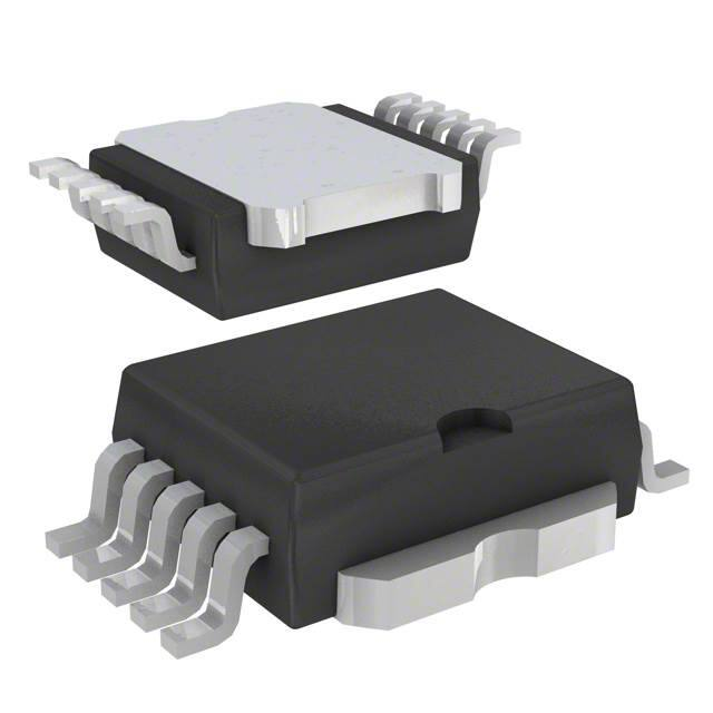


 工商网监
湘ICP备2023018690号
工商网监
湘ICP备2023018690号
