VN31SP
®
HIGH SIDE SMART POWER SOLID STATE RELAY
TYPE
V DSS
R DS(on)
I n(*)
V CC
VN31SP
60 V
0.03 Ω
11.5 A
26 V
■
■
■
■
■
■
■
MAXIMUM CONTINUOUS OUTPUT
CURRENT (#):31 A @ Tc=85oC
5 V LOGIC LEVEL COMPATIBLE INPUT
THERMAL SHUT-DOWN
UNDER VOLTAGE PROTECTION
OPEN DRAIN DIAGNOSTIC OUTPUT
INDUCTIVE LOAD FAST
DEMAGNETIZATION
VERY LOW STAND-BY POWER
DISSIPATION
DESCRIPTION
The VN31SP is a monolithic device made using
STMicroelectronics
VIPower
Technology,
intended for driving resistive or inductive loads
with one side grounded.
Built-in thermal shut-down protects the chip from
over temperature and short circuit.
The open drain diagnostic output indicates: open
load in off state, and in on state, output shorted to
BLOCK DIAGRAM
10
1
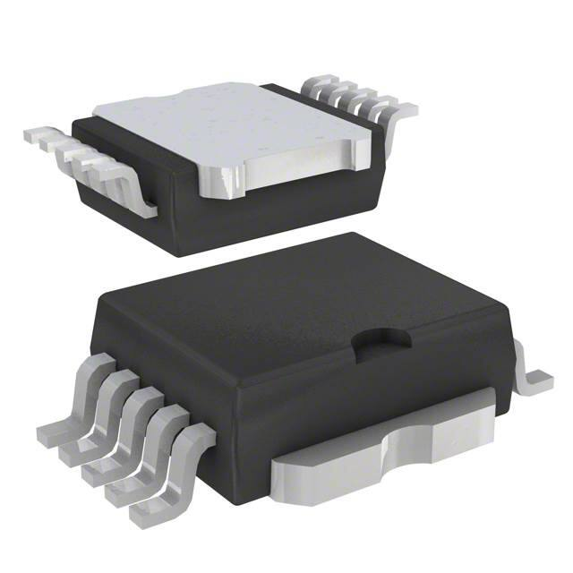
PowerSO-10
VCC and overtemperature. Fast demagnetization
of inductive loads is archivied by negative (-18V)
load voltage at turn-off.
(*) In = Nominal current according to ISO definition for high side automotive switch (see note 1)
(#) The maximum continuous output current is the the current at Tc = 85 oC for a battery voltage of 13V which does not activate self
protection.
September 2013
1/9
�VN31SP
ABSOLUTE MAXIMUM RATING
Symbol
V (BR)DSS
I OUT
Parameter
Value
Unit
Drain-Source Breakdown Voltage
60
V
Output Current (cont.) at T c = 85 o C
31
A
o
IR
Reverse Output Current at T c = 85 C
-31
A
I IN
Input Current
±10
mA
-V CC
Reverse Supply Voltage
I STAT
Status Current
V ESD
Electrostatic Discharge (1.5 kΩ, 100 pF)
P tot
Tj
T stg
o
Power Dissipation at T c = 85 C
V
mA
2000
V
54
W
Junction Operating Temperature
-40 to 150
o
Storage Temperature
-55 to 150
o
CONNECTION DIAGRAMS
CURRENT AND VOLTAGE CONVENTIONS
2/9
-4
±10
C
C
�VN31SP
THERMAL DATA
R thj-case
R thj-amb
Thermal Resistance Junction-case
Thermal Resistance Junction-ambient ($)
Max
Max
o
1.2
50
o
C/W
C/W
($) When mounted using minimum recommended pad size on FR-4 board
ELECTRICAL CHARACTERISTICS (VCC = 13 V; -40 ≤ Tj ≤ 125 oC unless otherwise specified)
POWER
Symbol
VCC
Parameter
Test Conditions
Supply Voltage
o
V DS(on) ≤ 0.5 (note 1)
In(*)
Nominal Current
T c = 85 C
R on
On State Resistance
I OUT = 11.5 A
I OUT = 11.5 A
Supply Current
Off State
On State
IS
V DS(MAX)
Min.
Typ.
Max.
Unit
5.5
13
26
V
11.5
A
T j = 25 o C
T j ≥ 25 o C
Maximum Voltage Drop I OUT = 25 A
T c = 85 o C
0.06
0.03
Ω
Ω
50
15
µA
mA
1.5
V
Max.
Unit
SWITCHING
Symbol
Parameter
t d(on) (^)
Turn-on Delay Time Of
Output Current
I OUT = 11.5 A Resistive Load
Input Rise Time < 0.1 µs
90
µs
Rise Time Of Output
Current
I OUT = 11.5A Resistive Load
Input Rise Time < 0.1 µs
100
µs
Turn-off Delay Time Of
Output Current
I OUT = 11.5 A Resistive Load
Input Rise Time < 0.1 µs
140
µs
Fall Time Of Output
Current
I OUT = 11.5 A Resistive Load
Input Rise Time < 0.1 µs
50
µs
(di/dt) on
Turn-on Current Slope
I OUT = 11.5 A
I OUT = IOV
0.08
0.5
1
A/µs
A/µs
(di/dt) off
Turn-off Current Slope
I OUT = 11.5 A
I OUT = IOV
0.2
3
3
A/µs
A/µs
V demag
Inductive Load Clamp
Voltage
I OUT = 11.5 A
-24
-18
-14
V
Min.
Typ.
Max.
Unit
0.8
V
(•)
V
t r (^)
t d(off) (^)
tf (^)
Test Conditions
L = 1 mH
Min.
Typ.
LOGIC INPUT
Symbol
Parameter
V IL
Input Low Level
Voltage
VIH
Input High Level
Voltage
V I(hyst.)
Input Hysteresis
Voltage
I IN
V ICL
Test Conditions
2
0.5
Input Current
V IN = 5 V
V IN = 2 V
V IN = 0.8 V
Input Clamp Voltage
I IN = 10 mA
I IN = -10 mA
250
V
500
250
25
5.5
6
-0.7
-0.3
µA
µA
µA
V
V
3/9
�VN31SP
ELECTRICAL CHARACTERISTICS (continued)
PROTECTION AND DIAGNOSTICS
Symbol
Parameter
Test Conditions
V STAT
Status Voltage Output
Low
V USD
Under Voltage Shut
Down
V SCL
Status Clamp Voltage
I STAT = 10 mA
I STAT = -10 mA
Over Current
R LOAD < 10 mΩ
I OV
Min.
Typ.
I STAT = 1.6 mA
R LOAD < 10 mΩ
-40 T c 125 o C
o
T c = 85 C
Max.
Unit
0.4
V
5
V
6
-0.7
V
V
140
A
2.5
A
I AV
Average Current in
Short Circuit
I OL
Open Load Current
Level
5
T TSD
Thermal Shut-down
Temperature
140
o
C
TR
Reset Temperature
125
o
C
V OL
Open Load Voltage
Level
Off-State (note 2)
t 1(on)
Open Load Filtering
Time
t 1(off)
600
1250
mA
2.5
3.75
5
V
(note 3)
1
5
10
ms
Open Load Filtering
Time
(note 3)
1
5
10
ms
t 2(off)
Open Load Filtering
Time
(note 3)
1
5
10
ms
t povl
Status Delay
(note 3)
5
10
µs
t pol
Status Delay
(note 3)
50
700
µs
(^) See Switchig Time Waveforms
() The VIH is internally clamped at 6V about. It is possible to connect this pin to an higher voltage via an external resistor calculated to not
exceed 10 mA at the input pin.
note 1: The Nominal Current is the current at Tc = 85 oC for battery voltage of 13V which produces a voltage drop of 0.5 V
note 2: IOL(off) = (VCC -VOL)/ROL (see figure)
note 3: t1(on): minimum open load duration which acctivates the status output
t1(off): minimum load recovery time which desactivates the status output
t2(off): minimum on time after thermal shut down which desactivates status output
tpovl tpol: ISO definition (see figure)
Note 2 Relevant Figure
4/9
Note 3 Relevant Figure
�VN31SP
Switching Time Waveforms
FUNCTIONAL DESCRIPTION
The device has a diagnostic output which
indicates open load conditions in off state as well
as in on state, output shorted to VCC and
overtemperature. The truth table shows input,
diagnostic and output voltage level in normal
operation and in fault conditions. The output
signals are processed by internal logic. The
open load diagnostic output has a 5 ms filtering.
The filter gives a continuous signal for the fault
condition after an initial delay of about 5 ms. This
means that a disconnection during normal
operation, with a duration of less than 5 ms does
not affect the status output. Equally, any
re-connection of less than 5 ms during a
disconnection duration does not affect the status
output. No delay occur for the status to go low in
case of overtemperature conditions. From the
falling edge of the input signal the status output
initially low in fault condition (over temperature or
open load) will go back with a delay (tpovl)in case
of overtemperature condition and a delay (tpol) in
case of open load. These feature fully comply
with International Standard Office (I.S.O.)
requirement for automotive High Side Driver.
To protect the device against short circuit and
over current conditions, the thermal protection
turns the integrated Power MOS off
at
a
minimum
junction
temperature of 140 oC.
When the temperature returns to 125 oC the
switch is automatically turned on again. In short
circuit the protection reacts with virtually no
delay, the sensor being located in the region of
the die where the heat is generated. Driving
inductive loads, an internal function of the
device ensures the fast demagnetization with a
typical voltage (Vdemag) of -18V.
This function allows to greatly reduce the power
dissipation according to the formula:
Pdem = 0.5 • Lload • (Iload)2• [(VCC+Vdemag)/Vdemag]
•f
where f = switching frequency and
Vdemag = demagnetization voltage
Based on this formula it is possible to know
the value of inductance and/or current to avoid
a thermal shut-down. The maximum inductance
which causes the chip temperature to reach the
shut down temperature in a specific thermal
environment, is infact a function of the load
current for a fixed VCC, Vdemag and f.
PROTECTING THE DEVICE AGAIST LOAD
DUMP - TEST PULSE 5
The device is able to withstand the test pulse
No. 5 at level II (Vs = 46.5V) according to the
ISO T/R 7637/1
without
any
external
component. This means that all functions of the
device are performed as designed
after
exposure to disturbance at level II. The VN06SP
is able to withstand the test pulse No.5 at level
III adding an external resistor of 150 ohm
between GND pin and ground plus a filter
capacitor of 1000 µF between VCC pin and
ground (if RLOAD ≤ 20 Ω).
PROTECTING
THE
DEVICE
AGAINST
REVERSE BATTERY
The simplest way to protect the device against a
continuous reverse battery voltage (-26V) is to
insert a Schottky diode between GND pin and
ground, as shown in the typical application circuit
(fig.3).
The consequences of the voltage drop across
this diode are as follows:
If the input is pulled to power GND, a negative
voltage of -Vf is seen by the device. (Vil, Vih
thresholds and Vstat are increased by Vf with
respect to power GND).
The undervoltage shutdown level is increa- sed
by Vf.
If there is no need for the control unit to handle
external analog signals referred to the power
GND, the best approach is to connect the
reference potential of the control unit to node [6]
(see application circuit in fig. 4), which becomes
the common signal GND for the whole control
board avoiding shift of Vih, Vil and Vstat. This
solution allows the use of a standard diode.
5/9
�VN31SP
TRUTH TABLE
INPUT
OUTPUT
DIAGNOSTIC
Normal Operation
L
H
L
H
H
H
Open Circuit (No Load)
H
H
L
Over-temperature
H
L
L
Under-voltage
X
L
H
Short load to V CC
L
H
L
Figure 1: Waveforms
Figure 2: Over Current Test Circuit
6/9
�VN31SP
Figure 3: Typical Application Circuit With A Schottky Diode For Reverse Supply Protection
Figure 4: Typical Application Circuit With Separate Signal Ground
7/9
�VN31SP
PowerSO-10 MECHANICAL DATA
mm
DIM.
MIN.
inch
TYP.
MAX.
MIN.
TYP.
MAX.
A
3.35
3.65
0.132
0.144
A1
0.00
0.10
0.000
0.004
B
0.40
0.60
0.016
0.024
c
0.35
0.55
0.013
0.022
D
9.40
9.60
0.370
0.378
D1
7.40
7.60
0.291
0.300
E
9.30
9.50
0.366
0.374
E1
7.20
7.40
0.283
0.291
E2
7.20
7.60
0.283
0.300
E3
6.10
6.35
0.240
0.250
E4
5.90
6.10
0.232
e
1.27
0.240
0.050
F
1.25
1.35
0.049
0.053
H
13.80
14.40
0.543
0.567
1.80
0.047
h
0.50
L
0.002
1.20
q
1.70
α
0.071
0.067
0o
8o
B
0.10 A B
10
=
E4
=
=
=
E1
=
E3
=
E2
=
E
=
=
=
H
6
=
=
1
5
B
e
0.25
SEATING
PLANE
DETAIL "A"
A
C
M
Q
D
h
= D1 =
=
=
SEATING
PLANE
A
F
A1
A1
L
DETAIL "A"
α
0068039-C
8/9
�VN31SP
Please Read Carefully:
Information in this document is provided solely in connection with ST products. STMicroelectronics NV and its subsidiaries (“ST”) reserve the
right to make changes, corrections, modifications or improvements, to this document, and the products and services described herein at any
time, without notice.
All ST products are sold pursuant to ST’s terms and conditions of sale.
Purchasers are solely responsible for the choice, selection and use of the ST products and services described herein, and ST assumes no
liability whatsoever relating to the choice, selection or use of the ST products and services described herein.
No license, express or implied, by estoppel or otherwise, to any intellectual property rights is granted under this document. If any part of this
document refers to any third party products or services it shall not be deemed a license grant by ST for the use of such third party products
or services, or any intellectual property contained therein or considered as a warranty covering the use in any manner whatsoever of such
third party products or services or any intellectual property contained therein.
UNLESS OTHERWISE SET FORTH IN ST’S TERMS AND CONDITIONS OF SALE ST DISCLAIMS ANY EXPRESS OR IMPLIED
WARRANTY WITH RESPECT TO THE USE AND/OR SALE OF ST PRODUCTS INCLUDING WITHOUT LIMITATION IMPLIED
WARRANTIES OF MERCHANTABILITY, FITNESS FOR A PARTICULAR PURPOSE (AND THEIR EQUIVALENTS UNDER THE LAWS
OF ANY JURISDICTION), OR INFRINGEMENT OF ANY PATENT, COPYRIGHT OR OTHER INTELLECTUAL PROPERTY RIGHT.
ST PRODUCTS ARE NOT DESIGNED OR AUTHORIZED FOR USE IN: (A) SAFETY CRITICAL APPLICATIONS SUCH AS LIFE
SUPPORTING, ACTIVE IMPLANTED DEVICES OR SYSTEMS WITH PRODUCT FUNCTIONAL SAFETY REQUIREMENTS; (B)
AERONAUTIC APPLICATIONS; (C) AUTOMOTIVE APPLICATIONS OR ENVIRONMENTS, AND/OR (D) AEROSPACE APPLICATIONS
OR ENVIRONMENTS. WHERE ST PRODUCTS ARE NOT DESIGNED FOR SUCH USE, THE PURCHASER SHALL USE PRODUCTS AT
PURCHASER’S SOLE RISK, EVEN IF ST HAS BEEN INFORMED IN WRITING OF SUCH USAGE, UNLESS A PRODUCT IS
EXPRESSLY DESIGNATED BY ST AS BEING INTENDED FOR “AUTOMOTIVE, AUTOMOTIVE SAFETY OR MEDICAL” INDUSTRY
DOMAINS ACCORDING TO ST PRODUCT DESIGN SPECIFICATIONS. PRODUCTS FORMALLY ESCC, QML OR JAN QUALIFIED ARE
DEEMED SUITABLE FOR USE IN AEROSPACE BY THE CORRESPONDING GOVERNMENTAL AGENCY.
Resale of ST products with provisions different from the statements and/or technical features set forth in this document shall immediately void
any warranty granted by ST for the ST product or service described herein and shall not create or extend in any manner whatsoever, any
liability of ST.
ST and the ST logo are trademarks or registered trademarks of ST in various countries.
Information in this document supersedes and replaces all information previously supplied.
The ST logo is a registered trademark of STMicroelectronics. All other names are the property of their respective owners.
© 2013 STMicroelectronics - All rights reserved
STMicroelectronics group of companies
Australia - Belgium - Brazil - Canada - China - Czech Republic - Finland - France - Germany - Hong Kong - India - Israel - Italy - Japan Malaysia - Malta - Morocco - Philippines - Singapore - Spain - Sweden - Switzerland - United Kingdom - United States of America
www.st.com
DocID1099 Rev 2
9/9
9
�
很抱歉,暂时无法提供与“VN31SP13TR”相匹配的价格&库存,您可以联系我们找货
免费人工找货