VN340SP-E & VN340SP-33-E
Datasheet
Quad high-side smart power solid-state relay
Features
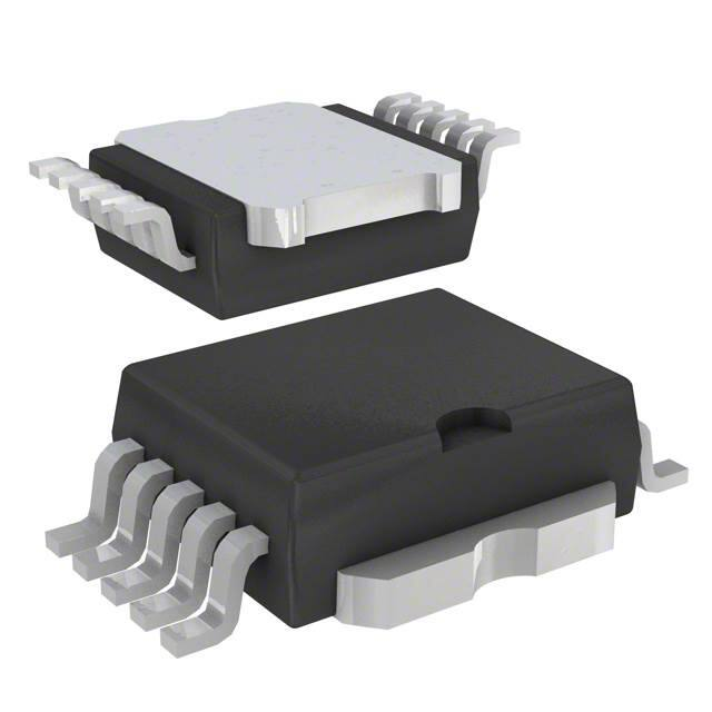
PowerSO-10
Product status link
VN340SP-E & VN340SP-33-E
Product label
•
•
•
•
•
•
•
•
•
Operating output current: 0.7 A (VN340SP-E) or 1 A (VN340SP-33-E)
Digital I/O clamped at 32 V minimum voltage
Shorted load and overtemperature protections
Protection against loss of ground
Built-in current limiter
Undervoltage shutdown
Open drain diagnostic output
Fast demagnetization of inductive loads
Conforms to IEC 61131-2
Applications
•
•
•
•
Vending machines
Industrial PC peripheral input/output
Numerical control machines
General high-side switch applications
Description
VN340SP-E & VN340SP-33-E are monolithic devices developed using
STMicroelectronics' VIPower technology, intended to drive four independent resistive
or inductive loads with one side connected to ground. Active current limitation
prevents dropping of the system power supply in case of shorted load. Built-in
thermal shutdown protects the chip from overtemperature and short-circuit. The open
drain diagnostic output indicates overtemperature conditions. Each I/O is pulled down
when the overtemperature condition of the relative channel is verified.
DS4346 - Rev 5 - September 2022
For further information contact your local STMicroelectronics sales office.
www.st.com
�VN340SP-E & VN340SP-33-E
Block diagram
1
Block diagram
Figure 1. Block diagram
DS4346 - Rev 5
page 2/20
�VN340SP-E & VN340SP-33-E
Pin connection
2
Pin connection
Figure 2. Connection diagram (top view)
Figure 3. Current and voltage conventions
VCC
IIN1
VIN1
10
VIN2
VIN3
VIN4
IIN2
IIN3
IIN4
IDIAG
VDIAG
DS4346 - Rev 5
9 I/O2
I/O1
11
VCC
OUT1
1
8 I/O3
OUT2
2
7 I/O4
OUT3
3
OUT4
4
6 DIAG
GND
5
IOUT1
IOUT2
IOUT3
IOUT4
VOUT1
VOUT2
VOUT3
VOUT4
page 3/20
�VN340SP-E & VN340SP-33-E
Maximum ratings
3
Maximum ratings
Table 1. Absolute maximum ratings
Symbol
Parameter
Value
Unit
VCC
Power supply voltage
45
V
-VCC
Reverse supply voltage
-4
V
IOUT
Output current
Internally limited
A
-6
A
IR
Reverse output current (per channel)
IIN
Input current range
-1 to +10
mA
IDIAG
Diag pin current
-1 to +10
mA
VESD
Electrostatic discharge (R = 1.5 kΩ; C = 100 pF)
2000
V
Single pulse avalanche energy, one channel active, TJ = 125 °C, ILOAD = 0.625 A
10
J
EAS
Single pulse avalanche energy all channels active simultaneously, TJ = 125 °C, ILOAD =
0.625 A
2
J
PTOT
Power dissipation at TC = 25 °C
Internally limited
W
TJ
Junction operating temperature
Internally limited
°C
-55 to 150
°C
TSTG
Storage temperature
Table 2. Thermal data
Symbol
Rth(JC)
Rth(JA)
Parameter
Thermal resistance junction-case
(1)
Thermal resistance junction-ambient (2)
Max Value
Unit
3
°C/W
50
°C/W
1. Per channel.
2. When mounted on a four-layer FR4, with the minimum recommended pad size.
DS4346 - Rev 5
page 4/20
�VN340SP-E & VN340SP-33-E
Electrical characteristics
4
Electrical characteristics
10 V < VCC < 36 V; -40 °C < TJ < 125 °C; unless otherwise specified
Table 3. Power section
Symbol
Parameter
VCC
Supply voltage
RDS(on)
Test conditions
Min.
Typ.
10
On-state resistance
Max.
Unit
36
V
IOUT = 0.5 A @ TJ = 25 °C
0.2
IOUT = 0.5 A @ TJ = 85 °C
0.32
IOUT = 0.5 A @ TJ = 125 °C
0.4
All channels in OFF-state
1
VIN = 30 V, IOUT = 0 V, TJ = 125 °C
6
Ω
IS
Supply current
VOL
Low state output voltage
VIN = VIL; RLOAD > = 10 MΩ
1.5
V
ILGND
Output current at turn-off
VCC = VIN = VGND = VSTAT = 18 to 30
V, TA = - 25 °C to 85 °C
2
mA
Vdemag
Demagnetization voltage
IOUT = 0.5 A; LLOAD >= 1 mH
VCC-55
VCC-45
V
Typ.
Max.
Unit
52
100
94
250
34
50
8
20
Typ.
Max.
Unit
2
V
VCC-65
mA
Table 4. Switching (VCC = 24 V, TJ = 25 °C)
Symbol
Parameter
td(ON)
Turn-on delay time
tr
Rise time of output current
td(OFF)
Turn-off delay time of output
current
tf
Fall time
Test conditions
Min.
IOUT = 0.5 A, resistive load, input rise
time < 0.1 µs
µs
Table 5. Logic inputs
Symbol
Parameter
VIL
I/O input low level voltage
VIH
I/O input high level voltage
VI(HYST)
I/O input hysteresis voltage
IIN
I/O input current
VICL
I/O input clamp voltage(1)
Test conditions
Min.
3.5
V
0.5
VIN = 30 V
IIN = 1 mA
IIN = -1 mA
V
25
32
36
-0.7
µA
V
1. The input voltage is internally clamped at 32 V minimum, the input pins can be connected to a higher voltage by an external
resistor, which cannot exceed 10 mA
DS4346 - Rev 5
page 5/20
�VN340SP-E & VN340SP-33-E
Electrical characteristics
Table 6. Protection and diagnostic
Symbol
(1)
VDIAG
Parameter
Test conditions
Status voltage output low
IDIAG = 5 mA (fault condition)
IDIAG = 1 mA
VSCL
Status clamp voltage
VUSD
Undervoltage shutdown
Ilim
DC short-circuit current
VCC = 24 V; RLOAD < 10 mΩ
IOVPK
Peak short-circuit current
IDIAGH
Min.
32
IDIAG = -1 mA
Typ.
Max.
Unit
1
V
36
V
-0.7
V
5
8
V
2
A
VCC = 24 V; VIN = 30 V; RLOAD < 10
mΩ
4
A
Leakage on DIAG pin in high
state
VDIAG = 24 V
25
μA
ILOAD
Output leakage current
VCC = 10 to 36 V; VIN=VIL
50
μA
tSC
Delay time of current limiter
100
μs
TTSD
Junction shutdown
temperature
150
170
°C
TR
Junction reset temperature
135
155
°C
0.7(2)
1(3)
1. Status determination > 100 μs after the switching edge.
2. VN340SP-E
3. VN340SP-33-E
Note:
DS4346 - Rev 5
If the INPUT pin is left floating the corresponding channel automatically switches off. If GND pin is disconnected
the channel switches off provided that VCC does not exceed 36 V.
page 6/20
�VN340SP-E & VN340SP-33-E
Test circuits
5
Test circuits
Figure 4. Avalanche energy test circuit
+VCC
10 k Ω
I/On
CONTROL
UNIT
DIAG
OUTPUT
RIN
LOAD
GND
GND
Figure 5. Peak short-circuit test diagram
+VCC
10kΩ
I/On
CONTROL
UNIT
DIAG
OUTPUT
RIN
RL < 10 m Ω
GND
GND
DS4346 - Rev 5
page 7/20
�VN340SP-E & VN340SP-33-E
Test circuits
Figure 6. ILGND test configuration
DS4346 - Rev 5
page 8/20
�VN340SP-E & VN340SP-33-E
Switching time waveforms and truth table
6
Switching time waveforms and truth table
Figure 7. Switching waveforms
Figure 8. Switching parameter test conditions
DS4346 - Rev 5
page 9/20
�VN340SP-E & VN340SP-33-E
Switching time waveforms and truth table
Table 7. Truth table
Conditions
MCOUTn
I/On
OUTPUTn
Diagnostic
L
L
L
H
H
H
H
H
L
L
L
H
H
L
L
L
L
L
L
H(1)
H
H
L
H(1)
L
L
L
H
H
H(2)
H
Normal operation
Junction overtemperature
Undervoltage
Shorted load (current limitation)
H
1. DIAG pin is considered pulled-up at application voltage level
2. VOUT = RLOAD x ILIM
Figure 9. Driving circuit
Notes:
DS4346 - Rev 5
•
The I/OS are internally pulled-down
•
REXT is for enhancement of EMI robustness
page 10/20
�VN340SP-E & VN340SP-33-E
Package information
7
Package information
In order to meet environmental requirements, ST offers these devices in different grades of ECOPACK packages,
depending on their level of environmental compliance. ECOPACK specifications, grade definitions and product
status are available at: www.st.com. ECOPACK is an ST trademark.
7.1
PowerSO-10 package information
Figure 10. PowerSO-10 package outline
DS4346 - Rev 5
page 11/20
�VN340SP-E & VN340SP-33-E
PowerSO-10 package information
Table 8. PowerSO-10 package mechanical data
Dim.
mm
Min.
Typ.
Max.
A1
0
0.05
0.08
A2
3.45
3.5
3.55
A3
1.24
1.28
1.32
A4
0.15
0.2
0.25
a
0.2
b
0.4
0.45
0.5
c
0.24
0.27
0.3
D
9.45
9.52
9.59
D1
7.42
7.5
7.58
d
0
0.04
0.09
E
13.9
14.1
14.3
E1(1)
9.33
9.4
9.47
E2
7.4
7.42
7.5
E3
5.95
6.1
6.25
e
1.22
1.27
1.32
e1
5.08
F
0.5
G
1.2
L
0.85
1
R1
0.25
R2
T
1.1
0.8
3 deg
5 deg
T1
6 deg
T2
10 deg
7 deg
1. Resin protrusions are not included (max. value 0.15 mm per side)
DS4346 - Rev 5
page 12/20
�VN340SP-E & VN340SP-33-E
PowerSO-10 packing information
7.2
PowerSO-10 packing information
Figure 11. PowerSO-10 career tape outline
Note:
Drawing is not in scale
Table 9. PowerSO-10 career tape dimension mechanical data
Dim.
Note:
DS4346 - Rev 5
mm
Min.
Typ.
Max.
A0
14.9
15.0
15.1
B0
9.9
10.0
10.1
K0
4.15
4.25
4.35
F
11.4
11.5
11.6
E
1.65
1.75
1.85
W
23.7
24.0
24.3
P2
1.9
2.0
2.1
P0
3.9
4.0
4.1
P1
23.9
24.0
24.1
T
0.025
0.30
0.35
D(Ø)
1.50
1.55
1.60
10 sprocket hole pitch cumulative tolerance ±0.2 mm
page 13/20
�VN340SP-E & VN340SP-33-E
PowerSO-10 packing information
Figure 12. PowerSO-10 reel outline
Note:
Drawing is not in scale
Table 10. PowerSO-10 reel dimension mechanical data
mm
Dim.
Min.
Typ.
Max.
A
330
B
1.5
C
12.8
D
20.2
N
60
G
23.7
13
13.2
24.4
T
Note:
30.4
10 sprocket hole pitch cumulative tolerance ±0.2 mm
Table 11. PowerSO-10 base and bulk quantity
DS4346 - Rev 5
Base quantity
Bulk quantity
600
600
page 14/20
�VN340SP-E & VN340SP-33-E
Ordering information
8
Ordering information
Table 12. Ordering information
Part Number
Package
VN340SP-E
VN340SPTR-E
VN340SP-33-E
VN340SPTR-33-E
DS4346 - Rev 5
Packaging
Tube
PowerSO-10
Tape and reel
Tube
Tape and reel
page 15/20
�VN340SP-E & VN340SP-33-E
Revision history
Table 13. Document revision history
DS4346 - Rev 5
Date
Revision
Changes
05-Sep-2005
1
Initial release.
19-Mar-2007
2
Document reformatted, typo in note 1.
22-Aug-2008
3
Updated table 9.
07-Sep-2015
4
Updated the table of absolute maximum ratings.
1-Sep-2022
5
Merged VN340SP-33 and VN340SP DS; some minor changes
page 16/20
�VN340SP-E & VN340SP-33-E
Contents
Contents
1
Block diagram . . . . . . . . . . . . . . . . . . . . . . . . . . . . . . . . . . . . . . . . . . . . . . . . . . . . . . . . . . . . . . . . . . . . .2
2
Pin connection . . . . . . . . . . . . . . . . . . . . . . . . . . . . . . . . . . . . . . . . . . . . . . . . . . . . . . . . . . . . . . . . . . . .3
3
Maximum ratings . . . . . . . . . . . . . . . . . . . . . . . . . . . . . . . . . . . . . . . . . . . . . . . . . . . . . . . . . . . . . . . . . .4
4
Electrical characteristics. . . . . . . . . . . . . . . . . . . . . . . . . . . . . . . . . . . . . . . . . . . . . . . . . . . . . . . . . . . 5
5
Test circuits . . . . . . . . . . . . . . . . . . . . . . . . . . . . . . . . . . . . . . . . . . . . . . . . . . . . . . . . . . . . . . . . . . . . . . .7
6
Switching time waveforms and truth table. . . . . . . . . . . . . . . . . . . . . . . . . . . . . . . . . . . . . . . . . . 9
7
Package information. . . . . . . . . . . . . . . . . . . . . . . . . . . . . . . . . . . . . . . . . . . . . . . . . . . . . . . . . . . . . .11
8
7.1
PowerSO-10 package information . . . . . . . . . . . . . . . . . . . . . . . . . . . . . . . . . . . . . . . . . . . . . . . 11
7.2
PowerSO-10 packing information . . . . . . . . . . . . . . . . . . . . . . . . . . . . . . . . . . . . . . . . . . . . . . . . 13
Ordering information . . . . . . . . . . . . . . . . . . . . . . . . . . . . . . . . . . . . . . . . . . . . . . . . . . . . . . . . . . . . .15
Revision history . . . . . . . . . . . . . . . . . . . . . . . . . . . . . . . . . . . . . . . . . . . . . . . . . . . . . . . . . . . . . . . . . . . . . . .16
List of tables . . . . . . . . . . . . . . . . . . . . . . . . . . . . . . . . . . . . . . . . . . . . . . . . . . . . . . . . . . . . . . . . . . . . . . . . . .18
List of figures. . . . . . . . . . . . . . . . . . . . . . . . . . . . . . . . . . . . . . . . . . . . . . . . . . . . . . . . . . . . . . . . . . . . . . . . . .19
DS4346 - Rev 5
page 17/20
�VN340SP-E & VN340SP-33-E
List of tables
List of tables
Table 1.
Table 2.
Table 3.
Table 4.
Table 5.
Table 6.
Table 7.
Table 8.
Table 9.
Table 10.
Table 11.
Table 12.
Table 13.
Absolute maximum ratings . . . . . . . . . . . . . . . . . . .
Thermal data. . . . . . . . . . . . . . . . . . . . . . . . . . . . .
Power section . . . . . . . . . . . . . . . . . . . . . . . . . . . .
Switching (VCC = 24 V, TJ = 25 °C). . . . . . . . . . . . . .
Logic inputs. . . . . . . . . . . . . . . . . . . . . . . . . . . . . .
Protection and diagnostic . . . . . . . . . . . . . . . . . . . .
Truth table . . . . . . . . . . . . . . . . . . . . . . . . . . . . . .
PowerSO-10 package mechanical data . . . . . . . . . .
PowerSO-10 career tape dimension mechanical data .
PowerSO-10 reel dimension mechanical data . . . . . .
PowerSO-10 base and bulk quantity. . . . . . . . . . . . .
Ordering information. . . . . . . . . . . . . . . . . . . . . . . .
Document revision history . . . . . . . . . . . . . . . . . . . .
DS4346 - Rev 5
.
.
.
.
.
.
.
.
.
.
.
.
.
.
.
.
.
.
.
.
.
.
.
.
.
.
.
.
.
.
.
.
.
.
.
.
.
.
.
.
.
.
.
.
.
.
.
.
.
.
.
.
.
.
.
.
.
.
.
.
.
.
.
.
.
.
.
.
.
.
.
.
.
.
.
.
.
.
.
.
.
.
.
.
.
.
.
.
.
.
.
.
.
.
.
.
.
.
.
.
.
.
.
.
.
.
.
.
.
.
.
.
.
.
.
.
.
.
.
.
.
.
.
.
.
.
.
.
.
.
.
.
.
.
.
.
.
.
.
.
.
.
.
.
.
.
.
.
.
.
.
.
.
.
.
.
.
.
.
.
.
.
.
.
.
.
.
.
.
.
.
.
.
.
.
.
.
.
.
.
.
.
.
.
.
.
.
.
.
.
.
.
.
.
.
.
.
.
.
.
.
.
.
.
.
.
.
.
.
.
.
.
.
.
.
.
.
.
.
.
.
.
.
.
.
.
.
.
.
.
.
.
.
.
.
.
.
.
.
.
.
.
.
.
.
.
.
.
.
.
.
.
.
.
.
.
.
.
.
.
.
.
.
.
.
.
.
.
.
.
.
.
.
.
.
.
.
.
.
.
.
.
.
.
.
.
.
.
.
.
.
.
.
.
.
.
.
.
.
.
.
.
.
.
.
.
.
.
.
.
.
.
.
.
.
.
.
.
.
.
.
.
.
.
.
.
.
.
.
.
.
.
.
.
.
.
.
.
.
.
.
.
.
.
.
.
.
.
.
.
.
.
.
.
.
.
.
.
.
.
.
.
.
.
.
.
.
.
.
.
.
.
.
.
.
.
.
.
.
.
.
.
.
.
.
.
.
.
.
.
.
.
.
.
.
.
.
.
.
.
.
.
.
.
.
.
.
.
.
.
.
.
.
.
.
.
.
.
.
.
.
.
.
.
.
.
.
.
.
.
.
.
.
.
.
.
.
.
.
.
.
.
.
.
.
.
.
.
.
.
.
.
.
.
.
.
.
.
.
.
.
.
.
.
.
.
.
.
.
.
.
.
.
.
.
.
.
.
.
.
.
.
.
.
.
.
.
.
.
.
.
.
.
.
.
.
.
.
.
.
.
.
.
.
.
.
.
.
.
.
.
.
.
.
.
.
.
.
.
.
.
.
.
.
.
.
.
.
.
.
.
.
.
. 4
. 4
. 5
. 5
. 5
. 6
10
12
13
14
14
15
16
page 18/20
�VN340SP-E & VN340SP-33-E
List of figures
List of figures
Figure 1.
Figure 2.
Figure 3.
Figure 4.
Figure 5.
Figure 6.
Figure 7.
Figure 8.
Figure 9.
Figure 10.
Figure 11.
Figure 12.
DS4346 - Rev 5
Block diagram . . . . . . . . . . . . . . .
Connection diagram (top view) . . . .
Current and voltage conventions. . .
Avalanche energy test circuit . . . . .
Peak short-circuit test diagram . . . .
ILGND test configuration . . . . . . . . .
Switching waveforms. . . . . . . . . . .
Switching parameter test conditions
Driving circuit . . . . . . . . . . . . . . . .
PowerSO-10 package outline . . . . .
PowerSO-10 career tape outline . . .
PowerSO-10 reel outline . . . . . . . .
.
.
.
.
.
.
.
.
.
.
.
.
.
.
.
.
.
.
.
.
.
.
.
.
.
.
.
.
.
.
.
.
.
.
.
.
.
.
.
.
.
.
.
.
.
.
.
.
.
.
.
.
.
.
.
.
.
.
.
.
.
.
.
.
.
.
.
.
.
.
.
.
.
.
.
.
.
.
.
.
.
.
.
.
.
.
.
.
.
.
.
.
.
.
.
.
.
.
.
.
.
.
.
.
.
.
.
.
.
.
.
.
.
.
.
.
.
.
.
.
.
.
.
.
.
.
.
.
.
.
.
.
.
.
.
.
.
.
.
.
.
.
.
.
.
.
.
.
.
.
.
.
.
.
.
.
.
.
.
.
.
.
.
.
.
.
.
.
.
.
.
.
.
.
.
.
.
.
.
.
.
.
.
.
.
.
.
.
.
.
.
.
.
.
.
.
.
.
.
.
.
.
.
.
.
.
.
.
.
.
.
.
.
.
.
.
.
.
.
.
.
.
.
.
.
.
.
.
.
.
.
.
.
.
.
.
.
.
.
.
.
.
.
.
.
.
.
.
.
.
.
.
.
.
.
.
.
.
.
.
.
.
.
.
.
.
.
.
.
.
.
.
.
.
.
.
.
.
.
.
.
.
.
.
.
.
.
.
.
.
.
.
.
.
.
.
.
.
.
.
.
.
.
.
.
.
.
.
.
.
.
.
.
.
.
.
.
.
.
.
.
.
.
.
.
.
.
.
.
.
.
.
.
.
.
.
.
.
.
.
.
.
.
.
.
.
.
.
.
.
.
.
.
.
.
.
.
.
.
.
.
.
.
.
.
.
.
.
.
.
.
.
.
.
.
.
.
.
.
.
.
.
.
.
.
.
.
.
.
.
.
.
.
.
.
.
.
.
.
.
.
.
.
.
.
.
.
.
.
.
.
.
.
.
.
.
.
.
.
.
.
.
.
.
.
.
.
.
.
.
.
.
.
.
.
.
.
.
.
.
.
.
.
.
.
.
.
.
.
.
.
.
.
.
.
.
.
.
.
.
.
.
.
.
.
.
.
.
.
.
.
.
.
.
.
.
.
.
.
.
.
.
.
.
.
.
.
.
.
.
.
.
.
.
.
.
.
.
.
.
.
.
.
.
.
.
.
.
.
.
.
.
.
.
.
.
.
.
.
.
.
.
.
.
.
.
.
.
.
.
.
.
.
.
.
.
.
.
.
.
.
.
.
.
.
.
.
.
.
.
.
.
.
.
.
.
.
.
.
.
.
.
.
.
.
.
.
.
.
.
.
.
.
.
.
.
.
.
.
.
.
.
.
.
.
.
.
.
.
.
.
.
.
.
.
.
.
.
.
.
.
.
.
.
.
.
.
.
.
.
.
.
.
.
.
.
.
.
.
.
.
.
.
.
. 2
. 3
. 3
. 7
. 7
. 8
. 9
. 9
10
11
13
14
page 19/20
�VN340SP-E & VN340SP-33-E
IMPORTANT NOTICE – READ CAREFULLY
STMicroelectronics NV and its subsidiaries (“ST”) reserve the right to make changes, corrections, enhancements, modifications, and improvements to ST
products and/or to this document at any time without notice. Purchasers should obtain the latest relevant information on ST products before placing orders. ST
products are sold pursuant to ST’s terms and conditions of sale in place at the time of order acknowledgment.
Purchasers are solely responsible for the choice, selection, and use of ST products and ST assumes no liability for application assistance or the design of
purchasers’ products.
No license, express or implied, to any intellectual property right is granted by ST herein.
Resale of ST products with provisions different from the information set forth herein shall void any warranty granted by ST for such product.
ST and the ST logo are trademarks of ST. For additional information about ST trademarks, refer to www.st.com/trademarks. All other product or service names
are the property of their respective owners.
Information in this document supersedes and replaces information previously supplied in any prior versions of this document.
© 2022 STMicroelectronics – All rights reserved
DS4346 - Rev 5
page 20/20
�
很抱歉,暂时无法提供与“VN340SP-33-E”相匹配的价格&库存,您可以联系我们找货
免费人工找货- 国内价格
- 1+134.27410
- 10+111.89510
- 50+89.51600
- 100+74.59670